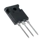
Low VCE(sat) IGBT
High speed IGBT
IXGH/IXGM 20 N60
IXGH/IXGM 20 N60A
Symbol
Test Conditions
Maximum Ratings
VCES
TJ = 25°C to 150°C
600
V
VCGR
TJ = 25°C to 150°C; RGE = 1 MΩ
600
V
VGES
Continuous
±20
V
VGEM
Transient
±30
V
I C25
TC = 25°C
40
A
I C90
TC = 90°C
20
A
I CM
TC = 25°C, 1 ms
80
A
SSOA
(RBSOA)
VGE = 15 V, T VJ = 125°C, RG = 82 Ω
Clamped inductive load, L = 100 µH
ICM = 40
@ 0.8 VCES
A
PC
TC = 25°C
150
W
-55 ... +150
°C
TJM
150
°C
Tstg
-55 ... +150
°C
TJ
Md
Mounting torque (M3)
1.13/10 Nm/lb.in.
Weight
TO-204 = 18 g, TO-247 = 6 g
Maximum lead temperature for soldering
1.6 mm (0.062 in.) from case for 10 s
°C
300
VCES
IC25
VCE(sat)
600 V
600 V
40 A
40 A
2.5 V
3.0 V
TO-247 AD (IXGH)
G
C
E
TO-204 AE (IXGM)
C
G = Gate,
E = Emitter,
C = Collector,
TAB = Collector
Features
International standard packages
2nd generation HDMOSTM process
Low VCE(sat)
- for low on-state conduction losses
High current handling capability
MOS Gate turn-on
- drive simplicity
Voltage rating guaranteed at high
temperature (125°C)
l
l
l
l
l
l
Symbol
Test Conditions
Characteristic Values
(TJ = 25°C, unless otherwise specified)
min. typ. max.
Applications
AC motor speed control
DC servo and robot drives
DC choppers
Uninterruptible power supplies (UPS)
Switch-mode and resonant-mode
power supplies
l
BVCES
IC
= 250 µA, VGE = 0 V
600
VGE(th)
IC
= 250 µA, VCE = VGE
2.5
ICES
VCE = 0.8 • VCES
VGE = 0 V
I GES
VCE = 0 V, VGE = ±20 V
VCE(sat)
IC
= IC90, VGE = 15 V
V
5
V
l
l
l
TJ = 25°C
TJ = 125°C
20N60
20N60A
200
1
µA
mA
±100
nA
2.5
3.0
V
V
l
Advantages
Easy to mount with 1 screw (TO-247)
(isolated mounting screw hole)
High power density
l
l
© 1996 IXYS All rights reserved
91511F (3/96)
�IXGH 20N60
IXGM 20N60
IXGH 20N60A IXGM 20N60A
Symbol
Test Conditions
Characteristic Values
(TJ = 25°C, unless otherwise specified)
min. typ. max.
gfs
I C = IC90; VCE = 10 V,
Pulse test, t ≤ 300 µs, duty cycle ≤ 2 %
6
14
S
1500
pF
200
pF
Cres
40
pF
Qg
100
120
nC
20
30
nC
60
90
nC
Cies
Coes
Qge
VCE = 25 V, VGE = 0 V, f = 1 MHz
IC = IC90, VGE = 15 V, VCE = 0.5 VCES
Qgc
Eoff
Inductive load, T J = 25°°C
IC = IC90 , VGE = 15 V, L = 300 µH
VCE = 0.8 VCES, RG = Roff = 82 Ω
Switching times may increase
for VCE (Clamp) > 0.8 • V CES, 20N60A
higher TJ or increased RG
20N60A
td(on)
Inductive load, TJ = 25°°C
100
ns
tri
IC = IC90, VGE = 15 V,
L = 300 µH
200
ns
2
mJ
td(on)
tri
td(off)
tfi
Eon
td(off)
tfi
Eoff
VCE = 0.8 VCES,
RG = R off = 82 Ω
Remarks: Switching times
may increase for VCE
(Clamp) > 0.8 • V CES,
higher TJ or increased RG
100
ns
200
ns
600
ns
200
ns
1.5
mJ
900
1500
ns
20N60
20N60A
530
250
2000
600
ns
ns
20N60
20N60A
3.2
2.0
RthCK
1 = Gate
2 = Collector
3 = Emitter
Tab = Collector
mJ
mJ
0.83 K/W
RthJC
TO-247 AD Outline
0.25
TO-204AE Outline
K/W
IXGH 20N60 and IXGH 20N60A characteristic curves are located on the
IXGH 20N60U1 and IXGH 20N60AU1 data sheets.
1 = Gate
2 = Emitter
Case = Collector
IXYS reserves the right to change limits, test conditions, and dimensions.
IXYS MOSFETS and IGBTs are covered by one or more of the following U.S. patents:
4,835,592
4,850,072
4,881,106
4,931,844
5,017,508
5,034,796
5,049,961
5,063,307
5,187,117
5,237,481
5,486,715
5,381,025
�
