Preliminary Technical Information
IXGH25N250
IXGT25N250
IXGV25N250S
High Voltage IGBT
For Capacitor Discharge
Applications
VCES = 2500 V
IC25 = 60 A
VCE(sat) ≤ 2.9 V
TO-247 (IXGH)
Symbol
Test Conditions
Maximum Ratings
VCES
TJ = 25°C to 150°C
2500
V
VCGR
TJ = 25°C to 150°C; RGE = 1 MΩ
2500
V
VGES
Continuous
± 20
V
VGEM
Transient
± 30
V
IC25
TC = 25°C
60
A
IC110
TC = 110°C
25
A
ICM
TC = 25°C, VGE = 20 V, 1 ms
200
A
SSOA
(RBSOA)
VGE = 20 V, TJ = 125°C, RG = 20 Ω
Clamped inductive load @ 1250V
ICM = 240
A
PC
TC = 25°C
250
W
-55 ... +150
°C
TJM
150
°C
Tstg
-55 ... +150
°C
TJ
1.6 mm (0.062 in.) from case for 10 s
300
°C
TSOLD
Plastic body for 10 s
260
°C
Md
Mounting torque (TO-247)
1.13/10
Nm/lb-in
6
4
g
g
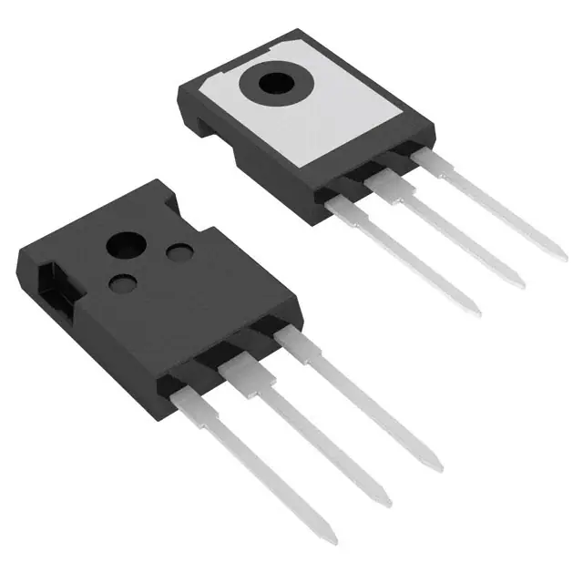
TO-247
TO-268
Symbol
Test Conditions
BVCES
IC
= 250 μA, VGE = 0 V
2500
VGE(th)
IC
= 250 μA, VCE = VGE
3.0
ICES
VCE = 0.8 • VCES
VGE = 0 V
IGES
VCE = 0 V, VGE = ±20 V
VCE(sat)
IC
IC
Characteristic Values
(TJ = 25°C unless otherwise specified)
Min. Typ. Max.
TJ = 125°C
= 25 A, VGE = 15 V
= 75 A
© 2007 IXYS CORPORATION, All rights reserved
C
C (TAB)
E
TO-268 (IXGT)
G
E
C (TAB)
PLUS220SMD (IXGV...S)
TL
Weight
G
G
E
G = Gate,
E = Emitter,
C (TAB)
C = Collector,
TAB = Collector
Features
High peak current capability
Low saturation voltage
MOS Gate turn-on
-drive simplicity
Rugged NPT structure
Molding epoxies meet UL 94 V-0
flammability classification
V
5.0
V
50
1
μA
mA
±100
nA
2.9
5.2
V
V
Applications
Capacitor discharge
Pulser circuits
Advantages
High power density
Suitable for surface mounting
Easy to mount with 1 screw,
(isolated mounting screw hole)
DS99760 (04/07)
�IXGH25N250 IXGT25N250 IXGV25N250S
Symbol
Test Conditions
Characteristic Values
(TJ = 25°C unless otherwise specified)
Min. Typ. Max.
gfs
IC = 50 A; VCE = 10 V, Note 1
IC(ON)
Cies
16
26
S
VGE = 15V, VCE = 20V, Note 1
240
A
VCE = 25 V, VGE = 0 V, f = 1 MHz
2310
pF
Coes
75
pF
Cres
23
pF
75
nC
Qge
15
nC
Qgc
30
nC
68
ns
233
ns
209
ns
200
ns
Qg
IC = 50 A, VGE = 15 V, VCE = 0.5 VCES
Resistive load
tri
IC = 50 A, VGE = 15 V, Note 1
VCE = 1250 V, RG = 5 Ω
2
∅P
3
e
tfi
Terminals: 1 - Gate
2 - Drain (Collector)
3 - Source (Emitter) Tab - Drain (Collector)
Millimeter
Min. Max.
A
4.7
5.3
2.2
2.54
A1
A2
2.2
2.6
b
1.0
1.4
b1
1.65
2.13
b2
2.87
3.12
C
.4
.8
D
20.80 21.46
E
15.75 16.26
e
5.20
5.72
L
19.81 20.32
L1
4.50
∅P 3.55
3.65
Q
5.89
6.40
R
4.32
5.49
S
6.15 BSC
0.5 °C/W
RthJC
RthCS
1
Dim.
td(on)
td(off)
TO-247 (IXGH) Outline
(TO-247)
0.25
°C/W
Notes: 1. Pulse test, t ≤ 300 μs, duty cycle, d ≤ 2 %
2. Additional provisions for lead-to-lead voltage
isolation are required at VCE > 1200 V
PLUS220SMD (IXGV_S) Outline
Inches
Min. Max.
.185 .209
.087 .102
.059 .098
.040 .055
.065 .084
.113 .123
.016 .031
.819 .845
.610 .640
0.205 0.225
.780 .800
.177
.140 .144
0.232 0.252
.170 .216
242 BSC
TO-268 (IXGT) Outline (D3-Pak)
PRELIMINARY TECHNICAL INFORMATION
The product presented herein is under development. The Technical Specifications offered are
derived from data gathered during objective characterizations of preliminary engineering lots; but
also may yet contain some information supplied during a pre-production design evaluation. IXYS
reserves the right to change limits, test conditions, and dimensions without notice.
Ref: IXYS CO 0052 RA
IXYS reserves the right to change limits, test conditions, and dimensions.
IXYS MOSFETs and IGBTs are covered
4,835,592
by one or moreof the following U.S. patents: 4,850,072
4,881,106
4,931,844
5,017,508
5,034,796
5,049,961
5,063,307
5,187,117
5,237,481
5,381,025
5,486,715
6,162,665
6,259,123 B1
6,306,728 B1
6,404,065 B1
6,534,343
6,583,505
6,683,344
6,727,585
7,005,734 B2
6,710,405 B2 6,759,692
7,063,975 B2
6,710,463
6,771,478 B2 7,071,537
7,157,338B2
�IXGH25N250 IXGT25N250 IXGV25N250S
Fig. 1. Output Characteristics
@ 25ºC
Fig. 2. Extended Output Characteristics
@ 25ºC
250
150
V GE = 25V
135
20V
200
15V
120
175
90
IC - Amperes
105
IC - Amperes
V GE = 25V
225
20V
10V
75
60
125
100
45
75
30
50
15
25
0
15V
150
10V
0
0
1
2
3
4
5
6
7
8
0
2
4
6
8
Fig. 3. Output Characteristics
@ 125ºC
12
14
16
18
20
Fig. 4. Dependence of VCE(sat) on
Junction Temperature
2.4
200
V GE = 25V
180
V GE = 15V
2.2
20V
2
VCE(sat) - Normalized
160
140
IC - Amperes
10
VCE - Volts
VCE - Volts
15V
120
100
10V
80
60
1.6
I C = 100A
1.4
1.2
I C = 50A
1
40
0.8
20
0.6
0
I C = 150A
1.8
0.4
0
2
4
6
8
10
12
14
16
-50
-25
0
25
50
75
100
125
150
12
13
TJ - Degrees Centigrade
VCE - Volts
Fig. 5. Collector-to-Emitter Voltage
vs. Gate-to-Emitter Voltage
Fig. 6. Input Admittance
200
10
V GE = 15V
180
9
IC - Amperes
VCE - Volts
8
I C = 150A
7
6
160
TJ = - 40ºC
140
25ºC
125ºC
120
100
80
I C = 100A
60
5
40
4
I C = 50A
20
3
0
7
8
9
10
11
12
13
14
VGE - Volts
© 2007 IXYS CORPORATION, All rights reserved
15
16
17
4
5
6
7
8
9
VGE - Volts
10
11
�IXGH25N250 IXGT25N250 IXGV25N250S
Fig. 8. Resistive Turn-on Rise Time
vs. Junction Temperature
36
680
33
640
RG = 5Ω
30
600
VGE = 15V
27
560
VCE = 1250V
t r - Nanoseconds
g f s - Siemens
Fig. 7. Transconductance
24
21
18
TJ = - 40ºC
15
25ºC
125ºC
12
520
480
440
I C = 50A
400
360
9
320
6
280
3
240
0
I C = 150A
200
0
20
40
60
80
100
120
140
160
180
200
25
35
45
55
I C - Amperes
Fig. 9. Resistive Turn-on Rise Time
vs. Collector Current
RG = 5Ω
TJ = 125ºC
VGE = 15V
600
95
500
450
TJ = 25ºC
400
105
115
700
124
680
120
660
116
640
550
t r - Nanoseconds
t r - Nanoseconds
85
350
112
I C = 150A
620
108
600
104
td(on) - - - -
tr
580
100
TJ = 125ºC, V GE = 15V
560
96
VCE = 1250V
540
300
520
250
500
200
92
88
I C = 50A
84
480
50
60
70
80
90
100
110
120
130
140
80
4
150
6
8
10
I C - Amperes
245
240
20
170
215
160
210
150
I C = 150A, 50A
t f - Nanoseconds
180
210
RG = 5Ω, VGE = 15V
200
VCE = 1250V
230
190
225
180
220
170
215
160
TJ = 25ºC
210
TJ = 125ºC
150
205
140
205
140
200
130
200
130
195
120
195
120
190
110
105 115 125
190
25
35
45
55
65
75
85
95
TJ - Degrees Centigrade
IXYS reserves the right to change limits, test conditions, and dimensions.
50
60
70
80
90
100 110 120
I C - Amperes
110
130 140 150
t d ( o f f ) - Nanoseconds
I C = 50A, 150A
220
220
235
t d ( o f f ) - Nanoseconds
190
VCE = 1250V
18
td(off) - - - -
tf
240
200
td(off) - - - -
RG = 5Ω, VGE = 15V
225
16
245
210
tf
14
Fig. 12. Resistive Turn-off Switching Times
vs. Collector Current
220
230
12
RG - Ohms
Fig. 11. Resistive Turn-off Switching Times
vs. Junction Temperature
235
125
t d ( o n ) - Nanoseconds
VCE = 1250V
t f - Nanoseconds
75
Fig. 10. Resistive Turn-on Switching Times
vs. Gate Resistance
700
650
65
TJ - Degrees Centigrade
�IXGH25N250 IXGT25N250 IXGV25N250S
Fig. 13. Resistive Turn-off Switching Times
vs. Gate Resistance
260
Fig. 14. Gate Charge
280
td(off) - - - -
250
14
t f - Nanoseconds
240
220
235
205
230
190
I C = 150A, 50A
175
220
160
215
145
210
130
205
115
200
t d ( o f f ) - Nanoseconds
235
6
8
10
12
14
16
18
I G = 10 mA
12
10
8
6
4
2
0
100
4
I C = 50A
250
V CE = 1250V
245
225
VCE = 1250V
265
TJ = 125ºC, VGE = 15V
VGE - Volts
tf
255
16
0
20
10
20
30
40
50
60
70
80
30
35
40
QG - NanoCoulombs
RG - Ohms
Fig. 15. Reverse-Bias Safe Operating Area
Fig. 16. Capacitance
280
10000
f = 1 MHz
Capacitance - PicoFarads
240
I C - Amperes
200
160
120
80
TJ = 125ºC
C ies
1000
C oes
100
RG = 20Ω
dV / dT < 10V / ns
40
C res
10
0
250
500
750
1000
1250
1500
1750
2000
2250
2500
0
5
10
15
20
25
V CE - Volts
V CE - Volts
Fig. 17. Maximum Transient Thermal Impedance
Z ( t h ) JC - ºC / W
1.00
0.10
0.01
0.0001
0.001
0.01
0.1
1
10
Pulse Width - Seconds
© 2007 IXYS CORPORATION, All rights reserved
IXYS REF: G_25N250 (5P-P528) 04-27-07-D.xls
�Mouser Electronics
Authorized Distributor
Click to View Pricing, Inventory, Delivery & Lifecycle Information:
IXYS:
IXGH25N250
�


 工商网监
湘ICP备2023018690号
工商网监
湘ICP备2023018690号
