Low VCE(sat)
IGBT with Diode
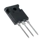
IXGH 28N60BD1
IXGT 28N60BD1
VCES
IC25
VCE(sat)
= 600 V
= 40 A
= 2.0 V
Combi Pack
Symbol
Test Conditions
Maximum Ratings
VCES
TJ = 25°C to 150°C
600
V
VCGR
TJ = 25°C to 150°C; RGE = 1 MΩ
600
V
VGES
Continuous
±20
V
VGEM
Transient
±30
V
IC25
TC = 25°C
40
A
IC90
TC = 90°C
28
A
ICM
TC = 25°C, 1 ms
80
A
SSOA
(RBSOA)
VGE = 15 V, TVJ = 125°C, RG = 10 Ω
Clamped inductive load
PC
TC = 25°C
ICM = 56
@ 0.8 VCES
A
150
W
-55 ... +150
°C
150
°C
Tstg
-55 ... +150
°C
Md
Mounting torque (M3) TO-247
G
300
6
4
C (TAB)
C
G = Gate,
E = Emitter,
E
C = Collector,
TAB = Collector
Features
z
1.13/10 Nm/lb.in.
TO-247
TO-268
C (TAB)
TO-247 AD
(IXGH)
z
Maximum lead temperature for soldering
1.6 mm (0.062 in.) from case for 10 s
Weight
G
E
TJM
TJ
TO-268
(IXGT)
°C
z
g
g
z
International standard packages
IGBT and anti-parallel FRED in one
package
Low VCE(sat)
- for minimum on-state conduction
losses
MOS Gate turn-on
- drive simplicity
Applications
z
z
Symbol
Test Conditions
Characteristic Values
(TJ = 25°C, unless otherwise specified)
min. typ. max.
= 250 µA, VCE = VGE
VGE(th)
IC
ICES
VCE = VCES
VGE = 0 V
IGES
VCE = 0 V, VGE = ±20 V
VCE(sat)
IC
= IC90, VGE = 15 V
2.5
TJ = 25°C
TJ = 125°C
5.5
V
200
3
µA
mA
±100
nA
2.0
V
z
z
z
Advantages
z
z
z
z
© 2003 IXYS All rights reserved
AC motor speed control
DC servo and robot drives
DC choppers
Uninterruptible power supplies (UPS)
Switch-mode and resonant-mode
power supplies
Space savings (two devices in one
package)
Easy to mount with 1 screw
(isolated mounting screw hole)
Reduces assembly time and cost
High power density
DS98567A(08/03)
�IXGH 28N60BD1
IXGT 28N60BD1
Symbol
Test Conditions
Characteristic Values
(TJ = 25°C, unless otherwise specified)
min. typ. max.
gfs
IC = IC90; VCE = 10 V,
Pulse test, t ≤ 300 µs, duty cycle ≤ 2 %
15
Cies
Coes
VCE = 25 V, VGE = 0 V, f = 1 MHz
Cres
Qg
Qge
IC = IC90, VGE = 15 V, VCE = 0.5 VCES
Qgc
td(on)
Inductive load, TJ = 25°°C
tri
IC = IC90, VGE = 15 V, L = 100 µH,
VCE = 0.8 VCES, RG = Roff = 10 Ω
td(off)
tfi
Eoff
td(on)
tri
Eon
td(off)
tfi
Eoff
S
1500
pF
170
pF
40
pF
68
100
nC
15
30
nC
20
40
nC
15
Remarks: Switching times may increase
for VCE (Clamp) > 0.8 • VCES, higher TJ or
increased RG
25
= IC90, VGE = 15 V, L = 100 µH
VCE = 0.8 VCES, RG = Roff = 10 Ω
Remarks: Switching times may increase
for VCE (Clamp) > 0.8 • VCES, higher TJ or
increased RG
400
ns
260
400
ns
2
4
mJ
ns
25
ns
1
mJ
400
ns
400
ns
3
mJ
0.83 K/W
TO-247
Reverse Diode (FRED)
Symbol
ns
175
RthJC
RthCK
ns
15
Inductive load, TJ = 125°°C
IC
25
Test Conditions
0.25
TO-247 AD Outline
1
2
3
Dim.
Millimeter
Min.
Max.
A
4.7
5.3
A1
2.2
2.54
A2
2.2
2.6
b
1.0
1.4
b1
1.65
2.13
b2
2.87
3.12
C
.4
.8
D
20.80 21.46
E
15.75 16.26
e
5.20
5.72
L
19.81 20.32
L1
4.50
∅P 3.55
3.65
Q
5.89
6.40
R
4.32
5.49
S
6.15 BSC
Terminals:
1 - Gate
2 - Collector
3 - Emitter
Tab-Collector
Inches
Min. Max.
.185 .209
.087 .102
.059 .098
.040 .055
.065 .084
.113 .123
.016 .031
.819 .845
.610 .640
0.205 0.225
.780 .800
.177
.140 .144
0.232 0.252
.170 .216
242 BSC
TO-268 Outline
K/W
Characteristic Values
(TJ = 25°C, unless otherwise specified)
min. typ. max.
VF
IF = IC90, VGE = 0 V,
TJ = 150°C
Pulse test, t ≤ 300 µs, duty cycle d ≤ 2 % TJ = 25°C
IRM
t rr
IF = IC90, VGE = 0 V, -diF/dt = 100 A/µs
VR = 100 V
IF = 1 A; -di/dt = 100 A/µs; VR = 30 V
TJ = 100°C
TJ = 25°C
RthJC
1.6
2.5
6
100
25
V
V
Terminals: 1 - Gate
3 - Emitter
2 - Collector
Tab - Collector
A
ns
ns
1 K/W
IXYS reserves the right to change limits, test conditions, and dimensions.
IXYS MOSFETs and IGBTs are covered by one or more
of the following U.S. patents:
4,835,592 4,881,106 5,017,508 5,049,961 5,187,117 5,486,715 6,306,728B1 6,259,123B1 6,306,728B1
4,850,072 4,931,844 5,034,796 5,063,307 5,237,481 5,381,025 6,404,065B1 6,162,665
6,534,343
�IXGH 28N60BD1
IXGT 28N60BD1
Fig. 1. Output Characte ristics
@ 25 Deg. C
Fig. 2. Extended Output Characte ristics
@ 25 de g. C
240
60
VGE = 15V
13V
11V
9V
200
40
I C - Amperes
I C - Amperes
50
VGE = 15V
30
7V
20
10
13V
160
11V
120
9V
80
40
7V
5V
5V
0
0
0.5
1
1.5
2
2.5
3
0
V C E - Volts
Fig. 3. Output Characteristics
@ 125 Deg. C
4
6
8
10
12
V C E - Volts
16
18
20
1.6
VGE = 15V
13V
11V
9V
V GE = 15V
1.5
V C E (sat)- Normalized
50
40
30
7V
20
I C = 56A
1.4
1.3
1.2
I C = 28A
1.1
1.0
0.9
I C = 14A
10
0.8
5V
0
0.7
0.5
1
1.5
2
2.5
3
-50
3.5
-25
V CE - Volts
0
25
50
75
100
125
TJ - Degrees Centigrade
Fig. 5. Collector-to-Em itter Voltage
vs. Gate-to-Em itter voltage
Fig. 6. Input Adm ittance
5
90
TJ = 25ºC
80
4.5
70
4
I C = 56A
28A
14A
3.5
3
I C - Amperes
VC E - Volts
14
Fig. 4. De pende nce of V CE(sat) on
Tem perature
60
I C - Amperes
2
2.5
60
50
40
30
2
20
1.5
10
1
0
6
7
8
9
10
11
12
13
V G E - Volts
© 2003 IXYS All rights reserved
14
15
16
17
TJ = 125ºC
25ºC
-40ºC
4
5
6
7
V G E - Volts
8
9
150
�IXGH 28N60BD1
IXGT 28N60BD1
Fig. 7. Transconductance
Fig. 8. Dependence of Eoff on RG
10.0
35
8.0
I C = 56A
E off - milliJoules
g f s - Siemens
25
TJ = 125ºC
VGE = 15V
VCE = 480V
9.0
TJ = -40ºC
25ºC
125ºC
30
20
15
10
7.0
6.0
5.0
I C = 28A
4.0
3.0
5
I C = 14A
2.0
0
1.0
0
10
20
30
40
50
60
70
80
90
10
I C - Amperes
30
70
90
110
R G - Ohms
130
150
Fig. 10. Dependence of Eoff on
Tem perature
Fig. 9. Dependence of Eoff on IC
8.0
8.0
R G = 10Ω
R G = 82Ω - - - VGE = 15V
VCE = 480V
6.0
R G = 10Ω
R G = 82Ω - - - VGE = 15V
VCE = 480V
7.0
6.0
E off - milliJoules
7.0
E off - MilliJoules
50
I C = 56A
5.0
5.0
4.0
4.0
TJ = 125ºC
I C = 28A
3.0
3.0
2.0
2.0
TJ = 25ºC
1.0
1.0
0.0
0.0
25
10
20
30
40
50
45
55
65
75
I C = 14A
85
95
105 115
125
60
I C - Amperes
TJ - Degrees Centigrade
Fig. 11. Dependence of Sw itching
Tim e on RG
Fig. 12. Dependence of Sw itching
Tim e on IC
600
1200
td(off)
tfi - - - - - -
1000
TJ = 125ºC
VGE = 15V
VCE = 480V
900
800
700
600
I C = 14A
I C = 56A
500
400
I C = 28A
300
td(off)
tfi - - - - - -
550
Switching Time - nanosecond
1100
Switching Time - nanosecond
35
R G = 10Ω
VGE = 15V
VCE = 480V
500
450
400
TJ = 125ºC
350
300
250
TJ = 25ºC
200
150
200
10
30
50
70
90
R G - Ohms
110
130
150
10
20
30
40
50
60
I C - Amperes
IXYS reserves the right to change limits, test conditions, and dimensions.
IXYS MOSFETs and IGBTs are covered by one or more
of the following U.S. patents:
4,835,592 4,881,106 5,017,508 5,049,961 5,187,117 5,486,715 6,306,728B1 6,259,123B1 6,306,728B1
4,850,072 4,931,844 5,034,796 5,063,307 5,237,481 5,381,025 6,404,065B1 6,162,665
6,534,343
�IXGH 28N60BD1
IXGT 28N60BD1
Fig. 13. Dependence of Sw itching
Tim e on Tem perature
Fig. 14. Gate Charge
500
15
td(off)
tfi - - - - - R G = 10Ω
VGE = 15V
VCE = 480V
400
350
300
VCE = 300V
IC = 28A
IG = 10mA
12
I C = 56A
VG E - Volts
Switching Time - nanosecond
450
I C = 14A
9
6
I C = 28A
250
3
200
I C = 56A
150
0
25
35
45
55
65
75
85
95
105 115 125
0
10
20
TJ - Degrees Centigrade
30
40
50
60
70
Q G - nanoCoulombs
Fig. 15. Capacitance
10000
Capacitance - p F
f = 1 MHz
C ies
1000
C oes
100
C res
10
0
5
10
15
20
25
30
35
40
V C E - Volts
Fig. 16. Maxim um Transient Therm al Resistance
R (th) J C - (ºC/W)
1
0.5
0.1
1
10
100
Pulse Width - milliseconds
© 2003 IXYS All rights reserved
1000
�60
A
TVJ= 100°C
A
nC
50
IF
30
1000 T = 100°C
VJ
800
Qr
25
IF= 60A
IF= 30A
IF= 60A
IF= 30A
IRM
40
20
TVJ=150°C
30
600
15
TVJ=100°C
400
20
10
TVJ=25°C
200
10
0
0
1
0
100
3 V
2
5
0
A/µs 1000
-diF/dt
VF
Fig. 12 Forward current IF versus VF
Fig. 13 Reverse recovery charge Qr
2.0
90
IF= 60A
IF= 30A
IRM
1.00
µs
VFR
tfr
0.75
tfr
80
1.0
600 A/µs
800 1000
-diF/dt
400
Fig. 14 Peak reverse current IRM
V
VFR
15
trr
Kf
200
20 TVJ= 100°C
TVJ= 100°C
ns
1.5
0
10
0.50
5
0.25
70
0.5
Qr
0.0
60
0
40
80
120 °C 160
0
0
200
TVJ
400
600
800 1000
A/µs
0
200
400
-diF/dt
Fig. 15 Dynamic parameters Qr, IRM
Fig. 16 Recovery time trr versus -diF/dt
1
K/W
0.00
600 A/µs
800 1000
diF/dt
Fig. 17 Peak forward voltage VFR and
tfr
Constants for ZthJC calculation:
i
1
2
0.1
Rthi (K/W)
ti (s)
0.502
0.193
0.0052
0.0003
ZthJC
0.01
0.001
0.00001
DSEP 29-06
0.0001
0.001
0.01
s
0.1
1
t
Fig. 18 Transient thermal resistance junction to case
IXYS reserves the right to change limits, test conditions, and dimensions.
IXYS MOSFETs and IGBTs are covered by one or more
of the following U.S. patents:
4,835,592 4,881,106 5,017,508 5,049,961 5,187,117 5,486,715 6,306,728B1 6,259,123B1 6,306,728B1
4,850,072 4,931,844 5,034,796 5,063,307 5,237,481 5,381,025 6,404,065B1 6,162,665
6,534,343
�