HiPerFASTTM IGBT
IXGH50N60A
VCES
IXGH50N60AS IC25
VCE(sat)
tfi
Surface Mountable
Symbol
Test Conditions
VCES
TJ = 25°C to 150°C
600
V
VCGR
TJ = 25°C to 150°C; RGE = 1 MΩ
600
V
VGES
Continuous
±20
V
VGEM
Transient
±30
V
I C25
TC = 25°C
75
A
I C90
TC = 90°C
50
A
I CM
TC = 25°C, 1 ms
200
A
SSOA
(RBSOA)
VGE = 15 V, T VJ = 125°C, RG = 10 Ω
Clamped inductive load, L = 30 µH
ICM = 100
@ 0.8 VCES
A
PC
TC = 25°C
250
W
-55 ... +150
°C
TJM
150
°C
Tstg
-55 ... +150
°C
300
°C
Maximum Lead and Tab temperature for soldering
1.6 mm (0.062 in.) from case for 10 s
Md
Mounting torque, TO-247 AD
Weight
Symbol
IC
= 250 µA, VGE = 0 V
600
VGE(th)
IC
= 250 µA, VCE = VGE
2.5
ICES
VCE = 0.8 • VCES
VGE = 0 V
I GES
VCE = 0 V, VGE = ±20 V
VCE(sat)
IC
= IC90, VGE = 15 V
© 1996 IXYS All rights reserved
4
6
g
g
Characteristic Values
(TJ = 25°C, unless otherwise specified)
min. typ. max.
BVCES
TJ = 25°C
TJ = 125°C
C (TAB)
G
E
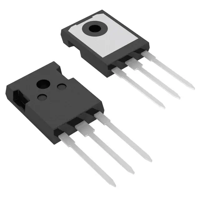
TO-247 AD
(50N60A)
C (TAB)
1.13/10 Nm/lb.in.
TO-247 SMD
TO-247 AD
Test Conditions
TO-247 SMD
(50N60AS)
Maximum Ratings
TJ
= 600 V
=
75 A
= 2.7 V
= 275 ns
V
5
G
C
G = Gate,
E = Emitter,
E
C = Collector,
TAB = Collector
Features
l
International standard packages
JEDEC TO-247 SMD surface
mountable and JEDEC TO-247 AD
l
High frequency IGBT
l
High current handling capability
l
2nd generation HDMOSTM process
l
MOS Gate turn-on
- drive simplicity
Applications
l
AC motor speed control
l
DC servo and robot drives
DC choppers
l
Uninterruptible power supplies (UPS)
l
Switch-mode and resonant-mode
power supplies
l
V
200
1
µA
mA
±100
nA
2.7
V
Advantages
High power density
l
Suitable for surface mounting
l
Switching speed for high frequency
applications
l
Easy to mount with 1 screw, TO-247
(insulated mounting screw hole)
l
92797H(9/96)
�IXGH50N60A
Symbol
Test Conditions
gfs
I C = I C90; VCE = 10 V,
Pulse test, t ≤ 300 µs, duty cycle ≤ 2 %
25
35
S
∅P
4000
pF
430
pF
Cres
100
pF
Qg
200
Q ge
VCE = 25 V, VGE = 0 V, f = 1 MHz
IC = IC90, VGE = 15 V, VCE = 0.5 VCES
Qgc
td(on)
Inductive load, T J = 25°°C
tri
Eoff
IC = IC90, VGE = 15 V, L = 30 µH,
VCE = 0.8 VCES , RG = Roff = 2.7 Ω
Remarks: Switching times may increase
for VCE (Clamp) > 0.8 • VCES, higher
TJ or increased RG
td(on)
Inductive load, TJ = 125°°C
tri
IC = IC90, VGE = 15 V, L = 30 µH
td(off)
tfi
Eon
VCE = 0.8 V CES, RG = Roff = 2.7 Ω
td(off)
Remarks: Switching times may increase
for VCE (Clamp) > 0.8 • VCES ,
higher TJ or increased RG
tfi
Eoff
TO-247 AD Outline
Characteristic Values
(TJ = 25°C, unless otherwise specified)
min. typ. max.
Cies
Coes
IXGH50N60AS
nC
35
50
nC
80
100
nC
50
ns
210
ns
200
275
ns
400
ns
4.8
mJ
50
ns
240
ns
3
mJ
280
ns
600
ns
9.6
mJ
e
Dim.
Millimeter
Min. Max.
A
4.7
5.3
A1
2.2
2.54
A2
2.2
2.6
b
1.0
1.4
b1
1.65
2.13
b2
2.87
3.12
C
.4
.8
D
20.80 21.46
E
15.75 16.26
e
5.20
5.72
L
19.81 20.32
L1
4.50
∅P 3.55
3.65
Q
5.89
6.40
R
4.32
5.49
S
6.15 BSC
Inches
Min. Max.
.185 .209
.087 .102
.059 .098
.040 .055
.065 .084
.113 .123
.016 .031
.819 .845
.610 .640
0.205 0.225
.780 .800
.177
.140 .144
0.232 0.252
.170 .216
242 BSC
TO-247 SMD Outline
0.50 K/W
RthJC
RthCK
250
0.25
K/W
Min. Recommended Footprint (Dimensions in inches and (mm))
1. Gate
2. Collector
Dim.
A
A1
A2
b
b1
C
D
E
e
L
L1
L2
L3
L4
ØP
Q
R
S
3. Emitter
4. Collector
Millimeter
Min.
Max.
4.83
5.21
2.29
2.54
1.91
2.16
Inches
Min. Max.
.190
.205
.090
.100
.075
.085
1.14
1.91
0.61
20.80
15.75
5.45
4.90
2.70
2.10
0.00
1.90
3.55
5.59
1.40
2.13
0.80
21.34
16.13
BSC
5.10
2.90
2.30
0.10
2.10
3.65
6.20
.045
.075
.024
.819
.620
.215
.193
.106
.083
.00
.075
.140
.220
.055
.084
.031
.840
.635
BSC
.201
.114
.091
.004
.083
.144
.244
4.32
6.15
4.83
BSC
.170
.242
.190
BSC
IXYS reserves the right to change limits, test conditions, and dimensions.
IXYS MOSFETS and IGBTs are covered by one or more of the following U.S. patents:
4,835,592
4,850,072
4,881,106
4,931,844
5,017,508
5,034,796
5,049,961
5,063,307
5,187,117
5,237,481
5,486,715
5,381,025
�IXGH50N60A
Fig. 1 Saturation Characteristics
Fig. 2
350
80
70
300
IC - Amperes
60
IC - Amperes
Output Characterstics
VGE = 15V
T J = 25°C
VGE = 15V
50
13V
11V
9V
7V
5V
40
30
20
7V
100
0
3
9V
150
0
2
4
5
5V
0
2
4
6
VCE - Volts
Fig. 4
10 12 14 16 18 20
Temperature Dependence
of Output Saturation Voltage
1.5
10
T J = 25°C
9
1.4
VCE(sat) - Normalized
8
7
VCE - Volts
8
VCE - Volts
Fig. 3 Collector-Emitter Voltage
vs. Gate-Emitter Voltage
6
5
4
3
IC = 40A
2
1
4
5
6
7
8
IC = 80A
1.3
1.2
1.1
IC = 40A
1.0
0.9
IC = 20A
0.8
IC = 20A
0
0.7
-50
9 10 11 12 13 14 15
-25
0
VGE - Volts
25
50
75
100 125 150
TJ - Degrees C
Fig. 5 Input Admittance
Fig. 6
Temperature Dependence of
Breakdown and Threshold Voltage
1.2
80
VCE = 100V
VGE(th) @ 250µA
BV / VCE(sat) - Normalized
70
60
IC - Amperes
T J = 25°C
200
50
1
13V
11V
250
10
0
IXGH50N60AS
50
40
30
20
TJ = 25°C
10
1.1
1.0
0.9
BVCES @ 3mA
0.8
0.7
0.6
T J = 125°C
0
0
1
2
3
4
5
6
VGE - Volts
© 1996 IXYS All rights reserved
7
8
9
10
0.5
-50
-25
0
25
50
75
TJ - Degrees C
100 125 150
�IXGH50N60A
Fig.7 Gate Charge
15
IXGH50N60AS
Fig.8 Turn-Off Safe Operating Area
100
IC = 40A
V CE = 500V
10
IC - Amperes
VGE - Volts
12
9
6
T J = 125°C
dV/dt < 3V/ns
1
0.1
3
0.01
0
0
50
100
150
200
250
0
100
Total Gate Charge - (nC)
200
300
400
500
600
700
VCE - Volts
Fig.9 Capacitance Curves
4500
Capacitance - pF
4000
Cies
3500
3000
2500
2000
1500
Coes
1000
Cres
500
0
0
5
10
15
20
25
VCE - Volts
Fig.10 Transient Thermal Impedance
1
ZthJC (K/W)
D=0.5
0.1
D=0.2
D=0.1
D=0.05
D=0.02
D = Duty Cycle
0.01 D=0.01
Single Pulse
0.001
0.00001
0.0001
0.001
0.01
0.1
1
10
Pulse Width - seconds
G50N60 2 JNB
IXYS reserves the right to change limits, test conditions, and dimensions.
IXYS MOSFETS and IGBTs are covered by one or more of the following U.S. patents:
4,835,592
4,850,072
4,881,106
4,931,844
5,017,508
5,034,796
5,049,961
5,063,307
5,187,117
5,237,481
5,486,715
5,381,025
�