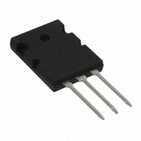
ADVANCE TECHNICAL INFORMATION
HiPerFASTTM IGBT
Lightspeed 2TM Series
Symbol
Test Conditions
VCES
TJ = 25°C to 150°C
600
V
VCGR
TJ = 25°C to 150°C; RGE = 1 MΩ
600
V
VGES
Continuous
± 20
V
VGEM
Transient
± 30
V
IC25
TC = 25°C (limited by leads)
Maximum Ratings
IC110
ICM
SSOA
VGE = 15 V, TVJ = 125°C, RG = 4.7 Ω
(RBSOA)
Clamped inductive load @ VCE ≤ 600 V
PC
TC = 25°C
75
A
TC = 110°C (die limit)
120
A
TC = 25°C, 1 ms
500
A
ICM = 200
A
830
W
-55 ... +150
°C
TJM
150
°C
Tstg
-55 ... +150
°C
2500
3000
V~
V~
20..120/4.5..25
N/ib
TJ
VISOL
50/60 Hz, RMS, t = 1minute
IISOL < 1 mA
t = 20 seconds
FC
Clamping force
TL
Maximum lead temperature for soldering (Note 3)
300
°C
TSOLD
Plastic body for 10 seconds
260
°C
10
5
g
g
Weight
TO-264
PLUS247
Symbol
Test Conditions
BVCES
VGE(th)
IC
IC
ICES
VCE = VCES
VGE = 0 V
Characteristic Values
(TJ = 25°C unless otherwise specified)
Min. Typ. Max.
= 1 mA, VGE = 0 V
= 500 μA, VCE = VGE
IGES
VCE = 0 V, VGE = ± 20 V
VCE(sat)
IC = IT, VGE = 15 V
Note 1
© 2005 IXYS All rights reserved
VCES
IC110
VCE(sat)
tfi(typ)
IXGK 120N60C2
IXGX 120N60C2
600
3.0
TJ = 125°C
TJ = 25°C
TJ = 125°C
2.1
2.0
5.0
V
V
100
2
μA
mA
± 200
nA
2.5
V
V
= 600 V
= 120 A
= 2.5 V
= 45 ns
TO-264(IXGK)
G
C
(TAB)
E
PLUS247(IXGX)
G
C
G = Gate
E = Emitter
E
(TAB)
C = Collector
Tab = Collector
Features
z
Very high frequency IGBT
z
Square RBSOA
z
High current handling capability
z
MOS Gate turn-on
- drive simplicity
Applications
z
Uninterruptible power supplies (UPS)
z
Switched-mode and resonant-mode
power supplies
z
AC motor speed control
z
DC servo and robot drives
z
DC choppers
Advantages
z
High power density
z
Very fast switching speeds for high
frequency applications
z
High power surface mountable
packages
DS99515 (12/05)
�IXGK 120N60C2
IXGX 120NC60C2
Symbol
gfs
Test Conditions
Characteristic Values
(TJ = 25°C unless otherwise specified)
Min. Typ. Max.
IC = 60 A; VCE = 10 V, Note 1
50
50
Cies
Coes
Cres
VCE = 25 V, VGE = 0 V, f = 1 MHz
Qg
Qge
Qgc
td(on)
tri
td(off)
tfi
IC = IT, VGE = 15 V, VCE = 0.5 VCES
75
S
11
nF
680
190
pF
pF
350
nC
72
131
nC
nC
18
ns
Inductive load, TJ = 25°C
25
ns
IC = 80 A, VGE = 15 V
95
VCE = 400 V, RG = Roff = 1.0 Ω
150
ns
45
ns
Eoff
0.9
td(on)
tri
Eon
td(off)
tfi
Eoff
18
25
1.6
130
85
1.5
ns
ns
mJ
ns
ns
mJ
0.15
0.15 K/W
K/W
Inductive load, TJ = 125°C
IC = 80 A, VGE = 15 V
VCE = 400 V, RG = Roff = 1.0 Ω
RthJC
RthJC
1.6
mJ
TO-264 AA Outline
Pins:1-Gate 2- Drain
3 - Source Tab - Drain
Dim.
Millimeter
Min.
Max.
A
A1
A2
b
b1
b2
c
D
E
e
J
K
L
L1
P
Q
Q1
R
R1
S
T
4.82
5.13
2.54
2.89
2.00
2.10
1.12
1.42
2.39
2.69
2.90
3.09
0.53
0.83
25.91 26.16
19.81 19.96
5.46 BSC
0.00
0.25
0.00
0.25
20.32 20.83
2.29
2.59
3.17
3.66
6.07
6.27
8.38
8.69
3.81
4.32
1.78
2.29
6.04
6.30
1.57
1.83
Inches
Min.
Max.
.190
.202
.100
.114
.079
.083
.044
.056
.094
.106
.114
.122
.021
.033
1.020
1.030
.780
.786
.215 BSC
.000
.010
.000
.010
.800
.820
.090
.102
.125
.144
.239
.247
.330
.342
.150
.170
.070
.090
.238
.248
.062
.072
PLUS 247TM (IXGX) Outline
Note: 1. Pulse test, t ≤ 300 μs, duty cycle ≤ 2 %;
2. Test current IT = 100 A;
3. Temperature measured at 1.6 mm (0.062 in.) from case for 10 seconds
Terminals: 1 - Gate
2 - Drain (Collector)
3 - Source (Emitter)
4 - Drain (Collector)
Dim.
A
A1
A2
b
b1
b2
C
D
E
e
L
L1
Q
R
Millimeter
Min. Max.
4.83
5.21
2.29
2.54
1.91
2.16
1.14
1.40
1.91
2.13
2.92
3.12
0.61
0.80
20.80 21.34
15.75 16.13
5.45 BSC
19.81 20.32
3.81
4.32
5.59
6.20
4.32
4.83
IXYS reserves the right to change limits, test conditions, and dimensions.
IXYS MOSFETs and IGBTs are covered by 4,835,592
one or more of the following U.S. patents: 4,850,072
4,881,106
4,931,844
5,017,508
5,034,796
5,049,961
5,063,307
5,187,117
5,237,481
5,381,025
5,486,715
6,162,665
6,259,123 B1
6,306,728 B1
6,404,065 B1
6,534,343
6,583,505
6,683,344
6,710,405B2
6,710,463
6,727,585
6,759,692
6771478 B2
Inches
Min. Max.
.190 .205
.090 .100
.075 .085
.045 .055
.075 .084
.115 .123
.024 .031
.819 .840
.620 .635
.215 BSC
.780 .800
.150 .170
.220 0.244
.170 .190
�
