IXGK 50N60BD1
IXGX 50N60BD1
HiPerFASTTM
IGBT with Diode
VCES
IC25
VCE(sat)
tfi
Symbol
Test Conditions
Maximum Ratings
VCES
TJ = 25°C to 150°C
600
V
VCGR
TJ = 25°C to 150°C; RGE = 1 MW
600
V
VGES
Continuous
±20
V
VGEM
Transient
±30
V
IC25
TC = 25°C
75
A
IC90
TC = 90°C
50
A
ICM
TC = 25°C, 1 ms
200
A
ICM = 100
A
SSOA
VGE = 15 V, TVJ = 125°C, RG = 10 W
(RBSOA)
Clamped inductive load, L = 30 mH
PC
TC = 25°C
@ 0.8 VCES
300
W
-55 ... +150
°C
TJM
150
°C
Tstg
-55 ... +150
°C
TJ
Md
Mounting torque, TO-247 AD
Weight
TO-264
TO-268
1.13/10 Nm/lb.in.
Maximum lead temperature for soldering
1.6 mm (0.062 in.) from case for 10 s
Symbol
Test Conditions
g
g
300
°C
Characteristic Values
(TJ = 25°C, unless otherwise specified)
Min. Typ. Max.
BVCES
IC
= 1 mA, VGE = 0 V
500
VGE(th)
IC
= 500 mA, VCE = VGE
2.5
ICES
VCE = VCES
VGE = 0 V
IGES
VCE = 0 V, VGE = ±20 V
VCE(sat)
IC
TJ = 25°C
TJ = 125°C
= IC90, VGE = 15 V
IXYS reserves the right to change limits, test conditions, and dimensions.
© 2000 IXYS All rights reserved
10
5
V
5.5
V
650
5
mA
mA
±100
nA
2.3
V
= 600 V
=
75 A
= 2.3 V
=
85 ns
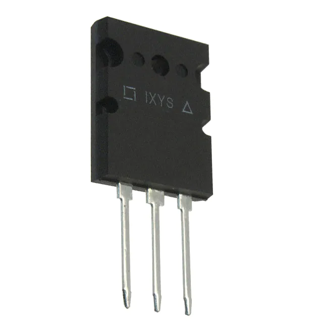
TO-264 AA
(IXGK)
(TAB)
G
C
E
PLUS247
(IXGX)
G = Gate
E = Emitter
C = Collector
Tab = Collector
Features
• International standard packages
JEDEC TO-268 and PLUS247 (holeless TO-247)
• High frequency IGBT and antparallel
FRED in one package
• New generation HDMOSTM process
• High current handling capability
• MOS Gate turn-on fordrive simplicity
• Fast Recovery Epitaxial Diode
(FRED) with soft recovery and low IRM
Applications
• AC motor speed control
• DC servo and robot drives
• DC choppers
• Uninterruptible power supplies (UPS)
• Switch-mode and resonant-mode
power supplies
Advantages
• Space savings (two devices on one
package
• Easy to mount with 1 screw
98516B (7/00)
1-5
�IXGK 50N60BD1
IXGX 50N60BD1
Symbol
Test Conditions
Characteristic Values
(TJ = 25°C, unless otherwise specified)
Min. Typ. Max.
35
S
4000
340
pF
pF
C res
100
pF
Qg
Qge
110
30
nC
nC
35
nC
gfs
C ies
Coes
IC = IC90; VCE = 10 V,
Pulse test, t £ 300 ms, duty cycle £ 2 %
VCE = 25 V, VGE = 0 V, f = 1 MHz
IC = IC90, VGE = 15 V, VCE = 0.5 VCES
25
Qgc
TO-264 AA Outline
Dim.
td(on)
t ri
td(off)
tfi
Eoff
td(on)
t ri
Eon
td(off)
tfi
Inductive load, TJ = 25°C
IC = IC90, VGE = 15 V, L = 100 mH,
VCE = 0.8 VCES, RG = Roff = 2.7 W
Remarks: Switching times may increase for VCE
(Clamp) > 0.8 • VCES, higher TJ or increased RG
Inductive load, TJ = 125°C
IC = IC90, VGE = 15 V, L = 100 mH
VCE = 0.8 VCES, RG = Roff = 2.7 W
Remarks: Switching times may increase for VCE
(Clamp) > 0.8 • VCES, higher TJ or increased RG
Eoff
RthJC
RthCK
TO-264 package
Reverse Diode (FRED)
Test Conditions
VF
IF = IC90, VGE = 0 V,
Pulse test, t £ 300 ms, duty cycle d 22 %
IRM
IF = IC90, VGE = 0 V, -diF/dt = 100 A/ms
VR = 100 V
IF = 1 A; -di/dt = 200 A/ms; VR = 30 V
RthJC
© 2000 IXYS All rights reserved
ns
50
ns
200
85
150
ns
150
ns
ns
1.5
mJ
50
60
3
200
175
ns
ns
mJ
ns
ns
2.5
mJ
0.15
0.42 K/W
K/W
A
A1
A2
b
b1
b2
c
D
E
e
J
K
L
L1
P
Q
Q1
R
R1
S
T
4.82
2.54
2.00
1.12
2.39
2.90
0.53
25.91
19.81
5.46
0.00
0.00
20.32
2.29
3.17
6.07
8.38
3.81
1.78
6.04
1.57
5.13
2.89
2.10
1.42
2.69
3.09
0.83
26.16
19.96
BSC
0.25
0.25
20.83
2.59
3.66
6.27
8.69
4.32
2.29
6.30
1.83
Inches
Min.
Max.
.190
.202
.100
.114
.079
.083
.044
.056
.094
.106
.114
.122
.021
.033
1.020
1.030
.780
.786
.215 BSC
.000
.010
.000
.010
.800
.820
.090
.102
.125
.144
.239
.247
.330
.342
.150
.170
.070
.090
.238
.248
.062
.072
PLUS247TM (IXGX)
Characteristic Values
(TJ = 25°C, unless otherwise specified)
min. typ. max.
Symbol
t rr
50
Millimeter
Min.
Max.
2
35
2.5
V
2.5
175
50
A
ns
ns
Dim.
0.65 K/W
A
A1
A2
b
b1
b2
C
D
E
e
L
L1
Q
R
Millimeter
Min. Max.
4.83
5.21
2.29
2.54
1.91
2.16
1.14
1.40
1.91
2.13
2.92
3.12
0.61
0.80
20.80 21.34
15.75 16.13
5.45 BSC
19.81 20.32
3.81
4.32
5.59
6.20
4.32
4.83
IXYS MOSFETS and IGBTs are covered by one or more of the following U.S. patents:
4,835,592
4,881,106
5,017,508
5,049,961
5,187,117
5,486,715
4,850,072
4,931,844
5,034,796
5,063,307
5,237,481
5,381,025
Inches
Min. Max.
.190 .205
.090 .100
.075 .085
.045 .055
.075 .084
.115 .123
.024 .031
.819 .840
.620 .635
.215 BSC
.780 .800
.150 .170
.220 .244
.170 .190
2-5
�IXGK 50N60BD1
IXGX 50N60BD1
100
TJ = 25°C
7V
60
40
20
11V
VGE = 15V
13V
160
IC - Amperes
80
IC - Amperes
200
VGE = 15V
13V
11V
9V
TJ = 25°C
9V
120
7V
80
40
5V
5V
0
0
0
1
2
3
4
5
0
2
4
VCE - Volts
8
Figure 2. Extended Output Characteristics
100
1.6
TJ = 125°C V = 15V
GE
13V
11V
VGE = 15V
9V
VCE (sat) - Normalized
80
7V
60
40
5V
20
0
0
1
2
3
4
1.2
IC = 50A
1.0
IC = 25A
0.8
0.6
0.4
25
5
IC = 100A
1.4
50
75
VCE - Volts
100
125
150
TJ - Degrees C
Figure 3. Saturation Voltage Characteristics
Figure 4. Temperature Dependence of VCE(sat)
10000
100
f = 1Mhz
VCE = 10V
Ciss
Capacitance - pF
80
IC - Amperes
10
VCE - Volts
Figure 1. Saturation Voltage Characteristics
IC - Amperes
6
60
40
TJ = 25°C
TJ = 125°C
1000
Coss
100
Crss
20
10
0
0
2
4
6
VGE - Volts
Figure 5. Admittance Curves
© 2000 IXYS All rights reserved
8
10
0
5
10
15
20
25
30
35
40
VCE-Volts
Figure 6. Capacitance Curves
3-5
�IXGK 50N60BD1
IXGX 50N60BD1
6
12
E(ON)
10
4
8
E(OFF)
3
6
2
4
1
12
TJ = 125°C
E(ON)
5
4
8
E(ON)
3
6
20
40
60
80
4
E(OFF)
2
E(ON)
0
E(OFF)
IC = 50A
2
1
2
0
10
E(OFF)
IC = 100A
IC =25A
0
0
100
E(OFF) - millijoules
RG = 4.7�
E(OFF) - milliJoules
E(ON) - millijoules
5
6
E(ON) - millijoules
TJ = 125°C
0
0
10
20
30
40
50
60
RG - Ohms
IC - Amperes
Figure 7. Dependence of EON and EOFF on IC.
Figure 8. Dependence of EON and EOFF on RG.
600
16
IC =25A
VCE = 250V
100
IC - Amperes
VGE - Volts
12
8
TJ = 125°C
10
RG = 6.2 �
dV/dt < 5V/ns
1
4
0.1
0
0
20
40
60
80
100
120
0
100
200
300
400
500
600
VCE - Volts
Qg - nanocoulombs
Figure 9. Gate Charge
Figure 10. Turn-off Safe Operating Area
ZthJC (K/W)
1
0.1
D=0.5
D=0.2
0.01
D=0.1
D=0.05
D=0.02
D = Duty Cycle
D=0.01
Single pulse
0.001
0.00001
0.0001
0.001
0.01
0.1
1
Pulse Width - Seconds
Figure 11. IGBT Transient Thermal Resistance
© 2000 IXYS All rights reserved
4-5
�IXGK 50N60BD1
IXGX 50N60BD1
4000
160
A
140
IF
80
TVJ= 100°C
VR = 300V
nC
A
3000
120
TVJ= 25°C
60
IF=120A
IF= 60A
IF= 30A
Qr
100
TVJ=100°C
80
TVJ= 100°C
VR = 300V
IRM
2000
40
1000
20
IF=120A
IF= 60A
IF= 30A
TVJ=150°C
60
40
20
0
0
1
2
0
100
V
VF
Fig. 12. Forward current IF versus VF
Fig. 13. Reverse recovery charge Qr
versus -diF/dt
2.0
140
400
ms 1000
600 A/
800
-diF/dt
Fig.14. Peak reverse current IRM
versus -diF/dt
4
VFR
µs
tfr
3
tfr
120
1.0
200
V
VFR
15
trr
Kf
0
20
TVJ= 100°C
VR = 300V
ns
130
1.5
0
A/ms 1000
-diF/dt
IF=120A
IF= 60A
IF= 30A
110
10
2
5
1
I RM
100
0.5
Qr
90
0.0
80
0
40
80
120 °C 160
0
TVJ
200
400
0
800
A/
ms 1000
600
TVJ= 100°C
IF = 60A
0
200
400
-diF/dt
Fig. 15. Dynamic parameters Qr, IRM
versus TVJ
Fig. 16. Recovery time trr versus -diF/dt
1
0
ms 1000
600 A/
800
diF/dt
Fig. 17. Peak forward voltage VFR and
tfr versus diF/dt
Constants for ZthJC calculation:
K/W
i
0.1
1
2
3
ZthJC
Rthi (K/W)
ti (s)
0.324
0.125
0.201
0.0052
0.0003
0.0385
0.01
0.001
0.0001
0.00001
DSEP 60-06A
0.0001
0.001
0.01
s
0.1
1
t
Fig. 18. Transient thermal resistance junction to case
© 2000 IXYS All rights reserved
5-5
�