High Voltage IGBT with Diode
VCES
IC25
VCE(sat)
IXGQ 20N120B
IXGQ 20N120BD1
= 1200
= 40
= 3.4
= 160
tfi(typ)
V
A
V
ns
BD1
Maximum Ratings
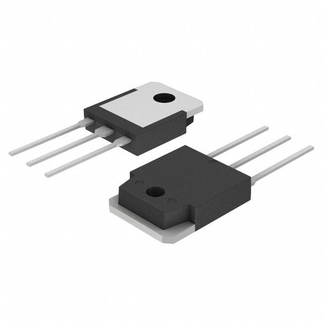
TO-3P (IXGQ)
Symbol
Test Conditions
VCES
TJ = 25°C to 150°C
1200
V
VCGR
TJ = 25°C to 150°C; RGE = 1 MΩ
1200
V
VGES
Continuous
±20
V
VGEM
Transient
±30
V
IC25
TC = 25°C
40
A
IC110
TC = 110°C
20
A
ICM
TC = 25°C, 1 ms
100
A
SSOA
(RBSOA)
VGE = 15 V, TJ = 125°C, RG = 10 Ω
Clamped inductive load
ICM = 40
@0.8 VCES
A
PC
TC = 25°C
190
W
-55 ... +150
°C
z
TJM
150
°C
z
Tstg
-55 ... +150
°C
TJ
Md
Mounting torque
300
°C
6
g
Characteristic Values
(TJ = 25°C, unless otherwise specified)
min. typ. max.
IC
ICES
VCE = VCES
VGE = 0 V
IGES
VCE = 0 V, VGE = ±20 V
VCE(sat)
IC
= 20A, VGE = 15 V
Note 2
© 2003 IXYS All rights reserved
2.5
20N120B
20N120BD1
TJ=125°C
2.9
2.8
5.0
V
25
50
µA
µA
±100
nA
3.4
V
V
(TAB)
C = Collector
TAB = Collector
Features
z
International standard package
IGBT and anti-parallel FRED for
resonant power supplies
- Induction heating
- Rice cookers
MOS Gate turn-on
- drive simplicity
Fast Recovery Expitaxial Diode (FRED)
- soft recovery with low IRM
Advantages
z
z
= 250 µA, VCE = VGE
VGE(th)
E
G = Gate
E = Emitter
z
Weight
Test Conditions
C
1.13/10 Nm/lb.in.
Maximum lead temperature for soldering
1.6 mm (0.062 in.) from case for 10 s
Symbol
G
z
Saves space (two devices in one
package)
Easy to mount with 1 screw
(isolated mounting screw hole)
Reduces assembly time and cost
DS99136(12/03)
�IXGQ 20N120B
IXGQ 20N120BD1
Symbol
Test Conditions
gfs
IC = 20A; VCE = 10 V,
Note 2.
Characteristic Values
(TJ = 25°C, unless otherwise specified)
min. typ. max.
12
Cies
20N120B
Coes
VCE = 25 V, VGE = 0 V, f = 1 MHz
20N120BD1
Cres
Qg
IC = 20A, VGE = 15 V, VCE = 0.5 VCES
Qge
Qgc
16
S
1700
70
pF
pF
80
pF
23
pF
62
nC
9
nC
24
nC
td(on)
Inductive load, TJ = 25°°C
20
ns
tri
IC = 20 A; VGE = 15 V
VCE = 0.8 VCES; RG = Roff = 10 Ω
Note 1.
14
ns
td(off)
tfi
Eoff
td(on)
tri
Eon
td(off)
Inductive load, TJ = 125°°C
IC = 20A; VGE = 15 V
VCE = 0.8 VCES; RG = Roff = 10 Ω
Note 1
tfi
Eoff
RthJC
RthCK
(TO-247)
Reverse Diode (FRED)
270
380
160
2.1
320 n s
3.5 mJ
25
ns
18
ns
1.4
mJ
270
ns
360
4.5
ns
mJ
0.25
0.65 K/W
K/W
ns
Characteristic Values
(TJ = 25°C, unless otherwise specified)
min. typ. max.
Symbol
Test Conditions
IF
TC = 90°C
10
A
VF
IF = 10 A, VGE = 0 V
3.3
V
IRM
t rr
IF = 10 A; -diF/dt = 400 A/µs, VR = 600 V
VGE = 0 V; TJ = 125°C
t rr
IF = 1 A; -diF/dt = 100 A/µs; VR = 30 V, VGE = 0 V
14
120
A
ns
40
ns
2.5 K/W
RthJC
Notes:
TO-3P (IXGQ) Outline
1.
2.
Switching times may increase for VCE (Clamp) > 0.8 • VCES,
higher TJ or increased RG.
Pulse test, t ≤ 300 µs, duty cycle d ≤ 2 %
IXYS reserves the right to change limits, test conditions, and dimensions.
IXYS MOSFETs and IGBTs are covered by one or more
of the following U.S. patents:
4,835,592 4,881,106 5,017,508 5,049,961 5,187,117 5,486,715 6,306,728B1 6,259,123B1 6,306,728B1
4,850,072 4,931,844 5,034,796 5,063,307 5,237,481 5,381,025 6,404,065B1 6,162,665
6,534,343
�IXGQ 20N120B
IXGQ 20N120BD1
Fig. 1. Output Characteristics
@ 25 Deg. C
Fig. 2. Extende d Output Characteris tics
@ 25 deg. C
40
160
VGE = 15V
13V
11V
9V
I C - Amperes
30
VGE = 15V
140
13V
120
I C - Amperes
35
25
20
7V
15
11V
100
80
9V
60
10
40
5
20
7V
5V
5V
0
0
0.5
1
1.5
2
2.5
3
3.5
4
4.5
0
2
4
6
8
Fig. 3. Output Characteristics
@ 125 Deg. C
12
14
16
18
20
Fig. 4. Depende nce of V CE(sat) on
Tem perature
40
1.5
VGE = 15V
13V
11V
9V
30
VGE = 15V
1.4
I C = 40A
V C E (sat)- Normalized
35
I C - Amperes
10
V C E - Volts
V C E - Volts
25
20
7V
15
10
1.3
1.2
1.1
I C = 20A
1.0
0.9
I C = 10A
5
0.8
5V
0
0.7
0.5
1
1.5
2
2.5
3
3.5
4
4.5
-50
-25
0
V CE - Volts
Fig. 5. Colle ctor-to-Em itter Voltage
vs . Gate-to-Em iite r voltage
50
75
100
125
Fig. 6. Input Adm ittance
60
6.5
TJ = 25ºC
6
50
5
I C - Amperes
5.5
VC E - Volts
25
TJ - Degrees Centigrade
I C = 40A
20A
10A
4.5
4
3.5
40
30
20
3
2.5
TJ = 125ºC
25ºC
-40ºC
10
2
0
1.5
6
7
8
9
10
11
12
13
V G E - Volts
© 2003 IXYS All rights reserved
14
15
16
17
4
5
6
7
V G E - Volts
8
9
150
�IXGQ 20N120B
IXGQ 20N120BD1
Fig. 8. Dependence of Turn-off
Ene rgy Loss on RG
Fig. 7. Trans conductance
24
16
21
12
E off - milliJoules
g f s - Siemens
18
15
12
9
8
I C = 20A
6
4
3
2
0
0
10
20
30
40
50
I C = 40A
10
6
0
TJ = 125ºC
VGE = 15V
VCE = 960V
14
TJ = -40ºC
25ºC
125ºC
60
I C = 10A
10
30
50
70
I C - Amperes
Fig. 9. Dependence of Turn-Off
Ene rgy Loss on Ic
110
130
150
Fig. 10. De pende nce of Turn-off
Ene rgy Loss on Tem pe rature
14
14
R G = 10Ω
R G = 100Ω - - VGE = 15V
VCE = 960V
TJ = 125ºC
10
8
TJ = 125ºC
6
R G = 10Ω
R G = 100Ω - - VGE = 15V
VCE = 960V
12
E off - milliJoules
12
E off - MilliJoules
90
R G - Ohms
10
I C = 40A
8
6
I C = 20A
4
4
TJ = 25ºC
2
2
0
0
I C = 10A
10
15
20
25
30
35
25
40
35
45
I C - Amperes
Fig. 11. Dependence of Turn-off
Sw itching Tim e on RG
65
75
85
95
105 115 125
Fig. 12. Depe ndence of Turn-off
Sw itching Tim e on Ic
1400
550
td(off)
tfi - - - - - -
1200
Switching Time - nanoseconds
Switching Time - nanoseconds
55
TJ - Degrees Centigrade
TJ = 125ºC
VGE = 15V
VCE = 960V
1000
800
I C = 10A
I C = 40A
600
400
td(off)
tfi - - - - - -
500
R G = 10Ω
VGE = 15V
VCE = 960V
450
400
TJ = 125ºC
350
300
TJ = 25ºC
250
I C = 20A
200
200
10
30
50
70
90
110
130
150
R G - Ohms
10
15
20
25
30
35
40
I C - Amperes
IXYS reserves the right to change limits, test conditions, and dimensions.
IXYS MOSFETs and IGBTs are covered by one or more
of the following U.S. patents:
4,835,592 4,881,106 5,017,508 5,049,961 5,187,117 5,486,715 6,306,728B1 6,259,123B1 6,306,728B1
4,850,072 4,931,844 5,034,796 5,063,307 5,237,481 5,381,025 6,404,065B1 6,162,665
6,534,343
�IXGQ 20N120B
IXGQ 20N120BD1
Fig. 13. Dependence of Turn-off
Sw itching Tim e on Tem perature
Fig. 14. Gate Charge
15
td(off)
tfi - - - - - -
450
R G = 10Ω
VGE = 15V
VCE = 960V
400
350
VCE = 600V
IC = 20A
IG = 10mA
I C = 40A
12
VG E - Volts
Switching Time - nanoseconds
500
I C = 10A
I C = 20A
300
9
6
I C = 40A
3
250
200
0
25
35
45
55
65
75
85
95
105 115 125
0
10
20
TJ - Degrees Centigrade
30
40
50
60
70
Q G - nanoCoulombs
Fig. 15. Capacitance
10000
Capacitance - p F
f = 1 MHz
C ies
1000
100
C oes
C res
10
0
5
10
15
20
25
30
35
40
V C E - Volts
Fig. 16. Maxim um Transient Therm al Resistance
R (th) J C - (ºC/W)
1.0
0.5
0.1
1
10
100
Pulse Width - milliseconds
© 2003 IXYS All rights reserved
1000
�IXGQ 20N120B
IXGQ 20N120BD1
30
2000
IF
25
nC
20
1500
Qr
TVJ= 100°C
A VR = 600V
IRM
IF= 20A
IF= 10A
IF= 5A
TVJ=150°C
15
40
TVJ= 100°C
VR = 600V
A
30
1000
20
500
10
IF= 20A
IF= 10A
IF= 5A
TVJ=100°C
10
TVJ= 25°C
5
0
0
1
2
3
VF
0
100
4V
Fig. 17 Forward current IF versus VF
0
A/µs 1000
-diF/dt
Fig. 18 Reverse recovery charge Qr
versus -diF/dt
150
2.0
Kf
Qr
90
40
µs
tfr
VFR
80
0.8
40
0.4
100
0.0
0
tfr
IF= 20A
IF= 10A
IF= 5A
110
0.5
1.2
V
120
IRM
600 A/µs
800 1000
-diF/dt
TVJ= 100°C
IF = 10A
VFR
130
1.0
400
Fig. 19 Peak reverse current IRM
versus -diF/dt
140
trr
1.5
200
120
TVJ= 100°C
VR = 600V
ns
0
80
120 °C 160
0
0
200
400
600
TVJ
800 1000
A/µs
0
200
400
-diF/dt
Fig. 20 Dynamic parameters Qr, IRM
versus TVJ
Fig. 21 Recovery time trr versus -diF/dt
10
K/W
0.0
600 A/µs
800 1000
diF/dt
Fig. 22 Peak forward voltage VFR and
tfr versus diF/dt
Constants for ZthJC calculation:
i
1
1
2
3
ZthJC
Rthi (K/W)
ti (s)
1.449
0.558
0.493
0.0052
0.0003
0.017
0.1
0.01
0.001
0.00001
DSEP 8-12A
0.0001
0.001
0.01
s
0.1
1
t
Fig. 23 Transient thermal resistance junction to case
IXYS reserves the right to change limits, test conditions, and dimensions.
IXYS MOSFETs and IGBTs are covered by one or more
of the following U.S. patents:
4,835,592 4,881,106 5,017,508 5,049,961 5,187,117 5,486,715 6,306,728B1 6,259,123B1 6,306,728B1
4,850,072 4,931,844 5,034,796 5,063,307 5,237,481 5,381,025 6,404,065B1 6,162,665
6,534,343
�Disclaimer Notice - Information furnished is believed to be accurate and reliable. However, users should independently
evaluate the suitability of and test each product selected for their own applications. Littelfuse products are not designed for,
and may not be used in, all applications.Read complete Disclaimer Notice at www.littelfuse.com/disclaimer-electronics.
�