Advance Technical Information
High Voltage IGBTs
for Capacitor Discharge
Applications
IXGH2N250
IXGT2N250
VCES = 2500V
IC110 = 2A
VCE(sat) ≤ 3.1V
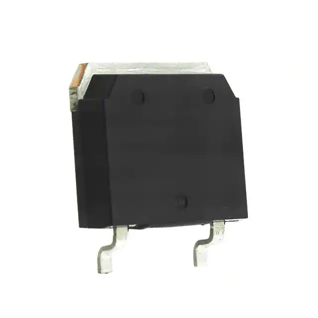
TO-247 (IXGH)
Symbol
Test Conditions
Maximum Ratings
VCES
TC = 25°C to 150°C
2500
VCGR
TJ = 25°C to 150°C, RGE = 1MΩ
2500
V
VGES
Continuous
± 20
V
VGEM
Transient
± 30
V
IC25
IC110
ICM
TC = 25°C
TC = 110°C
TC = 25°C, 1ms
5.5
2.0
13.5
A
A
A
SSOA
VGE = 15V, TVJ = 125°C, RG = 50Ω
ICM = 6
A
(RBSOA)
Clamped Inductive Load
VCE ≤ 2000
V
PC
TC = 25°C
32
W
-55 ... +150
°C
TJM
150
°C
Tstg
-55 ... +150
°C
300
260
°C
°C
1.13/10
Nm/lb.in.
6
4
g
g
TJ
TL
TSOLD
1.6mm (0.062 in.) from Case for 10s
Plastic Body for 10 seconds
Md
Mounting Torque (TO-247)
Weight
TO-247
TO-268
G
V
C
C (TAB)
E
TO-268 (IXGT)
G
E
C (TAB)
G = Gate
E = Emitter
C
= Collector
TAB = Collector
Features
z
z
Optimized for Low Conduction and
Switching Losses
International Standard Packages
Advantages
Symbol Test Conditions
(TJ = 25°C Unless Otherwise Specified)
Characteristic Values
Min.
Typ.
Max.
BVCES
IC = 250μA, VGE = 0V
2500
VGE(th)
IC = 250μA, VCE = VGE
3.0
ICES
VCE = 0.8 • VCES, VGE = 0V
IGES
VCE = 0V, VGE = ± 20V
VCE(sat)
IC = IC110, VGE = 15V, Note 1
© 2009 IXYS CORPORATION, All Rights Reserved
z
V
TJ = 125°C
TJ = 125°C
z
2.6
3.1
5.5
V
10
100
μA
μA
±100
nA
3.1
V
V
High Power Density
Low Gate Drive Requirement
Applications
z
z
z
Switched-Mode and Resonant-Mode
Power Supplies
Uninterruptible Power Supplies (UPS)
Capacitor Discharge Circuits
DS100162(06/09)
�IXGH2N250
IXGT2N250
Symbol
Test Conditions
(TJ = 25°C, Unless Otherwise Specified)
Characteristic Values
Min.
Typ.
Max.
gfs
IC = IC110, VCE = 10V, Note 1
0.7
Cies
Coes
Cres
TO-247 (IXGH) Outline
1.2
S
VCE = 25V, VGE = 0V, f = 1MHz
144
8.7
3.2
pF
pF
pF
Qg
Qge
Qgc
IC = IC110, VGE = 15V, VCE = 1000V
10.5
6.4
1.0
nC
nC
nC
td(on)
tr
Resistive Switching times, TJ = 25°C
22
74
ns
ns
70
100
ns
ns
26
89
ns
ns
74
204
ns
ns
0.21
3.9 °C/W
°C/W
td(off)
tf
td(on)
tr
td(off)
tf
RthJC
RthCK
IC = IC110, VGE = 15V
VCE = 1800V, RG = 50Ω
Resistive Switching times, TJ = 125°C
IC = IC110, VGE = 15V
VCE = 1800V, RG = 50Ω
(TO-247)
1
2
∅P
3
e
Terminals: 1 - Gate
3 - Source
Dim.
Millimeter
Min. Max.
A
4.7
5.3
2.2
2.54
A1
2.2
2.6
A2
b
1.0
1.4
1.65
2.13
b1
b2
2.87
3.12
C
.4
.8
D
20.80 21.46
E
15.75 16.26
e
5.20
5.72
L
19.81 20.32
L1
4.50
∅P 3.55
3.65
Q
5.89
6.40
R
4.32
5.49
S
6.15 BSC
2 - Drain
Tab - Drain
Inches
Min. Max.
.185 .209
.087 .102
.059 .098
.040 .055
.065 .084
.113 .123
.016 .031
.819 .845
.610 .640
0.205 0.225
.780 .800
.177
.140 .144
0.232 0.252
.170 .216
242 BSC
Note 1. Pulse test, t ≤ 300μs; duty cycle, d ≤ 2%.
TO-268 (IXGT) Outline
ADVANCE TECHNICAL INFORMATION
The product presented herein is under development. The Technical Specifications offered are derived
from a subjective evaluation of the design, based upon prior knowledge and experience, and constitute a
"considered reflection" of the anticipated result. IXYS reserves the right to change limits, test
conditions, and dimensions without notice.
IXYS Reserves the Right to Change Limits, Test Conditions and Dimensions.
IXYS MOSFETs and IGBTs are covered
4,835,592
by one or more of the following U.S. patents: 4,850,072
4,881,106
4,931,844
5,017,508
5,034,796
5,049,961
5,063,307
5,187,117
5,237,481
5,381,025
5,486,715
6,162,665
6,259,123 B1
6,306,728 B1
6,404,065 B1
6,534,343
6,583,505
6,683,344
6,727,585
7,005,734 B2
6,710,405 B2 6,759,692
7,063,975 B2
6,710,463
6,771,478 B2 7,071,537
7,157,338B2
�IXGH2N250
IXGT2N250
Fig. 1. Output Characteristics
@ 25ºC
Fig. 2. Extended Output Characteristics
@ 25ºC
4.0
28
VGE = 25V
20V
15V
3.5
VGE = 25V
24
20
2.5
IC - Amperes
IC - Amperes
3.0
10V
2.0
1.5
20V
16
15V
12
8
1.0
4
0.5
10V
5V
0.0
0
0.0
0.5
1.0
1.5
2.0
2.5
3.0
3.5
4.0
0
2
4
6
8
VCE - Volts
18
20
VGE = 15V
VCE(sat) - Normalized
IC - Amperes
16
1.8
3.0
10V
2.5
2.0
1.5
1.0
0.5
I
1.6
C
= 4A
1.4
1.2
I
C
= 2A
I
C
= 1A
1.0
0.8
5V
0.0
0.6
0.0
0.5
1.0
1.5
2.0
2.5
3.0
3.5
4.0
4.5
5.0
-50
-25
0
VCE - Volts
25
50
75
100
125
150
11
12
TJ - Degrees Centigrade
Fig. 5. Collector-to-Emitter Voltage
vs. Gate-to-Emitter Voltage
Fig. 6. Input Admittance
8
6.0
TJ = 25ºC
5.5
7
5.0
TJ = - 40ºC
25ºC
125ºC
6
I
C
= 4A
IC - Amperes
4.5
VCE - Volts
14
2.0
VGE = 25V
20V
15V
3.5
12
Fig. 4. Dependence of VCE(sat) on
Junction Temperature
Fig. 3. Output Characteristics
@ 125ºC
4.0
10
VCE - Volts
4.0
3.5
3.0
5
4
3
2A
2
2.5
1
2.0
1A
1.5
0
6
7
8
9
10
11
12
VGE - Volts
© 2009 IXYS CORPORATION, All Rights Reserved
13
14
15
3
4
5
6
7
8
9
10
VGE - Volts
IXYS REF: G_2N250(2P)6-17-09
�IXGH2N250
IXGT2N250
Fig. 7. Transconductance
Fig. 8. Gate Charge
16
2.0
1.8
VCE = 1000V
14
I C = 2A
1.2
I G = 1mA
12
TJ = - 40ºC
25ºC
125ºC
1.4
VGE - Volts
g f s - Siemens
1.6
1.0
0.8
10
8
6
0.6
4
0.4
2
0.2
0.0
0
0
1
2
3
4
5
6
7
8
0
1
2
3
IC - Amperes
5
6
7
8
9
10
11
QG - NanoCoulombs
Fig. 10. Capacitance
Fig. 9. Reverse-Bias Safe Operating Area
1,000
4.5
f = 1 MHz
4.0
Capacitance - PicoFarads
3.5
IC - Amperes
4
3.0
2.5
2.0
1.5
1.0
TJ = 150ºC
0.5
RG = 50Ω
dV / dt < 10V / ns
0.0
250
Cies
100
Coes
10
Cres
1
500
750
1000
1250
1500
1750
2000
2250
2500
0
5
10
15
20
25
30
35
40
VCE - Volts
VCE - Volts
Fig. 11. Maximum Transient Thermal Impedance
Z (th)JC - ºC / W
10.00
1.00
0.10
0.01
0.00001
0.0001
0.001
0.01
Pulse Width - Second
IXYS Reserves the Right to Change Limits, Test Conditions and Dimensions.
0.1
1
�IXGH2N250
IXGT2N250
Fig. 13. Resistive Turn-on Rise Time
vs. Collector Current
Fig. 12. Resistive Turn-on Rise Time
vs. Junction Temperature
200
200
RG = 50Ω
180
VGE = 15V
160
VCE = 1800V
140
I
C
t r - Nanoseconds
t r - Nanoseconds
160
RG = 50Ω
180
VGE = 15V
= 4A
120
100
80
I
60
C
= 2A
VCE = 1800V
140
TJ = 125ºC
120
100
80
TJ = 25ºC
60
40
40
20
20
25
35
45
55
65
75
85
95
105
115
1.0
125
1.5
2.0
2.5
TJ - Degrees Centigrade
58
240
TJ = 125ºC, VGE = 15V
50
220
VCE = 1800V
46
42
I C = 4A, 2A
180
38
160
34
140
30
120
26
100
22
80
18
60
100
125
350
90
54
t d(on) - - - -
150
175
200
225
250
275
tf
300
t f - Nanoseconds
tr
75
t d(off) - - - -
VCE = 1800V
250
80
I C = 2A
200
75
150
70
100
65
I C = 4A
50
0
14
300
25
35
45
55
tf
t d(off) - - - -
95
105
115
55
125
80
TJ = 125ºC
TJ = 25ºC
70
10
60
2.5
3.0
IC - Amperes
© 2009 IXYS CORPORATION, All Rights Reserved
3.5
4.0
220
450
tf
400
TJ = 125ºC, VGE = 15V
200
t d(off) - - - -
180
VCE = 1800V
350
160
I
300
C
= 2A
140
250
120
200
100
I C = 4A
150
80
100
60
50
40
0
50
75
100
125
150
175
200
225
250
275
t d(off) - Nanoseconds
1,000
t d(off) - Nanoseconds
VCE = 1800V
t f - Nanoseconds
RG = 50Ω, VGE = 15V
t f - Nanoseconds
85
500
90
2.0
75
Fig. 17. Resistive Turn-off Switching Times
vs. Gate Resistance
10,000
1.5
65
60
TJ - Degrees Centigrade
Fig. 16. Resistive Turn-off Switching Times
vs. Collector Current
1.0
85
RG = 50Ω, VGE = 15V
RG - Ohms
100
4.0
t d(off) - Nanoseconds
260
t d(on) - Nanoseconds
t r - Nanoseconds
280
50
3.5
Fig. 15. Resistive Turn-off Switching Times
vs. Junction Temperature
Fig. 14. Resistive Turn-on Switching Times
vs. Gate Resistance
200
3.0
IC - Amperes
20
300
RG - Ohms
IXYS REF: G_2N250(2P)6-17-09
�Disclaimer Notice - Information furnished is believed to be accurate and reliable. However, users should independently
evaluate the suitability of and test each product selected for their own applications. Littelfuse products are not designed for,
and may not be used in, all applications. Read complete Disclaimer Notice at www.littelfuse.com/disclaimer-electronics.
�


 工商网监
湘ICP备2023018690号
工商网监
湘ICP备2023018690号
