IXGK400N30A3
IXGX400N30A3*
GenX3TM 300V IGBTs
VCES = 300V
IC25 = 400A
VCE(sat) ≤ 1.15V
*Obsolete Part Number
Ultra-Low Vsat PT IGBTs for
up to 10kHz Switching
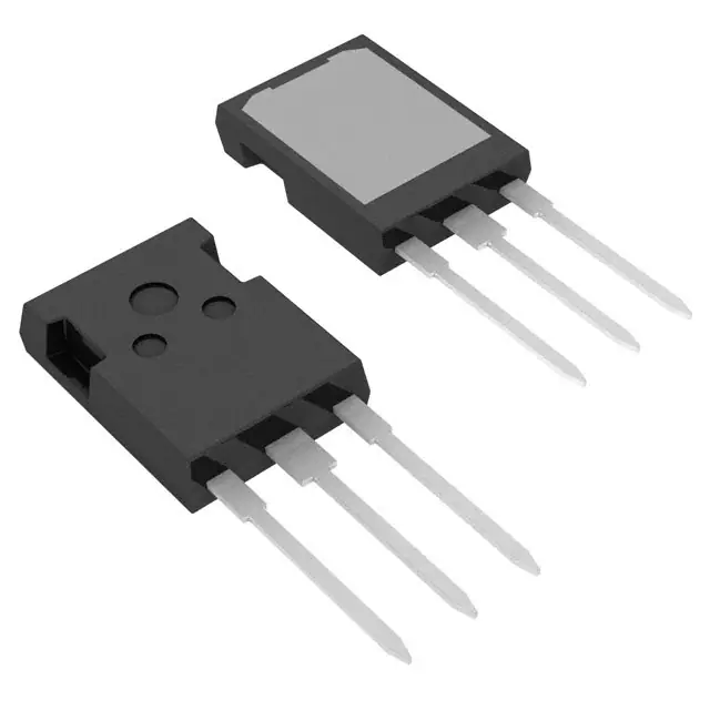
TO-264 (IXGK)
Symbol
Test Conditions
Maximum Ratings
VCES
TJ = 25°C to 150°C
300
V
VCGR
TJ = 25°C to 150°C, RGE = 1MΩ
300
V
VGES
Continuous
±20
V
VGEM
Transient
±30
V
IC25
IC110
ILRMS
ICM
TC = 25°C (Chip Capability)
TC = 110°C
Terminal Current Limit
TC = 25°C, 1ms
400
200
160
1200
A
A
A
A
SSOA
(RBSOA)
VGE = 15V, TVJ = 125°C, RG = 1Ω
Clamped Inductive Load
ICM = 400
@ 0.8 • VCES
A
PC
TC = 25°C
1000
W
TJ
TJM
-55 ... +150
150
°C
°C
Tstg
-55 ... +150
°C
300
260
°C
°C
1.13/10
20..120/4.5..27
Nm/lb.in.
N/lb.
10
6
g
g
TL
TSOLD
Maximum Lead Temperature for Soldering
1.6 mm (0.062 in.) from Case for 10
Md
FC
Mounting Torque ( IXGK )
Mounting Force ( IXGX )
Weight
TO-264
PLUS247
G
G
BVCES
IC
= 1mA, VGE = 0V
300
VGE(th)
IC
= 4mA, VCE = VGE
3.0
ICES
VCE = VCES, VGE = 0V
V
5.0
50 μA
2 mA
TJ = 125°C
IGES
VCE = 0V, VGE = ±20V
VCE(sat)
IC
IC
= 100A, VGE = 15V, Note 1
= 400A
V
±400 nA
1.15
1.70
V
V
Tab
E
Tab
E
= Emitter
Tab = Collector
Features
z
z
z
Optimized for Low Conduction Losses
High Avalanche Capability
International Standard Packages
Advantages
High Power Density
Low Gate Drive Requirement
Applications
z
z
z
z
z
z
z
z
z
© 2009 IXYS CORPORATION, All Rights Reserved
C
G = Gate
C = Collector
z
Characteristic Values
Min.
Typ.
Max.
E
E
PLUS247TM (IXGX)
z
Symbol
Test Conditions
(TJ = 25°C, Unless Otherwise Specified)
C
Power Inverters
UPS
Motor Drives
SMPS
PFC Circuits
Battery Chargers
Welding Machines
Lamp Ballasts
Inrush Current Protection Circuits
DS99584B(12/09)
�IXGK400N30A3
IXGX400N30A3
Symbol
Test Conditions
(TJ = 25°C, Unless Otherwise Specified)
Characteristic Values
Min.
Typ.
Max.
gfs
100
IC
= 60A, VCE = 10V, Note 1
170
S
19
nF
1350
pF
190
pF
Cies
Coes
VCE = 25V, VGE = 0V, f = 1 MHz
Cres
Qg(on)
Qge
IC = 100A, VGE = 15V, VCE = 0.5 • VCES
Qgc
td(on)
tr
td(off)
tf
td(on)
tr
td(off)
tf
TO-264 (IXGK) Outline
Resistive load, TJ = 25°C
IC = 100A, VGE = 15V
VCE = 240V, RG = 1Ω
Resistive load, TJ = 125°C
IC = 100A, VGE = 15V
VCE = 240V, RG = 1Ω
560
nC
83
nC
185
nC
45
ns
45
ns
210
ns
107
ns
47
ns
53
ns
240
ns
315
ns
0.125 °C/W
RthJC
RthCK
0.15
°C/W
PLUS247TM (IXGX) Outline
Note 1. Pulse test, t ≤ 300μs, duty cycle, d ≤ 2%.
Terminals: 1 - Gate
2 - Drain (Collector)
3 - Source (Emitter)
Dim.
A
A1
A2
b
b1
b2
C
D
E
e
L
L1
Q
R
IXYS Reserves the Right to Change Limits, Test Conditions, and Dimensions.
IXYS MOSFETs and IGBTs are covered
4,835,592
by one or more of the following U.S. patents: 4,850,072
4,881,106
4,931,844
5,017,508
5,034,796
5,049,961
5,063,307
5,187,117
5,237,481
5,381,025
5,486,715
6,162,665
6,259,123 B1
6,306,728 B1
6,404,065 B1
6,534,343
6,583,505
Millimeter
Min. Max.
4.83
5.21
2.29
2.54
1.91
2.16
1.14
1.40
1.91
2.13
2.92
3.12
0.61
0.80
20.80 21.34
15.75 16.13
5.45 BSC
19.81 20.32
3.81
4.32
5.59
6.20
4.32
4.83
Inches
Min. Max.
.190 .205
.090 .100
.075 .085
.045 .055
.075 .084
.115 .123
.024 .031
.819 .840
.620 .635
.215 BSC
.780 .800
.150 .170
.220 0.244
.170 .190
6,683,344
6,727,585
7,005,734 B2
6,710,405 B2 6,759,692
7,063,975 B2
6,710,463
6,771,478 B2 7,071,537
7,157,338B2
�IXGK400N30A3
IXGX400N30A3
Fig. 2. Output Characteristics @ T J = 125ºC
Fig. 1. Output Characteristics @ T J = 25ºC
300
350
VGE = 15V
11V
9V
300
250
IC - Amperes
250
IC - Amperes
VGE = 15V
11V
9V
7V
200
150
200
7V
150
100
100
5V
50
50
5V
0
0
0.0
0.2
0.4
0.6
0.8
1.0
1.2
1.4
1.6
1.8
2.0
2.2
0.0
2.4
0.2
0.4
0.6
VCE - Volts
1.0
1.2
1.4
1.8
14
15
3.2
TJ = 25ºC
VGE = 15V
2.8
1.2
I
C
= 300A
I
2.4
1.1
1.0
I
C
VCE - Volts
VCE(sat) - Normalized
1.6
Fig. 4. Collector-to-Emitter Voltage
vs. Gate-to-Emitter Voltage
Fig. 3. Dependence of VCE(sat) on
Junction Temperature
1.3
0.8
VCE - Volts
= 200A
C
= 300A
200A
100A
2.0
1.6
0.9
1.2
0.8
I
C = 100A
0.8
0.7
-50
-25
0
25
50
75
100
125
5
150
6
7
8
9
10
11
12
13
VGE - Volts
TJ - Degrees Centigrade
Fig. 5. Input Admittance
Fig. 6. Transconductance
280
350
240
300
TJ = - 40ºC
250
TJ = 125ºC
25ºC
- 40ºC
160
g f s - Siemens
IC - Amperes
200
120
25ºC
200
125ºC
150
80
100
40
50
0
0
4.0
4.4
4.8
5.2
5.6
VGE - Volts
© 2009 IXYS CORPORATION, All Rights Reserved
6.0
6.4
6.8
0
40
80
120
160
IC - Amperes
200
240
280
�IXGK400N30A3
IXGX400N30A3
Fig. 8. Capacitance
Fig. 7. Gate Charge
16
100,000
f = 1 MHz
VCE = 150V
14
I G = 10mA
12
VGE - Volts
Capacitance - PicoFarads
I C = 100A
10
8
6
4
Cies
10,000
Coes
1,000
Cres
2
100
0
0
100
200
300
400
500
0
600
5
10
15
20
25
30
35
40
VCE - Volts
QG - NanoCoulombs
Fig. 10. Maximum Transient Thermal Impedance
Fig. 9. Reverse-Bias Safe Operating Area
1.000
450
400
300
Z(th)JC - ºC / W
IC - Amperes
350
250
200
150
0.100
0.010
TJ = 125ºC
100
RG = 1Ω
dv / dt < 10V / ns
50
0
25
75
125
175
225
275
325
VCE - Volts
IXYS Reserves the Right to Change Limits, Test Conditions, and Dimensions.
0.001
0.00001
0.0001
0.001
0.01
0.1
Pulse Width - Seconds
1
10
�IXGK400N30A3
IXGX400N30A3
Fig. 11. Resistive Turn-on Rise Time
vs. Junction Temperature
Fig. 12. Resistive Turn-on Rise Time
vs. Collector Current
56
56
RG = 1Ω , VGE = 15V
I
VCE = 240V
54
= 300A, 200A, 100A
C
TJ = 125ºC
t r - Nanoseconds
t r - Nanoseconds
54
52
50
48
52
RG = 1Ω , VGE = 15V
VCE = 240V
50
48
TJ = 25ºC
46
46
44
100
44
25
35
45
55
65
75
85
95
105
115
125
120
140
160
180
Fig. 13. Resistive Turn-on Switching Times
vs. Gate Resistance
td(on) - - - -
64
80
60
70
56
60
52
50
48
40
44
30
2
3
4
5
6
7
8
9
300
220
I C = 300A, 200A, 100A
200
200
100
190
25
10
35
45
td(off) - - - -
900
VCE = 240V
800
300
700
= 100A
600
500
I C = 200A, 300A
240
400
220
300
200
200
180
100
3
4
5
6
RG - Ohms
95
105
115
180
125
7
© 2009 IXYS CORPORATION, All Rights Reserved
8
240
1000
9
10
tf
300
td(off) - - - -
230
RG = 1Ω, VGE = 15V
VCE = 240V
t f - Nanoseconds
t f - Nanoseconds
TJ = 125ºC, VGE = 15V
2
85
250
220
TJ = 125ºC
200
210
150
200
TJ = 25ºC
100
50
100
t d ( o f f ) - Nanoseconds
tf
340
1
75
350
t d ( o f f ) - Nanoseconds
360
260
65
Fig. 16. Resistive Turn-off Switching Times
vs. Collector Current
1100
C
55
TJ - Degrees Centigrade
380
I
210
150
Fig. 15. Resistive Turn-off Switching Times
vs. Gate Resistance
280
230
250
RG - Ohms
320
300
240
VCE = 240V
50
40
1
280
t d ( o f f ) - Nanoseconds
68
td(off) - - - -
RG = 1Ω, VGE = 15V
72
I C = 200A, 100A
90
tf
350
VCE = 240V
100
260
250
76
t f - Nanoseconds
110
TJ = 125ºC, VGE = 15V
240
400
t d ( o n ) - Nanoseconds
t r - Nanoseconds
80
tr
220
Fig. 14. Resistive Turn-off Switching Times
vs. Junction Temperature
130
120
200
IC - Amperes
TJ - Degrees Centigrade
190
120
140
160
180
200
220
240
260
280
180
300
IC - Amperes
IXYS REF: G_400N30A3(96)11-18-08-A
�Disclaimer Notice - Information furnished is believed to be accurate and reliable. However, users should independently
evaluate the suitability of and test each product selected for their own applications. Littelfuse products are not designed for,
and may not be used in, all applications. Read complete Disclaimer Notice at www.littelfuse.com/disclaimer-electronics.
�