IXKH 30N60C5
CoolMOS™ 1) Power MOSFET
ID25
=
30 A
VDSS
= 600 V
RDS(on) max = 0.125 Ω
N-Channel Enhancement Mode
Low RDSon, High VDSS MOSFET
Ultra low gate charge
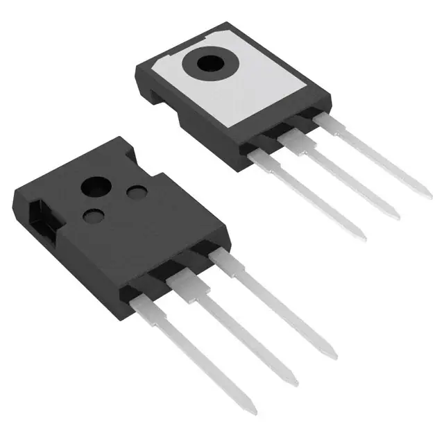
D
TO-247 AD
G
G
D
q D(TAB)
S
S
Features
MOSFET
Symbol
Conditions
VDSS
TVJ = 25°C
Maximum Ratings
VGS
ID25
ID90
TC = 25°C
TC = 90°C
EAS
EAR
single pulse
repetitive
dV/dt
MOSFET dV/dt ruggedness VDS = 0...480 V
Symbol
Conditions
ID = 11 A; TC = 25°C
600
V
± 20
V
30
21
A
A
708
1.2
mJ
mJ
50
V/ns
Characteristic Values
(TVJ = 25°C, unless otherwise specified)
min.
typ.
max.
110
125
3
3.5
V
2
µA
µA
100
nA
RDSon
VGS = 10 V; ID = 16 A
VGS(th)
VDS = VGS; ID = 1.1 mA
IDSS
VDS = 600 V; VGS = 0 V
IGSS
VGS = ± 20 V; VDS = 0 V
Ciss
Coss
VGS = 0 V; VDS = 100 V
f = 1 MHz
Qg
Qgs
Qgd
VGS = 0 to 10 V; VDS = 400 V; ID = 16 A
53
12
18
td(on)
tr
td(off)
tf
VGS = 10 V; VDS = 400 V
ID = 16 A; RG = 3.3 Ω
15
5
50
5
2.5
TVJ = 25°C
TVJ = 125°C
20
2500
120
RthJC
IXYS reserves the right to change limits, test conditions and dimensions.
© 2009 IXYS All rights reserved
mΩ
• fast CoolMOS™ 1) power MOSFET
4th generation
- High blocking capability
- Lowest resistance
- Avalanche rated for unclamped
inductive switching (UIS)
- Low thermal resistance
due to reduced chip thickness
• Enhanced total power density
Applications
• Switched mode power supplies
(SMPS)
• Uninterruptible power supplies (UPS)
• Power factor correction (PFC)
• Welding
• Inductive heating
• PDP and LCD adapter
1)
CoolMOS™ is a trademark of
Infineon Technologies AG.
pF
pF
70
nC
nC
nC
ns
ns
ns
ns
0.4
K/W
20090209d
1-4
�IXKH 30N60C5
Source-Drain Diode
Symbol
Conditions
Characteristic Values
(TVJ = 25°C, unless otherwise specified)
min.
typ.
IS
VGS = 0 V
VSD
IF = 16 A; VGS = 0 V
0.9
trr
QRM
IRM
IF = 16 A; -diF/dt = 100 A/µs; VR = 400 V
430
9
42
max.
16
A
1.2
V
ns
µC
A
Component
Symbol
Conditions
TVJ
Tstg
operating
Md
mounting torque
Symbol
Conditions
Maximum Ratings
with heatsink compound
0.8 ... 1.2
Nm
typ.
max.
0.25
K/W
6
g
Weight
IXYS reserves the right to change limits, test conditions and dimensions.
© 2009 IXYS All rights reserved
°C
°C
Characteristic Values
min.
RthCH
-55...+150
-55...+150
20090209d
2-4
�IXKH 30N60C5
TO-247 AD Outline
Symbol
A
A1
A2
D
E
E2
e
L
L1
ØP
Q
S
b
b2
b4
c
D1
D2
E1
ØP1
Inches
min
max
0.185
0.209
0.087
0.102
0.059
0.098
0.819
0.845
0.610
0.640
0.170
0.216
0.215 BSC
0.780
0.800
0.177
0.140
0.144
0.212
0.244
0.242 BSC
0.039
0.055
0.065
0.094
0.102
0.135
0.015
0.035
0.515
0.020
0.053
0.530
0.291
Millimeters
min
max
4.70
5.30
2.21
2.59
1.50
2.49
20.79
21.45
15.48
16.24
4.31
5.48
5.46 BSC
19.80
20.30
4.49
3.55
3.65
5.38
6.19
6.14 BSC
0.99
1.40
1.65
2.39
2.59
3.43
0.38
0.89
13.07
0.51
1.35
13.45
7.39
50
120
350
TJ = 125°C
TJ = 25°C
105
300
VGS =
20 V
10 V
VGS =20 V
10 V 8 V
7V
8V
40
6V
90
250
5.5 V
75
30
7V
I D [A ]
Ptot [ W]
I D [A ]
200
60
150
6V
100
5.5 V
30
4.5 V
10
5V
50
5V
20
45
15
4.5 V
0
0
0
0
40
80
120
TC [°C]
Fig. 1 Power dissipation
160
0
5
10
V
[V]
Fig. 2 Typ. output characteristics
IXYS reserves the right to change limits, test conditions and dimensions.
© 2009 IXYS All rights reserved
DS
15
20
0
5
10
15
20
V DS [V]
Fig. 3 Typ. output characteristics
20090209d
3-4
�IXKH 30N60C5
0.5
120
0.4
TJV = 150°C
0.4
20 V
VDS =
VDS > 2·RDS(on) max · ID
ID = 16 A
VGS = 10 V
6 V 6.5 V
7V
5.5 V
25 °C
0.3
5V
I D [A ]
[Ω]
DS (on)
0.2
TJ =
150 °C
R
R
DS (on)
[Ω]
80
0.3
0.2
typ
98 %
40
0.1
0.1
0
0
0
10
20
30
40
50
0
-60
-20
20
60
I D [A]
0
180
2
10
150 °C, 98%
VDS = 120 V1 20 V
TJ =150 °C
10
40 0V
Ciss
10
3
10
2
10
1
10
0
Coss
C [pF ]
[V ]
6
5
V
GS
10
4
7
I F [A ]
8
[V]
VGS = 0 V
f = 1 MHz
8
25 °C
6
GS
5
ID = 16 A pulsed
9
4
10
4
Fig. 6 Typ. transfer characteristics
10
1
2
V
Fig. 5 Drain-source on-state resistance
25 °C, 98%
10
140
T j [°C]
Fig. 4 Typ. drain-source on-state
resistance characteristics of IGBT
10
100
Crss
0
3
2
1
10
-1
0
0
0.5
1
V
SD
1.5
2
0
20
30
Q
[V]
Fig. 7 Forward characteristic
of reverse diode
Fig. 8
800
gate
40
50
60
0
50
100
[nC]
V
Typ. gate charge
DS
150
200
[V]
Fig. 9 Typ. capacitances
700
10
ID = 11 A
0
ID = 0.25 mA
0.5
B R (DS S )
[V ]
Z th J C [ K /W ]
660
600
400
620
V
E
AS
[mJ ]
10
0.2
10
-1
0.1
0.05
0.02
580
200
D = tp/T
0.01
single pulse
540
0
20
60
100
140
T j [°C]
180
10
-60
-20
20
60
100
140
180
T j [°C]
Fig. 10 Avalanche energy
Fig. 11 Drain-source breakdown voltage
IXYS reserves the right to change limits, test conditions and dimensions.
© 2009 IXYS All rights reserved
-2
10
-5
10
-4
10
-3
10
-2
10
-1
10
0
t p [s]
Fig. 12 Max. transient thermal
impedance
20090209d
4-4
�Disclaimer Notice - Information furnished is believed to be accurate and reliable. However, users should independently
evaluate the suitability of and test each product selected for their own applications. Littelfuse products are not designed for,
and may not be used in, all applications.Read complete Disclaimer Notice at www.littelfuse.com/disclaimer-electronics.
�
很抱歉,暂时无法提供与“IXKH30N60C5”相匹配的价格&库存,您可以联系我们找货
免费人工找货