High Speed IGBT
with Diode
IXSH 30N60B2D1*
IXST 30N60B2D1
VCES = 600 V
I C25
= 48 A
V CE(sat) = 2.5 V
*Obsolete Part Number
Short Circuit SOA Capability
Preliminary Data Sheet
Symbol
Test Conditions
Maximum Ratings
VCES
TJ = 25°C to 150°C
600
V
VCGR
TJ = 25°C to 150°C; RGE = 1 MΩ
600
V
VGES
Continuous
± 20
V
VGEM
Transient
± 30
V
IC25
TC = 25°C
48
A
IC110
TC = 110°C
30
A
IF(110)
28
A
90
A
ICM = 48
@ 0.8 VCES
A
10
µs
250
W
-55 ... +150
°C
TJM
150
°C
Tstg
-55 ... +150
°C
6
5
g
g
300
°C
260
°C
ICM
TC = 25°C, 1 ms
SSOA
(RBSOA)
VGE = 15 V, TJ = 125°C, RG = 10Ω
Clamped inductive load
tSC
(SCSOA)
VGE = 15 V, VCE = 360 V, TJ = 125°C
RG = 10 Ω, non repetitive
PC
TC = 25°C
TJ
Weight
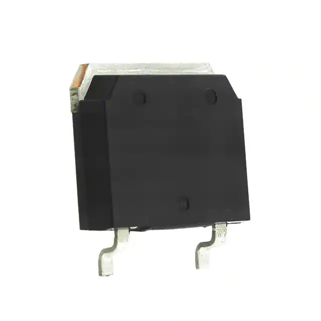
TO-247
TO-268
Maximum lead temperature for soldering
1.6 mm (0.062 in.) from case for 10 s
Maximum tab temperature for soldering for 10s
Symbol
Test Conditions
= 750 µA, VCE = VGE
VGE(th)
IC
ICES
VCE = VCES
VGE = 0 V
IGES
VCE = 0 V, VGE = ± 20 V
VCE(sat)
IC
= 24A, VGE = 15 V
G
C (TAB)
C
E
TO-268 (IXST)
G
Characteristic Values
(TJ = 25°C, unless otherwise specified)
min. typ. max.
4.0
TO-247 (IXSH)
7.0
V
150
1
µA
mA
± 100
nA
2.5
V
G = Gate
E = Emitter
E
C (TAB)
C = Collector
TAB = Collector
Features
• International standard package
• Guaranteed Short Circuit SOA
capability
• Low VCE(sat)
- for low on-state conduction losses
• High current handling capability
• MOS Gate turn-on
- drive simplicity
• Fast fall time for switching speeds
up to 20 kHz
Applications
• AC motor speed control
• Uninterruptible power supplies (UPS)
• Welding
Advantages
• High power density
DS99249(10/04)
© 2004 IXYS All rights reserved
�IXSH 30N60B2D1
IXST 30N60B2D1
Symbol
Test Conditions
Characteristic Values
(TJ = 25°C, unless otherwise specified)
min. typ.
max.
gfs
IC = 24A; VCE = 10 V, Note 1
7.0
12.0
S
1220
pF
110
140
pF
pF
C res
42
pF
Qg
50
nC
23
nC
15
nC
Cies
Coes
Qge
VCE = 25 V, VGE = 0 V
f = 1 MHz
20N60B2D1
IC = 24A, VGE = 15 V, VCE = 0.5 VCES
Qgc
td(on)
Inductive load, TJ = 25°°C
30
ns
tri
IC = 24A, VGE = 15 V
VCE = 400 V, RG = 5 Ω
Switching times may increase for VCE
(Clamp) > 0.8 • VCES, higher TJ or
increased RG
30
ns
td(off)
tfi
Eoff
td(on)
tri
Inductive load, TJ = 125°°C
Eon
IC = 24 A, VGE = 15 V
20N60B2
VCE = 400 V, RG = 5 Ω
20N60B2D1
Switching times may increase for
VCE (Clamp) > 0.8 • VCES, higher TJ
or increased RG
td(off)
tfi
Eoff
130
280
140
300
ns
0.55
1.0
mJ
30
ns
50
ns
0.32
0.82
mJ
mJ
202
ns
234
ns
1.18
mJ
RthJC
1
2
3
Terminals: 1 - Gate
Dim.
Millimeter
Min. Max.
A
4.7
5.3
A1
2.2
2.54
A2
2.2
2.6
b
1.0
1.4
b1
1.65
2.13
b2
2.87
3.12
C
.4
.8
D
20.80 21.46
E
15.75 16.26
e
5.20
5.72
L
19.81 20.32
L1
4.50
∅P 3.55
3.65
Q
5.89
6.40
0.21
Reverse Diode (FRED)
Test Conditions
K/W
Characteristic Values
(TJ = 25°C, unless otherwise specified)
min. typ. max.
VF
IF = 30A, VGE = 0 V
TJ =150°C
IRM
trr
IF = 50A, VGE = 0 V, -diF/dt = 100 A/µs
VR = 100 V
trr
IF = 1 A; -di/dt = 100 A/µs; VR = 30 V
TJ = 100°C 2.0
TJ = 100°C 150
1.6
2.5
2.5
30
V
V
A
ns
ns
0.9 K/W
RthJC
Note 1: Pulse test, t ≤ 300 µs, duty cycle d ≤ 2 %
IXYS MOSFETs and IGBTs are covered by
one or moreof the following U.S. patents:
4,835,592
4,850,072
4,881,106
4,931,844
5,017,508
5,034,796
5,049,961
5,063,307
5,187,117
5,237,481
5,381,025
5,486,715
6,162,665
6,259,123 B1
6,306,728 B1
6,404,065 B1
6,534,343
6,583,505
2 - Drain
Inches
Min. Max.
.185 .209
.087 .102
.059 .098
.040 .055
.065 .084
.113 .123
.016 .031
.819 .845
.610 .640
0.205 0.225
.780 .800
.177
.140 .144
0.232 0.252
TO-268 (IXST) Outline
0.50 K/W
RthCS
Symbol
ns
TO-247 (IXSH) Outline
6,683,344
6,710,405B2
6,710,463
6,727,585
6,759,692
�IXSH 30N60B2D1
IXST 30N60B2D1
Fig. 1. Output Characteristics
@ 25 ºC
Fig. 2. Extended Output Characteristics
@ 25 ºC
120
60
VGE = 17V
VGE = 17V
15V
100
50
13V
I C - Amperes
I C - Amperes
15V
40
30
11V
20
80
60
13V
40
11V
9V
10
20
9V
0
0
0.5
1
1.5
2
2.5
3
3.5
4
0
4.5
2
4
6
8
Fig. 3. Output Characteristics
@ 125 ºC
12
14
16
18
20
Fig. 4. Dependence of V CE(sat) on
Tem perature
60
2.0
VGE = 17V
15V
VC E (sat)- Normalized
13V
40
VGE = 15V
1.8
50
I C - Amperes
10
V C E - Volts
V C E - Volts
30
11V
20
9V
10
I C = 48A
1.6
1.4
1.2
I C = 24A
1.0
I C = 12A
0.8
7V
0
0.6
0.5
1
1.5
2
2.5
3
3.5
4
4.5
5
-50
-25
0
V CE - Volts
Fig. 5. Collector-to-Em itter Voltage
vs. Gate-to-Em itter voltage
50
75
100
125
150
Fig. 6. Input Adm ittance
110
7
TJ = 25ºC
100
6
90
80
I C = 48A
5
I C - Amperes
VC E - Volts
25
TJ - Degrees Centigrade
24A
12A
4
3
70
60
50
40
30
TJ = 125ºC
20
2
25ºC
10
1
-40ºC
0
9
10
11
12
13
14
15
V G E - Volts
16
17
18
19
6
8
10
12
V G E - Volts
14
16
18
�IXSH 30N60B2D1
IXST 30N60B2D1
Fig. 8. Dependence of Turn-off
Fig. 7. Transconductance
Energy Loss on RG
3.5
18
16
3.0
I C = 48A
E o f f - milliJoules
g f s - Siemens
14
12
10
TJ = -40ºC
8
25ºC
125ºC
6
2.5
TJ = 125ºC
VGE = 15V
2.0
VCE = 400V
I C = 24A
1.5
1.0
4
0.5
2
I C = 12A
0.0
0
0
20
40
60
80
100
0
120
10
20
30
Fig. 9. Dependence of Turn-Off
50
60
70
80
90
100
Fig. 10. Dependence of Turn-off
Energy Loss on Tem perature
Energy Loss on IC
3.0
3.0
R G = 5Ω
2.5
R G = 5Ω
TJ = 125ºC
VGE = 15V
2.5
VCE = 400V
E o f f - milliJoules
E o f f - MilliJoules
40
R G - Ohms
I C - Amperes
2.0
1.5
1.0
I C = 48A
VGE = 15V
VCE = 400V
2.0
1.5
I C = 24A
1.0
TJ = 25ºC
0.5
0.5
0.0
0.0
I C = 12A
10
15
20
25
30
35
40
45
50
25
35
I C - Amperes
45
55
65
75
85
95
Fig. 11. Dependence of Turn-off
Fig. 12. Dependence of Turn-off
Sw itching Tim e on IC
Sw itching Tim e on RG
550
260
500
tfi - - - - - -
450
TJ = 125ºC
400
VGE = 15V
I C = 12A
VCE = 400V
350
300
I C = 48A
I C = 24A
250
200
Switching Time - nanoseconds
td(off)
Switching Time - nanoseconds
105 115 125
TJ - Degrees Centigrade
td(off)
240
220
tfi - - - - - -
TJ = 125ºC
R G = 5Ω
200
VGE = 15V
180
VCE = 400V
160
140
TJ = 25ºC
120
I C = 12A
150
100
0
10
20
30
40
50
60
R G - Ohms
70
80
90
100
10
15
20
25
30
35
I C - Amperes
40
45
50
�IXSH 30N60B2D1
IXST 30N60B2D1
Fig. 13. Dependence of Turn-off
Sw itching Tim e on Tem perature
Fig. 14. Gate Charge
16
260
td(off)
Switching Time - nanoseconds
240
tfi - - - - - -
24A
12A
R G = 5Ω
220
14
I C = 48A
12
200
VG E - Volts
VGE = 15V
VCE = 400V
180
160
10
8
6
VCE = 300V
4
I C = 24A
I C = 12A
140
2
24A
48A
120
I G = 10mA
0
25
35
45
55
65
75
85
95
0
105 115 125
5
10
TJ - Degrees Centigrade
20
25
30
35
40
45
50
55
Q G - nanoCoulombs
Fig. 16. Reverse-Bias Safe
Operating Area
Fig. 15. Capacitance
10000
50
f = 1 MHz
45
40
C ies
I C - Amperes
Capacitance - p F
15
1000
C oes
100
35
30
25
20
15
10
C res
5
10
TJ = 125ºC
R G = 10Ω
dV/dT < 10V/ns
0
0
5
10
15
20
25
30
35
40
100 150 200 250 300 350 400 450 500 550 600
V C E - Volts
V C E - Volts
Fig. 17. Maxim um Transient Therm al Resistance
R ( t h ) J C - ( ºC / W )
1
0.1
1
10
100
Pulse Width - milliseconds
1000
�IXSH 30N60B2D1
IXST 30N60B2D1
60
A
1000
nC
50
IF
TVJ= 100°C
A
25
800
Qr
600
IF= 60A
IF= 30A
IF= 15A
IRM
IF= 60A
IF= 30A
IF= 15A
40
TVJ=150°C
30
TVJ= 100°C
20
30
15
TVJ=100°C
400
20
10
TVJ=25°C
200
10
0
0
1
0
100
3 V
2
5
0
A/µs 1000
-diF/dt
VF
Fig. 18. Forward current IF versus VF
Fig. 19. Reverse recovery charge
90
2.0
0
20
trr
Kf
1.00
TVJ= 100°C
µs
V
VFR
15
ns
600 A/µs
800 1000
-diF/dt
400
Fig. 20. Peak reverse current IRM
TVJ= 100°C
1.5
200
tfr
0.75
VFR
tfr
80
IF= 60A
IF= 30A
IF= 15A
1.0
IRM
10
0.50
5
0.25
70
0.5
Qr
0.0
60
0
40
80
120 °C 160
0
0
200
TVJ
400
600
800 1000
A/µs
0
400
-diF/dt
Fig.
,II
Fig.21.
20.Dynamic
Dynamicparameters
parametersQQ
r r,RM
RM
Fig. 22. Recovery time trr versus
1
K/W
0.00
600 A/µs
800 1000
diF/dt
Fig. 23. Peak forward voltage VFR
Constants for ZthJC calculation:
i
1
2
0.1
ZthJC
0.01
0.001
0.00001
200
DSEP 29-06
0.0001
0.001
0.01
s
0.1
t
Fig. 24. Transient thermal resistance junction to case
1
Rthi (K/W)
ti (s)
0.502
0.193
0.0052
0.0003
�Disclaimer Notice - Information furnished is believed to be accurate and reliable. However, users should independently
evaluate the suitability of and test each product selected for their own applications. Littelfuse products are not designed for,
and may not be used in, all applications. Read complete Disclaimer Notice at www.littelfuse.com/disclaimer-electronics.
�