High Voltage MOSFET
IXTA 2N80
IXTP 2N80
VDSS
ID25
RDS(on)
N-Channel Enhancement Mode
Avalanche Energy Rated
= 800 V
=
2 A
= 6.2 Ω
Preliminary Data
Symbol
Test Conditions
Maximum Ratings
VDSS
TJ = 25°C to 150°C
800
V
VDGR
TJ = 25°C to 150°C; RGS = 1 MΩ
800
V
VGS
Continuous
±20
V
VGSM
Transient
±30
V
ID25
TC = 25°C
2
A
IDM
TC = 25°C, pulse width limited by TJM
8
A
2
A
IAR
EAR
TC = 25°C
6
mJ
EAS
TC = 25°C
200
mJ
dv/dt
IS ≤ IDM, di/dt ≤ 100 A/µs, VDD ≤ VDSS,
TJ ≤ 150°C, RG = 18 Ω
PD
TC = 25°C
5
V/ns
54
W
-55 ... +150
°C
TJM
150
°C
Tstg
-55 ... +150
°C
TJ
Md
Mounting torque
1.13/10 Nm/lb.in.
Weight
4
Maximum lead temperature for soldering
1.6 mm (0.062 in.) from case for 10 s
g
°C
300
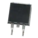
TO-220AB (IXTP)
GD
D (TAB)
S
TO-263 AA (IXTA)
G
G = Gate,
S = Source,
S
D (TAB)
D = Drain,
TAB = Drain
Features
y International standard packages
y Low RDS (on) HDMOSTM process
y Rugged polysilicon gate cell structure
y Low package inductance (< 5 nH)
- easy to drive and to protect
Symbol
Test Conditions
Characteristic Values
(TJ = 25°C, unless otherwise specified)
min. typ. max.
VDSS
VGS = 0 V, ID = 250 µA
800
VGS(th)
VDS = VGS, ID = 250 µA
2.5
IGSS
VGS = ±20 VDC, VDS = 0
IDSS
VDS = VDSS
VGS = 0 V
RDS(on)
VGS = 10 V, ID = 0.5 ID25
Pulse test, t ≤ 300 µs, duty cycle d ≤ 2 %
© 2003 IXYS All rights reserved
TJ = 125°C
V
5.5
V
y Fast switching times
Applications
y Switch-mode and resonant-mode
power supplies
±100
nA
y Flyback inverters
y DC choppers
25
500
µA
µA
Advantages
6.2
Ω
y Space savings
y High power density
98541B(01/03)
�IXTA 2N80
IXTP 2N80
Symbol
Test Conditions
Characteristic Values
(TJ = 25°C, unless otherwise specified)
min. typ. max.
gfs
VDS = 20 V; ID = 0.5 • ID25, pulse test
1.0
2.0
S
440
pF
56
pF
Crss
15
pF
td(on)
15
ns
Ciss
Coss
VGS = 0 V, VDS = 25 V, f = 1 MHz
tr
VGS = 10 V, VDS = 0.5 • VDSS, ID = 0.5 ID25
18
ns
td(off)
RG
30
ns
tf
15
ns
Qg(on)
22
nC
5.5
nC
12
nC
Qgs
= 18Ω, (External)
VGS = 10 V, VDS = 0.5 • VDSS, ID = 0.5 ID25
Qgd
RthJC
2.3
RthCK
(IXTP)
Source-Drain Diode
0.5
TO-220 AD Dimensions
Pins: 1 - Gate
3 - Source
2 - Drain
4 - Drain
Bottom Side
K/W
K/W
Characteristic Values
(TJ = 25°C, unless otherwise specified)
min. typ. max.
Symbol
Test Conditions
IS
VGS = 0 V
2
A
ISM
Repetitive; pulse width limited by TJM
8
A
VSD
IF = IS, VGS = 0 V,
Pulse test, t ≤ 300 µs, duty cycle d ≤ 2 %
1.8
V
t rr
IF
= IS, -di/dt = 100 A/µs, VR = 100 V
510
TO-263 AA Outline
ns
1.
2.
3.
4.
Gate
Drain
Source
Drain
Bottom Side
Dim.
Millimeter
Min.
Max.
Inches
Min.
Max.
A
A1
4.06
2.03
4.83
2.79
.160
.080
.190
.110
b
b2
0.51
1.14
0.99
1.40
.020
.045
.039
.055
c
c2
0.46
1.14
0.74
1.40
.018
.045
.029
.055
D
D1
8.64
7.11
9.65
8.13
.340
.280
.380
.320
E
E1
e
9.65
6.86
2.54
10.29
8.13
BSC
.380
.270
.100
.405
.320
BSC
L
L1
L2
L3
L4
14.61
2.29
1.02
1.27
0
15.88
2.79
1.40
1.78
0.38
.575
.090
.040
.050
0
.625
.110
.055
.070
.015
R
0.46
0.74
.018
.029
IXYS reserves the right to change limits, test conditions, and dimensions.
IXYS MOSFETs and IGBTs are covered by one or more of the following U.S. patents:
4,835,592
4,850,072
4,881,106
4,931,844
5,017,508
5,034,796
5,049,961
5,063,307
5,187,117
5,237,481
5,486,715
5,381,025
6,306,728B1
�Disclaimer Notice - Information furnished is believed to be accurate and reliable. However, users should independently
evaluate the suitability of and test each product selected for their own applications. Littelfuse products are not designed for,
and may not be used in, all applications. Read complete Disclaimer Notice at www.littelfuse.com/disclaimer-electronics.
�


 工商网监
湘ICP备2023018690号
工商网监
湘ICP备2023018690号
