Advance Technical Information
IXTA380N036T4-7
TrenchT4TM
Power MOSFET
VDSS
ID25
RDS(on)
= 36V
= 380A
1.0m
N-Channel Enhancement Mode
Avalanche Rated
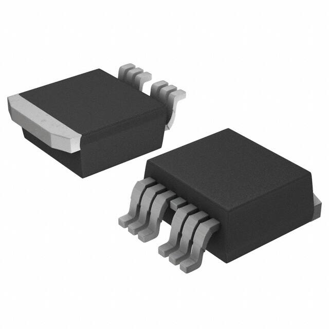
TO-263 (7-lead)
1
7
Symbol
Test Conditions
Maximum Ratings
VDSS
TJ = 25C to 175C
36
V
VDGR
TJ = 25C to 175C, RGS = 1M
36
V
VGSM
Transient
15
V
ID25
TC = 25C
380
A
ILRMS
Lead Current Limit, RMS
160
A
IDM
TC = 25C, Pulse Width Limited by TJM
830
A
IA
TC = 25C
190
A
EAS
TC = 25C
1.4
J
PD
TC = 25C
480
W
(Tab)
Pins: 1 - Gate
2, 3, 5 , 6 , 7 - Source
4 (Tab) - Drain
Features
-55 ... +175
C
TJM
175
C
Tstg
-55 ... +175
C
TJ
TL
TSOLD
Maximum Lead Temperature for Soldering
1.6 mm (0.062in.) from Case for 10s
300
260
°C
°C
FC
Mounting Force
10.65 / 2.2..14.6
N/lb
3.0
g
Weight
International Standard Package
175°C Operating Temperature
High Current Handling Capability
Avalanche Rated
Low RDS(on)
Advantages
Easy to Mount
Space Savings
High Power Density
Applications
Symbol
Test Conditions
(TJ = 25C Unless Otherwise Specified)
Characteristic Values
Min. Typ.
Max.
BVDSS
VGS = 0V, ID = 250A
36
VGS(th)
VDS = VGS, ID = 250A
2.0
IGSS
VGS = 15V, VDS = 0V
IDSS
VDS = VDSS, VGS = 0V
4.0
V
200 nA
10
TJ = 150C
RDS(on)
V
• DC-DC Converts & Off-Line UPS
• High Current Switching Applications
• Primary-Side Switch
VGS = 10V, ID = 100A, Note 1
© 2016 IXYS CORPORATION, All Rights Reserved
A
750 A
1.0 m
DS100727(5/16)
�IXTA380N036T4-7
Symbol
Test Conditions
(TJ = 25C, Unless Otherwise Specified)
Characteristic Values
Min. Typ.
Max.
gfs
VDS = 10V, ID = 60A, Note 1
105
RGi
Gate Input Resistance
175
S
1.0
13.4
nF
2400
pF
1650
pF
36
ns
78
ns
125
ns
80
ns
260
nC
60
nC
92
nC
Ciss
Coss
VGS = 0V, VDS = 25V, f = 1MHz
Crss
td(on)
tr
td(off)
tf
Resistive Switching Times
VGS = 10V, VDS = 0.5 • VDSS, ID = 0.5 • ID25
RG = 5 (External)
Qg(on)
Qgs
VGS = 10V, VDS = 0.5 • VDSS, ID = 0.5 • ID25
Qgd
RthJC
0.31C/W
Source-Drain Diode
Symbol
Test Conditions
(TJ = 25C, Unless Otherwise Specified)
Characteristic Values
Min. Typ.
Max.
IS
VGS = 0V
ISM
Repetitive, Pulse width limited by TJM
VSD
IF = 100A, VGS = 0V, Note 1
trr
IF = 150A, VGS = 0V
IRM
QRM
Note
54
-di/dt = 100A/s
VR = 30V
380
A
1520
A
1.4
V
ns
2.6
A
70
nC
1: Pulse test, t 300s, duty cycle, d 2%.
ADVANCE TECHNICAL INFORMATION
The product presented herein is under development. The Technical Specifications offered are
derived from a subjective evaluation of the design, based upon prior knowledge and experience, and constitute a "considered reflection" of the anticipated result. IXYS reserves the right
to change limits, test conditions, and dimensions without notice.
IXYS Reserves the Right to Change Limits, Test Conditions, and Dimensions.
IXYS MOSFETs and IGBTs are covered
4,835,592
by one or more of the following U.S. patents: 4,860,072
4,881,106
4,931,844
5,017,508
5,034,796
5,049,961
5,063,307
5,187,117
5,237,481
5,381,025
5,486,715
6,162,665
6,259,123 B1
6,306,728 B1
6,404,065 B1
6,534,343
6,583,505
6,683,344
6,727,585
7,005,734 B2
6,710,405 B2 6,759,692
7,063,975 B2
6,710,463
6,771,478 B2 7,071,537
7,157,338B2
�IXTA380N036T4-7
TO-263 (7-lead) (IXTA..7) Outline
A
E
OPTIONAL
c2
L2
D1
D
L
8
E1
1 2 3 4 5 6 7
L3
e
L1
c
b
A1
0- 3
Pins: 1 - Gate
2, 3, 5 , 6 , 7 - Source
4 - Drain
© 2016 IXYS CORPORATION, All Rights Reserved
IXYS REF: T_380N036T4 (T6) 5-15-16
�Disclaimer Notice - Information furnished is believed to be accurate and reliable. However, users should independently
evaluate the suitability of and test each product selected for their own applications. Littelfuse products are not designed for,
and may not be used in, all applications. Read complete Disclaimer Notice at www.littelfuse.com/disclaimer-electronics.
�