IXTH 13N110 VDSS
MegaMOSTMFET
ID25
RDS(on)
= 1100 V
= 13 A
= 0.92 Ω
N-Channel Enhancement Mode
Test Conditions
Maximum Ratings
VDSS
TJ = 25°C to 150°C
1100
V
VDGR
TJ = 25°C to 150°C; RGS = 1 MΩ
1100
V
VGS
Continuous
±20
V
VGSM
Transient
±30
V
ID25
TC = 25°C
13
A
IDM
TC = 25°C, pulse width limited by TJM
52
A
PD
TC = 25°C
360
W
-55 ... +150
°C
150
°C
-55 ... +150
°C
TJM
T stg
Md
Mounting torque
Maximum lead temperature for soldering
1.6 mm (0.062 in.) from case for 10 s
Symbol
Test Conditions
VDSS
VGS = 0 V, ID = 3 mA
VGS(th)
VDS = VGS, ID = 250 µA
IGSS
VGS = ±20 VDC, VDS = 0
IDSS
VDS = 0.8 • VDSS
VGS = 0 V
R DS(on)
6
g
300
°C
G = Gate,
S = Source,
D = Drain,
TAB = Drain
Features
l
l
l
l
Characteristic Values
(TJ = 25°C, unless otherwise specified)
min. typ. max.
1100
V
2
TJ = 25°C
TJ = 125°C
VGS = 10 V, ID = 0.5 • ID25
Pulse test, t ≤ 300 µs, duty cycle d ≤ 2 %
IXYS reserves the right to change limits, test conditions, and dimensions.
© 2000 IXYS All rights reserved
D (TAB)
1.13/10 Nm/lb.in.
OB
SO
Weight
LE
TJ
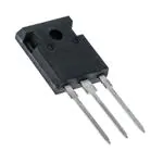
TO-247 AD
TE
Symbol
0.80
4.5
V
±100
nA
500
3
µA
mA
0.92
Ω
International standard package
JEDEC TO-247 AD
Low RDS (on) HDMOSTM process
Rugged polysilicon gate cell structure
Fast switching times
Applications
l
l
l
l
Switch-mode and resonant-mode
power supplies
Motor controls
Uninterruptible Power Supplies (UPS)
DC choppers
Advantages
l
l
l
Easy to mount with 1 screw
(isolated mounting screw hole)
Space savings
High power density
92781F (3/98)
1-2
�IXTH 13N110
Symbol
Test Conditions
Characteristic Values
(TJ = 25°C, unless otherwise specified)
min. typ. max.
gfs
VDS = 10 V; ID = 6.5 A, pulse test
C iss
C oss
VGS = 0 V, VDS = 25 V, f = 1 MHz
C rss
t d(on)
10
S
5650
pF
400
pF
150
pF
24
ns
tr
VGS = 10 V, VDS = 0.5 • VDSS, ID = 0.5 ID25
21
ns
td(off)
RG = 1 Ω, (External)
80
ns
36
ns
195
nC
28
nC
85
nC
tf
Q g(on)
Q gs
VGS = 10 V, VDS = 0.5 • VDSS, ID = 0.5 ID25
Q gd
R thJC
R thCK
0.25
Symbol
Test Conditions
IS
VGS = 0 V
ISM
Characteristic Values
(TJ = 25°C, unless otherwise specified)
min. typ. max.
A
Repetitive; pulse width limited by TJM
52
A
VSD
IF = IS, VGS = 0 V,
Pulse test, t ≤ 300 µs, duty cycle d ≤ 2 %
1.5
V
t rr
IF = IS, -di/dt = 100 A/µs, VR = 100 V
OB
SO
13
© 2000 IXYS All rights reserved
850
2
Terminals: 1 - Gate
3 - Source
K/W
K/W
LE
Source-Drain Diode
1
TE
0.35
TO-247 AD Outline
3
2 - Drain
Tab - Drain
Dim.
Millimeter
Inches
Min.
Max.
Min. Max.
A
4.7
5.3
.185 .209
A1
2.2
2.54
.087 .102
A2
2.2
2.6
.059 .098
b
1.0
1.4
.040 .055
b1
1.65
2.13
.065 .084
b2
2.87
3.12
.113 .123
C
.4
.8
.016 .031
D 20.80 21.46
.819 .845
E
15.75 16.26
.610 .640
e
5.20
5.72 0.205 0.225
L
19.81 20.32
.780 .800
L1
4.50
.177
∅ P 3.55
3.65
.140 .144
Q
5.89
6.40 0.232 0.252
R
4.32
5.49
.170 .216
S
6.15 BSC
242 BSC
ns
IXYS MOSFETS and IGBTs are covered by one or more of the following U.S. patents:
4,835,592
4,881,106
5,017,508
5,049,961
5,187,117
5,486,715
4,850,072
4,931,844
5,034,796
5,063,307
5,237,481
5,381,025
2-2
�Disclaimer Notice - Information furnished is believed to be accurate and reliable. However, users should independently
evaluate the suitability of and test each product selected for their own applications. Littelfuse products are not designed for,
and may not be used in, all applications. Read complete Disclaimer Notice at www.littelfuse.com/disclaimer-electronics.
�