Preliminary Technical Information
TrenchHVTM
Power MOSFET
IXTH160N15T
VDSS
ID25
RDS(on)
= 150
V
= 160
A
Ω
≤ 9.6 mΩ
N-Channel Enhancement Mode
Avalanche Rated
Symbol
Test Conditions
Maximum Ratings
VDSS
VDGR
TJ = 25°C to 175°C
TJ = 25°C to 175°C; RGS = 1MΩ
150
150
V
V
VGSM
Transient
± 30
V
ID25
ILRMS
IDM
TC = 25°C
Lead Current Limit, RMS
TC = 25°C, pulse width limited by TJM
160
75
430
A
A
A
IA
EAS
TC = 25°C
TC = 25°C
5
1.0
A
J
dv/dt
IS ≤ IDM, VDD ≤ VDSS, TJ ≤ 175°C
10
V/ns
Pd
TC = 25°C
830
W
-55 ... +175
175
-55 ... +175
°C
°C
°C
300
260
°C
°C
TJ
TJM
Tstg
TL
TSOLD
1.6 mm (0.062 in.) from case for 10s
Plastic body for 10 seconds
Md
Mounting torque
G
G = Gate
S = Source
D
(TAB)
S
D = Drain
TAB = Drain
1.13 / 10 Nm/lb.in.
Weight
6
Symbol
Test Conditions
(TJ = 25°C unless otherwise specified)
g
Characteristic Values
Min. Typ.
Max.
BVDSS
VGS = 0 V, ID = 250 μA
150
VGS(th)
VDS = VGS, ID = 1 mA
2.5
IGSS
VGS = ± 20 V, VDS = 0 V
IDSS
VDS = VDSS
VGS = 0 V
RDS(on)
TO-247
V
TJ = 150°C
VGS = 10 V, ID = 0.5 • ID25, Note 1
© 2007 IXYS CORPORATION, All rights reserved
8.0
5.0
V
± 200
nA
25
300
μA
μA
9.6
mΩ
Features
z
Unclamped Inductive Switching (UIS)
rated
z
Low package inductance
- easy to drive and to protect
z
175 °C Operating Temperature
Advantages
Easy to mount
z
Space savings
z
High power density
z
DS99840 (06/07)
�IXTH160N15T
Symbol
Test Conditions
Characteristic Values
(TJ = 25°C unless otherwise specified)
gfs
VDS= 10V; ID = 0.5 • ID25, Note 1
Typ.
65
105
S
8800
pF
1170
pF
150
pF
Ciss
Coss
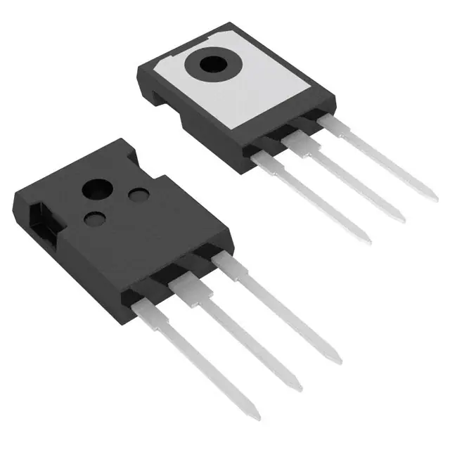
TO-247AD Outline
Min.
VGS = 0V, VDS = 25V, f = 1 MHz
Crss
Max.
td(on)
Resistive Switching Times
21
ns
tr
VGS = 15V, VDS = 0.5 • VDSS, ID = 0.5 ID25
21
ns
td(off)
RG = 2.0Ω (External)
60
ns
31
ns
160
nC
43
nC
46
nC
tf
Qg(on)
Qgs
VGS= 10V, VDS = 0.5 • VDSS, ID = 25A
Qgd
RthJC
0.18 °C/W
RthCS
0.21
°C/W
Source-Drain Diode
Symbol
Test Conditions
TJ = 25°C unless otherwise specified)
Min.
Characteristic Values
Typ.
Max.
IS
VGS = 0V
160
A
ISM
Pulse width limited by TJM
430
A
VSD
IF = 50A, VGS = 0V, Note 1
1.2
V
trr
IF = 80A, -di/dt = 200A/μs
115
1
2
3
Terminals: 1 - Gate
3 - Source
Dim.
Millimeter
Min. Max.
A
4.7
5.3
A1
2.2
2.54
A2
2.2
2.6
b
1.0
1.4
1.65
2.13
b1
b2
2.87
3.12
C
.4
.8
D
20.80 21.46
E
15.75 16.26
e
5.20
5.72
L
19.81 20.32
L1
4.50
ÆP 3.55
3.65
Q
5.89
6.40
R
4.32
5.49
S
6.15 BSC
2 - Drain
Tab - Drain
Inches
Min. Max.
.185 .209
.087 .102
.059 .098
.040 .055
.065 .084
.113 .123
.016 .031
.819 .845
.610 .640
0.205 0.225
.780 .800
.177
.140 .144
0.232 0.252
.170 .216
242 BSC
ns
VR = 75V, VGS = 0V
Notes: 1. Pulse test, t ≤ 300 ms, duty cycle, d ≤ 2 %
PRELIMINARY TECHNICAL INFORMATION
The product presented herein is under development. The Technical Specifications offered are
derived from data gathered during objective characterizations of preliminary engineering lots; but
also may yet contain some information supplied during a pre-production design evaluation. IXYS
reserves the right to change limits, test conditions, and dimensions without notice.
IXYS reserves the right to change limits, test conditions, and dimensions.
IXYS MOSFETs and IGBTs are covered
4,835,592
by one or moreof the following U.S. patents: 4,850,072
4,881,106
4,931,844
5,017,508
5,034,796
5,049,961
5,063,307
5,187,117
5,237,481
5,381,025
5,486,715
6,162,665
6,259,123 B1
6,306,728 B1
6,404,065 B1
6,534,343
6,583,505
6,683,344
6,727,585
7,005,734 B2
6,710,405 B2 6,759,692
7,063,975 B2
6,710,463
6,771,478 B2 7,071,537
7,157,338B2
�IXTH160N15T
Fig. 1. Output Characteristics
@ 25ºC
Fig. 2. Extended Output Characteristics
@ 25ºC
160
350
VGS = 10V
9V
8V
140
7V
120
250
6V
100
I D - Amperes
I D - Amperes
VGS = 10V
9V
8V
300
80
60
7V
200
150
6V
100
40
50
5V
20
5V
0
0
0
0.2
0.4
0.6
0.8
1
1.2
1.4
0
1.6
1
2
3
4
VDS - Volts
6
7
8
9
10
Fig. 4. RDS(on) Normalized to ID = 80A Value
vs. Junction Temperature
Fig. 3. Output Characteristics
@ 150ºC
160
3.0
VGS = 10V
9V
8V
7V
140
2.8
VGS = 10V
2.6
2.4
RDS(on) - Normalized
120
6V
ID - Amperes
5
VDS - Volts
100
80
60
5V
40
2.2
2.0
I D = 160A
1.8
I D = 80A
1.6
1.4
1.2
1.0
0.8
20
0.6
0
0.4
0
0.4
0.8
1.2
1.6
2
2.4
2.8
3.2
3.6
-50
-25
0
25
50
75
100
125
150
175
TJ - Degrees Centigrade
VDS - Volts
Fig. 5. RDS(on) Normalized to ID = 80A Value
vs. Drain Current
Fig. 6. Drain Current vs. Case Temperature
90
4.0
VGS = 10V
15V - - - -
3.5
External Lead Current Limit
80
I D - Amperes
RDS(on) - Normalized
70
TJ = 175ºC
3.0
2.5
2.0
60
50
40
30
1.5
TJ = 25ºC
20
1.0
10
0
0.5
0
40
80
120
160
200
I D - Amperes
© 2007 IXYS CORPORATION, All rights reserved
240
280
320
-50
-25
0
25
50
75
100
TC - Degrees Centigrade
125
150
175
�IXTH160N15T
Fig. 8. Transconductance
Fig. 7. Input Admittance
200
180
180
160
160
140
g f s - Siemens
140
ID - Amperes
TJ = - 40ºC
120
100
TJ = 150ºC
25ºC
- 40ºC
80
120
25ºC
100
150ºC
80
60
60
40
40
20
20
0
0
3.5
4
4.5
5
5.5
6
0
6.5
20
40
60
80
VGS - Volts
100
120
140
160
180
200
I D - Amperes
Fig. 9. Forward Voltage Drop of
Intrinsic Diode
Fig. 10. Gate Charge
300
10
VDS = 75V
9
250
I D = 25A
8
200
VGS - Volts
IS - Amperes
I G = 10mA
7
150
6
5
4
TJ = 150ºC
100
3
TJ = 25ºC
2
50
1
0
0
0.4
0.5
0.6
0.7
0.8
0.9
1
1.1
1.2
1.3
0
20
40
60
80
100
120
140
VSD - Volts
QG - NanoCoulombs
Fig. 11. Capacitance
Fig. 12. Maximum Transient Thermal
Impedance
100,000
160
1.00
Ciss
10,000
Z(th)JC - ºC / W
Capacitance - PicoFarads
f = 1 MHz
C oss
1,000
0.10
0.01
C rss
100
0
5
10
15
20
25
30
35
40
VDS - Volts
IXYS reserves the right to change limits, test conditions, and dimensions.
0.00
0.00001
0.0001
0.001
0.01
0.1
Pulse Width - Seconds
1
10
�IXTH160N15T
Fig. 13. Resistive Turn-on
Rise Time vs. Junction Temperature
Fig. 14. Resistive Turn-on
Rise Time vs. Drain Current
24
24
RG = 2Ω
22
VGS = 15V
TJ = 25ºC
VDS = 75V
20
t r - Nanoseconds
t r - Nanoseconds
22
18
16
I D = 40A
14
I D = 80A
12
RG = 2Ω
20
VGS = 15V
VDS = 75V
18
16
14
12
10
TJ = 125ºC
10
25
35
45
55
65
75
85
95
105
115
125
40
45
50
55
42
27
td(on) - - - -
tr
26
23
22
22
18
21
14
20
VDS = 75V
t f - Nanoseconds
24
100
RG = 2Ω, VGS = 15V
32
90
I D = 40A
28
80
I D = 80A
24
70
20
10
19
3
4
5
6
7
8
9
60
16
10
25
35
45
55
RG - Ohms
110
td(off) - - - -
t f - Nanoseconds
TJ = 125ºC
80
24
70
TJ = 25ºC
20
60
TJ = 125ºC
50
55
60
115
50
125
100
240
90
220
80
65
70
I D - Amperes
© 2007 IXYS CORPORATION, All rights reserved
75
80
200
I D = 40A
70
180
I D = 80A
60
160
50
140
40
td(off) - - - -
120
TJ = 125ºC, VGS = 15V
100
tf
30
VDS = 75V
20
16
50
105
t d ( o f f ) - Nanoseconds
90
t d ( o f f ) - Nanoseconds
VDS = 75V
32
45
95
260
100
RG = 2Ω, VGS = 15V
40
85
110
t f - Nanoseconds
tf
28
75
Fig. 18. Resistive Turn-off
Switching Times vs. Gate Resistance
40
TJ = 25ºC
65
TJ - Degrees Centigrade
Fig. 17. Resistive Turn-off
Switching Times vs. Drain Current
36
t d ( o f f ) - Nanoseconds
25
I D = 80A, 40A
2
80
td(off) - - - -
tf
36
t d ( o n ) - Nanoseconds
t r - Nanoseconds
75
110
26
VDS = 75V
30
70
40
TJ = 125ºC, VGS = 15V
34
65
Fig. 16. Resistive Turn-off
Switching Times vs. Junction Temperature
Fig. 15. Resistive Turn-on
Switching Times vs. Gate Resistance
38
60
I D - Amperes
TJ - Degrees Centigrade
80
10
60
2
3
4
5
6
7
8
9
10
RG - Ohms
IXYS REF: T_160N15T(8W) 06-07-07
�Disclaimer Notice - Information furnished is believed to be accurate and reliable. However, users should independently
evaluate the suitability of and test each product selected for their own applications. Littelfuse products are not designed for,
and may not be used in, all applications.Read complete Disclaimer Notice at www.littelfuse.com/disclaimer-electronics.
�