IXTK120P20T
IXTX120P20T
TrenchPTM
Power MOSFETs
VDSS
ID25
=
=
≤
≤
RDS(on)
trr
P-Channel Enhancement Mode
Avalanche Rated
Fast Intrinsic Rectifier
- 200V
- 120A
Ω
30mΩ
300ns
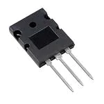
TO-264 (IXTK)
Symbol
Test Conditions
Maximum Ratings
VDSS
TJ = 25°C to 150°C
- 200
V
VDGR
TJ = 25°C to 150°C, RGS = 1MΩ
- 200
V
VGSS
Continuous
±15
V
VGSM
Transient
±25
V
ID25
TC = 25°C
-120
A
IDM
TC = 25°C, Pulse Width Limited by TJM
- 400
A
IA
EAS
TC = 25°C
TC = 25°C
-100
3
A
J
dv/dt
IS ≤ IDM, VDD ≤ VDSS, TJ ≤ 150°C
10
V/ns
PD
TC = 25°C
1040
W
-55 ... +150
150
-55 ... +150
°C
°C
°C
300
260
°C
°C
1.13/10
Nm/lb.in.
20..120 /4.5..27
N/lb.
10
6
g
g
TJ
TJM
Tstg
TL
TSOLD
Maximum Lead Temperature for Soldering
1.6 mm (0.062in.) from Case for 10s
Md
Mounting Torque (TO-264)
FC
Mounting Force
Weight
TO-264
PLUS247
(PLUS247)
G
D
S
Tab
PLUS247 (IXTX)
G
D
Tab
S
G = Gate
S = Source
D = Drain
Tab = Drain
Features
International Standard Packages
Avalanche Rated
z
Extended FBSOA
z
Fast Intrinsic Recitifier
z
Low RDS(ON) and QG
z
z
Advantages
z
z
z
Symbol
Test Conditions
(TJ = 25°C Unless Otherwise Specified)
Characteristic Values
Min.
Typ.
Max.
BVDSS
VGS = 0V, ID = - 250μA
- 200
VGS(th)
VDS = VGS, ID = - 250μA
- 2.5
V
- 4.5
V
IGSS
VGS = ±15V, VDS = 0V
±200 nA
IDSS
VDS = VDSS, VGS = 0V
- 25 μA
- 300 μA
RDS(on)
VGS = -10V, ID = 0.5 • ID25, Note 1
TJ = 125°C
© 2013 IXYS CORPORATION, All Rights Reserved
Applications
z
z
z
z
z
z
30 mΩ
Easy to Mount
Space Savings
High Power Density
High-Side Switching
Push Pull Amplifiers
DC Choppers
Automatic Test Equipment
Current Regulators
Battery Charger Applications
DS100401B(5/13)
�IXTK120P20T
IXTX120P20T
Symbol
Test Conditions
(TJ = 25°C Unless Otherwise Specified)
Characteristic Values
Min.
Typ.
Max.
gfs
85
VDS = -10V, ID = - 60A, Note 1
Ciss
Coss
VGS = 0V, VDS = - 25V, f = 1MHz
tr
td(off)
tf
S
73
nF
pF
480
pF
90
ns
Resistive Switching Times
VGS = -10V, VDS = 0.5 • VDSS, ID = 0.5 • ID25
RG = 1Ω (External)
Qg(on)
Qgs
145
2550
Crss
td(on)
TO-264 AA Outline
VGS = -10V, VDS = 0.5 • VDSS, ID = 0.5 • ID25
Qgd
85
ns
200
ns
50
ns
740
nC
220
nC
120
nC
1 - Gate
2,4 - Drain
3 - Source
0.12 °C/W
RthJC
RthCS
0.15
°C/W
Source-Drain Diode
Symbol
Test Conditions
(TJ = 25°C Unless Otherwise Specified)
Characteristic Values
Min.
Typ.
Max.
IS
VGS = 0V
-120
A
ISM
Repetitive, Pulse Width Limited by TJM
- 480
A
VSD
IF = -100A, VGS = 0V, Note 1
-1.4
V
trr
QRM
IRM
Note
IF = - 60A, -di/dt = -100A/μs
3.3
25.6
VR = -100V, VGS = 0V
PLUS247TM Outline
300 ns
μC
A
1. Pulse test, t ≤ 300μs, duty cycle, d ≤ 2%.
Terminals: 1 - Gate
2,4 - Drain
3 - Source
IXYS Reserves the Right to Change Limits, Test Conditions, and Dimensions.
IXYS MOSFETs and IGBTs are covered
4,835,592
by one or more of the following U.S. patents: 4,860,072
4,881,106
4,931,844
5,017,508
5,034,796
5,049,961
5,063,307
5,187,117
5,237,481
5,381,025
5,486,715
6,162,665
6,259,123 B1
6,306,728 B1
6,404,065 B1
6,534,343
6,583,505
6,683,344
6,727,585
7,005,734 B2
6,710,405 B2 6,759,692
7,063,975 B2
6,710,463
6,771,478 B2 7,071,537
7,157,338B2
�IXTK120P20T
IXTX120P20T
Fig. 1. Output Characteristics @ T J = 25ºC
Fig. 2. Extended Output Characteristics @ T J = 25ºC
-120
-300
VGS = -10V
- 7V
- 6V
-100
VGS = -10V
- 7V
-250
- 6V
ID - Amperes
ID - Amperes
-80
-60
- 5V
-200
-150
-40
-100
-20
-50
- 5V
- 4V
0
0
0
-0.5
-1
-1.5
-2
-2.5
0
-3
-5
-10
-20
VDS - Volts
Fig. 3. Output Characteristics @ T J = 125ºC
Fig. 4. RDS(on) Normalized to ID = - 60A Value vs.
Junction Temperature
-120
2.2
VGS = -10V
- 7V
- 6V
-100
VGS = -10V
2.0
-80
R DS(on) - Normalized
1.8
ID - Amperes
-15
VDS - Volts
- 5V
-60
-40
I D = -120A
I D = - 60A
1.6
1.4
1.2
1.0
0.8
-20
- 4V
0.6
0
0.4
0
-1
-2
-3
-4
-5
-6
-50
-25
0
VDS - Volts
Fig. 5. RDS(on) Normalized to ID = - 60A Value vs.
Drain Current
VGS = -10V
75
100
125
150
125
150
-120
TJ = 125ºC
1.8
-100
ID - Amperes
R DS(on) - Normalized
50
Fig. 6. Maximum Drain Current vs.
Case Temperature
-140
2.2
2.0
25
TJ - Degrees Centigrade
1.6
1.4
-80
-60
-40
1.2
TJ = 25ºC
-20
1.0
0
0.8
0
-40
-80
-120
-160
ID - Amperes
© 2013 IXYS CORPORATION, All Rights Reserved
-200
-240
-280
-50
-25
0
25
50
75
TC - Degrees Centigrade
100
�IXTK120P20T
IXTX120P20T
Fig. 8. Transconductance
Fig. 7. Input Admittance
-200
300
TJ = - 40ºC
-180
250
-160
g f s - Siemens
ID - Amperes
-140
-120
-100
TJ = 125ºC
25ºC
- 40ºC
-80
-60
25ºC
200
125ºC
150
100
-40
50
-20
0
-3.4
0
-3.8
-4.2
-4.6
-5
-5.4
-5.8
0
-20
-40
-60
-80
VGS - Volts
Fig. 9. Forward Voltage Drop of Intrinsic Diode
-120
-140
-160
-180
-200
-220
Fig. 10. Gate Charge
-300
-10
-9
-250
VDS = -100V
I D = - 60A
-8
I G = -1mA
-7
VGS - Volts
-200
IS - Amperes
-100
ID - Amperes
-150
TJ = 125ºC
-100
-6
-5
-4
-3
TJ = 25ºC
-2
-50
-1
0
-0.3
0
-0.4
-0.5
-0.6
-0.7
-0.8
-0.9
-1.0
-1.1
-1.2
-1.3
-1.4
0
100
200
300
VSD - Volts
500
600
700
Fig. 12. Forward-Bias Safe Operating Area
Fig. 11. Capacitance
100,000
-1,000
Ciss
f = 1 MHz
RDS(on) Limit
10,000
100µs
- 100
ID - Amperes
Capacitance - PicoFarads
400
QG - NanoCoulombs
Coss
1ms
-10
1,000
10ms
TJ = 150ºC
TC = 25ºC
Single Pulse
Crss
100ms
DC
-1
100
0
-5
-10
-15
-20
-25
-30
-35
-40
VDS - Volts
IXYS Reserves the Right to Change Limits, Test Conditions, and Dimensions.
-1
- 10
- 100
VDS - Volts
- 1,000
�IXTK120P20T
IXTX120P20T
Fig. 14. Resistive Turn-on Rise Time vs.
Drain Current
Fig. 13. Resistive Turn-on Rise Time vs.
Junction Temperature
180
180
RG = 1Ω, VGS = -10V
VDS = -100V
160
140
I
D
t r - Nanoseconds
t r - Nanoseconds
RG = 1Ω, VGS = -10V
VDS = -100V
160
= -120A
120
100
I
= - 60A
D
TJ = 125ºC
140
120
100
TJ = 25ºC
80
80
60
60
25
35
45
55
65
75
85
95
105
115
125
-60
-70
-80
TJ - Degrees Centigrade
Fig. 15. Resistive Turn-on Switching Times vs.
Gate Resistance
350
VDS = -100V
250
200
I D = -120A
300
150
I D = - 60A
200
100
100
50
0
2
3
4
5
6
7
8
9
240
60
220
55
200
I D = - 60A
I D = - 120A
50
180
45
160
40
25
10
35
45
55
65
75
85
95
105
115
RG - Ohms
TJ - Degrees Centigrade
Fig. 17. Resistive Turn-off Switching Times vs.
Drain Current
Fig. 18. Resistive Turn-off Switching Times vs.
Gate Resistance
80
td(off) - - - -
RG = 1Ω, VGS = -10V
TJ = 125ºC
60
210
55
200
50
190
TJ = 25ºC
45
180
40
-70
-80
-90
-100
ID - Amperes
© 2013 IXYS CORPORATION, All Rights Reserved
-110
170
-120
t d(off) - Nanoseconds
220
900
TJ = 125ºC, VGS = -10V
400
800
VDS = -100V
230
65
td(off) - - - -
350
700
I D = - 120A, - 60A
300
600
250
500
200
400
150
300
100
200
50
100
0
0
1
2
3
4
5
6
RG - Ohms
7
8
9
10
t d(off) - Nanoseconds
VDS = -100V
70
1000
tf
450
240
t f - Nanoseconds
tf
75
140
125
500
250
-60
td(off) - - - -
RG = 1Ω, VGS = -10V
VDS = -100V
0
1
t f - Nanoseconds
65
t d(off) - Nanoseconds
400
-120
260
tf
300
t d(on) - Nanoseconds
t r - Nanoseconds
td(on) - - - -
TJ = 125ºC, VGS = -10V
500
-110
70
t f - Nanoseconds
tr
-100
Fig. 16. Resistive Turn-off Switching Times vs.
Junction Temperature
700
600
-90
ID - Amperes
�IXTK120P20T
IXTX120P20T
Fig. 19. Maximum Transient Thermal Impedance
1
Z (th)JC - ºC / W
0.1
0.01
0.001
0.0001
0.00001
0.0001
0.001
0.01
0.1
1
10
Pulse Width - Seconds
IXYS Reserves the Right to Change Limits, Test Conditions, and Dimensions.
IXYS REF: T_120P20T(A9) 10-25-11
�Mouser Electronics
Authorized Distributor
Click to View Pricing, Inventory, Delivery & Lifecycle Information:
IXYS:
IXTX120P20T IXTK120P20T
�


 工商网监
湘ICP备2023018690号
工商网监
湘ICP备2023018690号
