IXTK 33N50
High Current
MegaMOSTMFET
VDSS = 500 V
ID (cont) = 33 A
RDS(on) = 0.17 Ω
N-Channel Enhancement Mode
Preliminary data
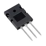
TO-264 AA
Symbol
Test conditions
VDSS
TJ = 25°C to 150°C
500
V
VDGR
TJ = 25°C to 150°C; RGS = 1.0 MΩ
500
V
VGS
Continuous
±20
V
VGSM
Transient
±30
V
ID25
T C = 25°C
IDM
PD
T
Maximum ratings
33
A
T C = 25°C, pulse width limited by TJM
132
A
T C = 25°C
416
W
J
-55 ... +150
°C
150
°C
-55 ... +150
°C
TJM
T
stg
Md
Mounting torque
Max lead temperature for soldering
1.6 mm (0.062 in.) from case for 10 s
Test Conditions
VGS = 0 V, ID = 5 mA
IDSS
VDS = 0.8 VDSS
VGS = 0 V
R DS(on)
VGS = 10 V, ID = 0.5 ID25
°C
Typ.
Max.
V
2.0
%/K
4.0
-0.25
TJ = 25°C
TJ = 125°C
IXYS reserves the right to change limits, test conditions, and dimensions.
© 2000 IXYS All rights reserved
300
0.087
VGS(th) temperature coefficient
VGS = ±20 V DC, VDS = 0
g
500
VDS = VGS, ID = 250 µA
IGSS
10
Characteristic Values
Min.
BVDSS temperature coefficient
VGS(th)
S
G = Gate
S = Source
D = Drain
TAB = Drain
Features
(T J = 25°C unless otherwise specified)
VDSS
D
1.13/10 Nm/lb.in.
Weight
Symbol
D (TAB)
G
V
%/K
±100
nA
200
3
µA
mA
0.17
Ω
• Low RDS (on) HDMOSTM process
• Rugged polysilicon gate cell
structure
• International standard package
• Fast switching times
Applications
• Motor controls
• DC choppers
• Uninterruptable Power Supplies
(UPS)
• Switch-mode and resonant-mode
Advantages
• Easy to mount with one screw
(isolated mounting screw hole)
• Space savings
• High power density
95513C (4/97)
1-4
�IXTK 33N50
Symbol
Test Conditions
(T J = 25°C unless otherwise specified)
gfs
Characteristic values
Min. Typ.
Max.
VDS = 10 V; ID = 0.5 ID25, pulse test
C iss
C oss
VGS = 0 V, VDS = 25 V, f = 1 MHz
24
S
4900
pF
690
pF
C rss
300
pF
t d(on)
53
ns
tr
VGS = 10 V, VDS = 0.5 VDSS, ID = 0.5 ID25
td(off)
RG = 1 Ω (External)
tf
30
ns
140
ns
40
ns
250
nC
30
nC
115
nC
TO-264 AA Outline
Dim.
Q g(on)
Q gs
VGS= 10 V, VDS = 0.5 VDSS, ID = 0.5 ID25
Q gd
0.30 K/W
R thJC
0.15
R thCK
Source-Drain Diode
Symbol
Test Conditions
IS
VGS= 0 V
ISM
VSD
K/W
Ratings and Characteristics
(T J = 25°C unless otherwise specified)
Min. Typ. Max.
33
A
Repetitive; pulse width limited by TJM
132
A
IF = IS, VGS = 0 V,
1.5
V
A
A1
A2
b
b1
b2
c
D
E
e
J
K
L
L1
P
Q
Q1
R
R1
S
T
Millimeter
Min.
Max.
4.82
2.54
2.00
1.12
2.39
2.90
0.53
25.91
19.81
5.46
0.00
0.00
20.32
2.29
3.17
6.07
8.38
3.81
1.78
6.04
1.57
5.13
2.89
2.10
1.42
2.69
3.09
0.83
26.16
19.96
BSC
0.25
0.25
20.83
2.59
3.66
6.27
8.69
4.32
2.29
6.30
1.83
Inches
Min.
Max.
.190
.202
.100
.114
.079
.083
.044
.056
.094
.106
.114
.122
.021
.033
1.020
1.030
.780
.786
.215 BSC
.000
.010
.000
.010
.800
.820
.090
.102
.125
.144
.239
.247
.330
.342
.150
.170
.070
.090
.238
.248
.062
.072
Pulse test, t ≤ 300 µs, duty cycle d ≤ 2 %
t rr
IF = IS, -di/dt = 100 A/µs, VR = 100 V
© 2000 IXYS All rights reserved
850
ns
IXYS MOSFETS and IGBTs are covered by one or more of the following U.S. patents:
4,835,592
4,881,106
5,017,508
5,049,961
5,187,117
5,486,715
4,850,072
4,931,844
5,034,796
5,063,307
5,237,481
5,381,025
2-4
�IXTK 33N50
50
TJ = 25°C
VGS = 10 V
9V
8V
70
ID - Amperes
50
6V
40
30
20
TJ = 125°C
VGS = 10 V
9V
8V
7V
40
7V
60
ID - Amperes
80
6V
30
20
5V
10
5V
10
0
0
0
4
8
12
16
0
20
4
8
Figure 1. Output Characteristics at 25OC
20
Figure 2. Output Characteristics at 125OC
5.5
VGS = 10 V
VGS = 10 V
5.0
RDS(ON) - Normalized
RDS(ON) - Normalized
16
VDS - Volts
VDS - Volts
3.0
2.8
2.6
2.4
2.2
2.0
1.8
1.6
1.4
1.2
1.0
0.8
12
TJ = 125°C
TJ = 25°C
4.5
ID = 33 A
4.0
3.5
3.0
2.5
ID = 16.5 A
2.0
1.5
0
10
20
30
40
50
60
70
1.0
25
80
50
ID - Amperes
75
100
125
150
TJ - Degrees C
O
Figure 4. RDS(on) normalized to 16.5A/25OC vs. TJ
Figure 3. RDS(on) normalized to 16.5A/25 C vs. ID
40
50
35
40
ID - Amperes
ID - Amperes
30
25
20
15
30
20
TJ = 125oC
10
10
5
0
-50
TJ = 25oC
-25
0
25
50
75
100 125 150
TC - Degrees C
Figure 5. Drain Current vs. Case Temperature
© 2000 IXYS All rights reserved
0
2
3
4
5
6
7
8
VGS - Volts
Figure 6. Admittance Curves
3-4
�IXTK 33N50
14
4500
Capacitance - pF
VGS - Volts
10
F=1
1MHz
MHz
4000
V
Vds=300V
ds = 300 V
= 33 A
ID=30A
= 10 mA
IG=10mA
12
8
6
4
2
Ciss
3500
3000
2500
2000
Coss
1500
1000
Crss
500
0
0
0
50
100
150
200
250
300
0
5
10
Gate Charge - nC
15
20
25
VDS - Volts
Figure 7. Gate Charge
Figure 8. Capacitance Curves
100
1 00
ID - Amperes
ID - Amperes
80
60
TJ = 125°C
40
1 ms
10
10 ms
100 ms
TC = 25°C
1
DC
20
TJ = 25°C
0
0.4
0. 1
0.6
0.8
1.0
1.2
10
1 00
VSD - Volts
500
VDS - Volts
Figure 9. Source Current vs. Source-toDrain Voltage
Figure 10. Forward Biased SOA
R(th)JC - K/W
1.00
0.10
Single Pulse
0.01
0.001
0.01
0.1
1
10
Pulse Width - Seconds
Figure 11. Transient Thermal Resistance
© 2000 IXYS All rights reserved
4-4
�Disclaimer Notice - Information furnished is believed to be accurate and reliable. However, users should independently
evaluate the suitability of and test each product selected for their own applications. Littelfuse products are not designed for,
and may not be used in, all applications. Read complete Disclaimer Notice at www.littelfuse.com/disclaimer-electronics.
�