High Voltage
Power MOSFET
VDSS
ID25
IXTL2N450
RDS(on)
(Electrically Isolated Tab)
= 4500V
= 2A
20
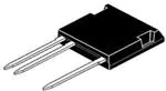
ISOPLUS i5-PakTM
N-Channel Enhancement Mode
Symbol
Test Conditions
Maximum Ratings
VDSS
TJ = 25C to 150C
4500
V
VDGR
TJ = 25C to 150C, RGS = 1M
4500
V
VGSS
Continuous
20
V
VGSM
Transient
30
V
ID25
TC = 25C
2
A
IDM
TC = 25C, Pulse Width Limited by TJM
8
A
PD
TC = 25C
220
W
- 55 ... +150
150
- 55 ... +150
C
C
C
300
260
°C
°C
20..120 / 4.5..27
N/lb.
4000
V~
8
g
TJ
TJM
Tstg
TL
TSOLD
Maximum Lead Temperature for Soldering
Plastic Body for 10s
FC
Mounting Force
VISOL
50/60Hz, 1 Minute
Weight
G
S
Isolated Tab
D
G = Gate
D = Drain
S = Source
Features
Silicon Chip on Direct-Copper Bond
(DCB) Substrate
Isolated Mounting Surface
4000V~ RMS Electrical Isolation
Molding Epoxies meet UL 94 V-0
Flammability Classification
Advantages
Symbol
Test Conditions
(TJ = 25C, Unless Otherwise Specified)
Characteristic Values
Min.
Typ. Max.
VGS(th)
VDS = VGS, ID = 250A
IGSS
VGS = 20V, VDS = 0V
200 nA
IDSS
VDS = 3.6kV, VGS = 0V
VDS = 4.5kV
VDS = 3.6kV
10 A
50 μA
μA
RDS(on)
3.5
Note 2, TJ = 125C
VGS = 10V, ID = 0.5 • ID25, Note 1
© 2013 IXYS CORPORATION, All Rights Reserved
6.0
250
20
V
Easy to Mount
Space Savings
High Power Density
Applications
High Voltage Power Supplies
Capacitor Discharge Applications
Pulse Circuits
Laser and X-Ray Generation Systems
DS100458B(9/13)
�IXTL2N450
Symbol
Test Conditions
(TJ = 25C, Unless Otherwise Specified)
Characteristic Values
Min.
Typ.
Max.
gfs
2.1
VDS = 60V, ID = 0.5 • ID25, Note 1
Ciss
Coss
3.5
S
6860
pF
VGS = 0V, VDS = 25V, f = 1MHz
Crss
RGi
td(on)
tr
td(off)
tf
Integrated Gate Input Resistance
Resistive Switching Times
pF
pF
4.0
40
ns
VGS = 10V, VDS = 1kV, ID = 1A
34
ns
123
ns
RG = 0 (External)
205
ns
180
nC
34
nC
83
nC
Qg(on)
Qgs
267
105
VGS = 10V, VDS = 1kV, ID = 0.5 • ID25
Qgd
0.56 C/W
RthJC
RthCS
C/W
0.15
Source-Drain Diode
Symbol
Test Conditions
(TJ = 25C, Unless Otherwise Specified)
Characteristic Values
Min.
Typ.
Max.
IS
VGS = 0V
2
A
ISM
Repetitive, Pulse Width Limited by TJM
8
A
VSD
IF = IS, VGS = 0V, Note 1
3
V
trr
IF = 2A, -di/dt = 100A/μs, VR = 100V
Notes:
1.75
μs
1. Pulse test, t 300s, duty cycle, d 2%.
2. Part must be heatsunk for high-temp Idss measurement.
ISOPLUS i5-PakTM (IXTL) Outline
E
Q
A
S
A2
U
R
T
Q1
D
R1
4
1
2
3
L1
1 = Gate
2 = Source
3 = Drain
4 = Isolated
L
c
b1
b2
e1
e
IXYS Reserves the Right to Change Limits, Test Conditions, and Dimensions.
IXYS MOSFETs and IGBTs are covered
4,835,592
by one or moreof the following U.S. patents: 4,860,072
4,881,106
4,931,844
5,017,508
5,034,796
5,049,961
5,063,307
5,187,117
5,237,481
5,381,025
5,486,715
6,162,665
6,259,123 B1
6,306,728 B1
6,404,065 B1
6,534,343
6,583,505
6,683,344
6,727,585
7,005,734 B2
6,710,405 B2 6,759,692
7,063,975 B2
6,710,463
6,771,478 B2 7,071,537
7,157,338B2
�IXTL2N450
Fig. 2. Output Characteristics @ TJ = 125ºC
Fig. 1. Output Characteristics @ TJ = 25ºC
1.8
3.0
VGS = 10V
VGS = 10V
1.6
6V
7V
2.5
2.0
1.2
1.5
I D - Amperes
I D - Amperes
1.4
6.5V
1.0
0.8
5.5V
0.6
1.0
0.4
0.5
6V
5V
0.2
0.0
0.0
0
10
20
30
40
50
60
70
0
10
20
30
40
50
60
VDS - Volts
VDS - Volts
Fig. 3. RDS(on) Normalized to ID = 1A Value
vs. Junction Temperature
Fig. 4. RDS(on) Normalized to ID = 1A Value
vs. Drain Current
70
2.4
2.4
VGS = 10V
2.2
VGS = 10V
2.2
RDS(on) - Normalized
RDS(on) - Normalized
2.0
I D = 2A
1.8
I D = 1A
1.6
1.4
1.2
1.0
2.0
TJ = 125ºC
1.8
1.6
1.4
1.2
0.8
TJ = 25ºC
1.0
0.6
0.4
0.8
-50
-25
0
25
50
75
100
125
150
0
0.5
1
1.5
2
2.5
3
I D - Amperes
TJ - Degrees Centigrade
Fig. 5. Maximum Drain Current vs. Case Temperature
Fig. 6. Input Admittance
1.8
2.0
1.6
1.4
1.6
I D - Amperes
I D - Amperes
1.2
1.2
0.8
1.0
0.8
TJ = 125ºC
0.6
25ºC
0.4
0.4
- 40ºC
0.2
0.0
0.0
-50
-25
0
25
50
75
TC - Degrees Centigrade
© 2013 IXYS CORPORATION, All Rights Reserved
100
125
150
4.0
4.5
5.0
5.5
VGS - Volts
6.0
6.5
7.0
�IXTL2N450
Fig. 7. Transconductance
Fig. 8. Forward Voltage Drop of Intrinsic Diode
6
6
TJ = - 40ºC
5
5
4
4
I S - Amperes
g f s - Siemens
25ºC
125ºC
3
TJ = 125ºC
3
TJ = 25ºC
2
2
1
1
0
0
0.0
0.2
0.4
0.6
0.8
1.0
1.2
1.4
1.6
1.8
0.2
0.3
0.4
0.5
0.6
I D - Amperes
0.8
0.9
1.0
30
35
40
Fig. 10. Capacitance
Fig. 9. Gate Charge
10,000
10
VDS = 1000V
9
Ciss
Capacitance - PicoFarads
I D = 1A
8
I G = 10mA
7
VGS - Volts
0.7
VSD - Volts
6
5
4
3
1,000
Coss
100
Crss
2
f = 1 MHz
1
10
0
0
20
40
60
80
100
120
140
160
0
180
5
10
15
20
25
VDS - Volts
QG - NanoCoulombs
Fig. 12. Resistive Switching Times vs.
External Gate Resistance
Fig. 11. Forward-Bias Safe Operating Area
300
10
RDS(on) Limit
VDS = 1kV, VGS = 10V
Switching Times - Nanoseconds
25µs
100µs
- Amperes
1
1ms
I
D
10ms
0.1
TJ = 150ºC
100ms
TC = 25ºC
Single Pulse
DC
ID = 1A, TJ = 25ºC
250
200
tf
150
tr
t d(off)
100
t d(on)
50
1s
0.01
0
100
1,000
10,000
VDS - Volts
IXYS Reserves the Right to Change Limits, Test Conditions, and Dimensions.
0
1
2
3
4
5
6
RG(ext) - Ohms
7
8
9
10
�IXTL2N450
Fig. 13. Maximum Transient Thermal Impedance
Z(th)JC - ºC / W
1
0.1
0.01
0.0001
0.001
0.01
0.1
1
10
100
Pulse Width - Seconds
© 2013 IXYS CORPORATION, All Rights Reserved
IXYS REF: T_2N450(H9-P640) 9-24-13
�Disclaimer Notice - Information furnished is believed to be accurate and reliable. However, users should independently
evaluate the suitability of and test each product selected for their own applications. Littelfuse products are not designed for,
and may not be used in, all applications. Read complete Disclaimer Notice at www.littelfuse.com/disclaimer-electronics.
�