Advance Technical Information
Linear L2TM Power
MOSFET w/Extended
FBSOA
IXTN110N20L2
VDSS
ID25
= 200V
= 100A
≤ 24mΩ
Ω
RDS(on)
N-Channel Enhancement Mode
Guaranteed FBSOA
Avalanche Rated
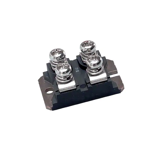
miniBLOC, SOT-227
E153432
S
Symbol
Test Conditions
Maximum Ratings
VDSS
TJ = 25°C to 150°C
200
V
VDGR
TJ = 25°C to 150°C, RGS = 1MΩ
200
V
VGSS
Continuous
±20
V
VGSM
Transient
±30
V
G
S
D
ID25
TC = 25°C
100
A
IDM
TC = 25°C, Pulse Width Limited by TJM
275
A
IA
EAS
TC = 25°C
TC = 25°C
55
5
A
J
PD
TC = 25°C
735
W
Either Source Terminal S can be used as
the Source Terminal or the Kelvin Source
(Gate Return) Terminal.
-55 ... +150
150
-55 ... +150
°C
°C
°C
Features
300
260
°C
°C
2500
3000
V~
V~
1.5/13
1.3/11.5
Nm/lb.in.
Nm/lb.in.
30
g
TJ
TJM
Tstg
TL
TSOLD
1.6mm (0.062 in.) from Case for 10s
Plastic Body for 10s
VISOL
50/60 Hz, RMS
IISOL ≤ 1mA
Md
Mounting Torque
Terminal Connection Torque
t = 1 Minute
t = 1 Second
Weight
G = Gate
S = Source
D = Drain
• Designed for Linear Operation
• International Standard Package
Guaranteed FBSOA at 75°C
• Avalanche Rated
• Molding Epoxy Meets UL94 V-0
Flammability Classification
• MiniBLOC with Aluminium Nitride
Isolation
Applications
Symbol
Test Conditions
(TJ = 25°C, Unless Otherwise Specified)
Characteristic Values
Min.
Typ.
Max.
BVDSS
VGS = 0V, ID = 1mA
200
VGS(th)
VDS = VGS, ID = 3mA
2.0
IGSS
VGS = ±20V, VDS = 0V
±200 nA
IDSS
VDS = VDSS, VGS = 0V
50 μA
2.5 mA
RDS(on)
VGS = 10V, ID = 55A, Note 1
TJ = 125°C
© 2009 IXYS CORPORATION, All Rights Reserved
V
4.5
V
•
•
•
•
•
•
Programmable Loads
Current Regulators
DC-DC Converters
Battery Chargers
DC Choppers
Temperature and Lighting Controls
Advantages
• Easy to Mount
• Space Savings
• High Power Density
24 mΩ
DS100196(9/09)
�IXTN110N20L2
Symbol
Test Conditions
(TJ = 25°C, Unless Otherwise Specified)
Characteristic Values
Min.
Typ.
Max.
gfs
55
VDS= 10V, ID = 55A, Note 1
75
Ciss
Coss
VGS = 0V, VDS = 25V, f = 1MHz
Crss
td(on)
Resistive Switching Times
tr
VGS = 10V, VDS = 0.5 • VDSS, ID = 55A
RG = 1Ω (External)
td(off)
tf
Qg(on)
Qgs
VGS= 10V, VDS = 0.5 • VDSS, ID = 55A
Qgd
SOT-227B (IXTN) Outline
95
S
23
nF
2160
pF
320
pF
40
ns
100
ns
33
ns
135
ns
500
nC
110
nC
182
nC
RthJC
(M4 screws (4x) supplied)
0.17 °C/W
RthCS
0.05
°C/W
Safe-Operating-Area Specification
Symbol
Test Conditions
Characteristic Values
Min.
Typ.
Max.
SOA
VDS = 200V, ID = 1.75A, TC = 75°C , Tp = 3s
350
W
Source-Drain Diode
Symbol
Test Conditions
(TJ = 25°C, Unless Otherwise Specified)
Characteristic Values
Min.
Typ.
Max.
IS
VGS = 0V
110
A
ISM
Repetitive, Pulse Width Limited by TJM
440
A
VSD
IF = 55A, VGS = 0V, Note 1
1.35
V
trr
IRM
QRM
IF = 55A, -di/dt = 100A/μs,
VR = 100V, VGS = 0V
Note
420
39
8.3
ns
A
μC
1. Pulse Test, t ≤ 300μs; Duty Cycle, d ≤ 2%.
ADVANCE TECHNICAL INFORMATION
The product presented herein is under development. The Technical Specifications offered are derived
from a subjective evaluation of the design, based upon prior knowledge and experience, and constitute a
"considered reflection" of the anticipated result. IXYS reserves the right to change limits, test
conditions, and dimensions without notice.
IXYS Reserves the Right to Change Limits, Test Conditions, and Dimensions.
IXYS MOSFETs and IGBTs are covered
4,835,592
by one or more of the following U.S. patents: 4,850,072
4,881,106
4,931,844
5,017,508
5,034,796
5,049,961
5,063,307
5,187,117
5,237,481
5,381,025
5,486,715
6,162,665
6,259,123 B1
6,306,728 B1
6,404,065 B1
6,534,343
6,583,505
6,683,344
6,710,405 B2
6,710,463
6,727,585
7,005,734 B2
6,759,692
7,063,975 B2
6,771,478 B2 7,071,537
7,157,338B2
�IXTN110N20L2
Fig. 2. Extended Output Characteristics
Fig. 1. Output Characteristics
@ T J = 25ºC
120
VGS = 20V
14V
12V
10V
8V
VGS = 20V
14V
12V
10V
240
200
80
8V
6.5V
ID - Amperes
ID - Amperes
100
@ T J = 25ºC
280
6V
60
160
6.5V
120
40
80
6V
5V
20
40
5V
4V
0
4V
0
0.0
0.5
1.0
1.5
2.0
2.5
3.0
0
2
4
6
8
VDS - Volts
Fig. 3. Output Characteristics
16
18
20
VGS = 10V
2.8
R DS(on) - Normalized
8V
80
ID - Amperes
14
3.2
VGS = 20V
12V
10V
100
12
Fig. 4. RDS(on) Normalized to ID = 55A Value vs.
Junction Temperature
@ T J = 125ºC
120
10
VDS - Volts
6V
60
40
5V
2.4
I D = 110A
2.0
I D = 55A
1.6
1.2
20
0.8
4V
0.4
0
0
1
2
3
4
5
6
-50
7
-25
0
Fig. 5. RDS(on) Normalized to ID = 55A Value vs.
Drain Current
50
75
100
125
150
125
150
Fig. 6. Maximum Drain Current vs.
Case Temperature
120
4.0
VGS = 10V
3.5
100
TJ = 125ºC
3.0
ID - Amperes
R DS(on) - Normalized
25
TJ - Degrees Centigrade
VDS - Volts
2.5
2.0
80
60
40
1.5
TJ = 25ºC
20
1.0
0.5
0
0
20
40
60
80
100
120
140
160
180
ID - Amperes
© 2009 IXYS CORPORATION, All Rights Reserved
200
220
240
260
-50
-25
0
25
50
75
TC - Degrees Centigrade
100
�IXTN110N20L2
Fig. 7. Input Admittance
Fig. 8. Transconductance
160
140
140
TJ = - 40ºC
120
g f s - Siemens
ID - Amperes
120
100
80
TJ = 125ºC
25ºC
- 40ºC
60
100
25ºC
80
125ºC
60
40
40
20
20
0
0
3.5
4.0
4.5
5.0
5.5
6.0
6.5
7.0
0
20
40
60
VGS - Volts
80
100
120
140
160
600
700
800
ID - Amperes
Fig. 9. Forward Voltage Drop of
Intrinsic Diode
Fig. 10. Gate Charge
320
16
280
14
240
12
200
10
VGS - Volts
IS - Amperes
VDS = 100V
160
120
TJ = 125ºC
80
I D = 55A
I G = 10mA
8
6
4
TJ = 25ºC
40
2
0
0
0.3
0.4
0.5
0.6
0.7
0.8
0.9
1.0
1.1
1.2
1.3
1.4
1.5
0
100
VSD - Volts
200
300
400
500
QG - NanoCoulombs
Fig. 12. Maximum Transient Thermal Impedance
Fig. 11. Capacitance
100,000
1.000
Ciss
10,000
Z(th)JC - ºC / W
Capacitance - PicoFarads
f = 1 MHz
Coss
1,000
0.100
0.010
Crss
100
0
5
10
15
20
25
30
35
40
VDS - Volts
IXYS Reserves the Right to Change Limits, Test Conditions, and Dimensions.
0.001
0.00001
0.0001
0.001
0.01
0.1
Pulse Width - Seconds
1
10
�IXTN110N20L2
Fig. 13. Forward-Bias Safe Operating Area
Fig. 14. Forward-Bias Safe Operating Area
@ T C = 25ºC
@ T C = 75ºC
1,000
1,000
RDS(on) Limit
RDS(on) Limit
25µs
100
25µs
100
ID - Amperes
ID - Amperes
100µs
1ms
100µs
1ms
10ms
10
10
10ms
TJ = 150ºC
100ms
TJ = 150ºC
TC = 25ºC
Single Pulse
DC
TC = 75ºC
Single Pulse
100ms
DC
DC
1
1
1
10
100
VDS - Volts
© 2009 IXYS CORPORATION, All Rights Reserved
1,000
1
10
100
1,000
VDS - Volts
IXYS REF: T_110N20L2(9R)9-16-09
�Disclaimer Notice - Information furnished is believed to be accurate and reliable. However, users should independently
evaluate the suitability of and test each product selected for their own applications. Littelfuse products are not designed for,
and may not be used in, all applications. Read complete Disclaimer Notice at www.littelfuse.com/disclaimer-electronics.
�