IXTK 120N25
High Current
MegaMOSTMFET
VDSS
ID25
= 250 V
= 120 A
Ω
= 20 mΩ
RDS(on)
N-Channel Enhancement Mode
Preliminary Data Sheet
Symbol
Test conditions
Maximum ratings
VDSS
TJ = 25°C to 150°C
250
V
VDGR
TJ = 25°C to 150°C; RGS = 1.0 MΩ
250
V
VGS
Continuous
±20
V
VGSM
Transient
±30
V
ID25
ID(RMS)
IDM
IAR
TC = 25°C MOSFET chip capability
External lead current limit
TC = 25°C, pulse width limited by TJM
TC = 25°C
120
75
480
90
A
A
A
A
EAR
EAS
TC = 25°C
TC = 25°C
80
4.0
mJ
J
dv/dt
IS ≤ IDM, di/dt ≤ 100 A/µs, VDD ≤ VDSS
TJ ≤ 150°C, RG = 2 Ω
10
V/ns
PD
TC
730
W
TJ
-55 ... +150
°C
TJM
Tstg
150
-55 ... +150
°C
°C
300
°C
= 25°C
TL
1.6 mm (0.063 in.) from case for 10 s
Md
Mounting torque
Weight
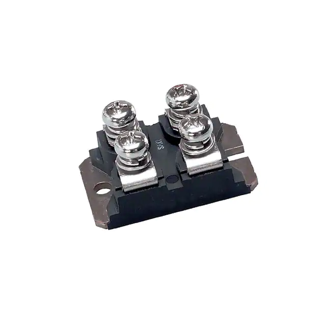
TO-264
0.7/6
Nm/lb.in.
10
g
TO-264 AA (IXTK)
G
D (TAB)
D
S
G = Gate
S = Source
D
= Drain
Tab = Drain
Features
•Low RDS (on) HDMOSTM process
•Rugged polysilicon gate cell structure
•International standard package
•Fast switching times
Applications
Symbol Test Conditions
(TJ = 25°C unless otherwise specified)
Characteristic Values
Min. Typ.
Max.
VDSS
V GS = 0 V, ID = 1 mA
VGS(th)
V DS = VGS, ID = 250 µA
IGSS
V GS = ±20 V DC, VDS = 0
IDSS
V DS = VDSS
V GS = 0 V
RDS(on)
VGS = 10 V, ID = 0.5 ID25
Pulse test, t ≤ 300 ms, duty cycle d ≤ 2%
© 2003 IXYS All rights reserved
250
2.0
TJ = 25°C
TJ = 125°C
V
4.0
V
±200
nA
50 µA
3 mA
• Motor controls
• DC choppers
• Switched-mode power supplies
Advantages
• Easy to mount with one screw
(isolated mounting screw hole)
• Space savings
• High power density
20 mΩ
DS98879D(11/03)
�IXTK 120N25
Symbol
Test Conditions
(T J = 25°C unless otherwise specified)
gfs
Characteristic values
Min. Typ.
Max.
VDS = 10 V; ID = 0.5 ID25, pulse test
65
Ciss
S
7700
pF
1700
pF
C rss
600
pF
td(on)
35
ns
Coss
VGS = 0 V, VDS = 25 V, f = 1 MHz
98
tr
VGS = 10 V, VDS = 0.5 VDSS, ID = 0.5 ID25
td(off)
RG = 1.5 Ω (External)
tf
ns
ns
35
ns
360
Qg(on)
Qgs
38
175
VGS = 10 V, VDS = 0.5 VDSS, ID = 0.5 ID25
Qgd
nC
63
nC
180
nC
0.17 K/W
RthJC
RthCK
0.15
Source-Drain Diode
K/W
TO-264 AA Outline
Dim.
A
A1
A2
b
b1
b2
c
D
E
e
J
K
L
L1
P
Q
Q1
R
R1
S
T
Millimeter
Min.
Max.
4.82
5.13
2.54
2.89
2.00
2.10
1.12
1.42
2.39
2.69
2.90
3.09
0.53
0.83
25.91
26.16
19.81
19.96
5.46 BSC
0.00
0.25
0.00
0.25
20.32
20.83
2.29
2.59
3.17
3.66
6.07
6.27
8.38
8.69
3.81
4.32
1.78
2.29
6.04
6.30
1.57
1.83
Ratings and Characteristics
(TJ = 25°C unless otherwise specified)
Min.
Typ.
Max.
Symbol
Test Conditions
IS
VGS = 0V
120
A
ISM
Repetitive; pulse width limited by TJM
480
A
VSD
IF = IS, VGS = 0 V,
Pulse test, t ≤ 300 µs, duty cycle d ≤ 2 %
1.5
V
t rr
IF = 25A, -di/dt = 100 A/µs, VR = 100V
Qrr
IXYS MOSFETS and IGBTs are covered by one or more of the
4,835,592
4,881,106
5,017,508
4,850,072
4,931,844
5,034,796
IXYS reserves the right to change limits, test conditions,
350
ns
4
µC
following U.S. patents:
5,049,961
5,187,117
5,063,307
5,237,481
and dimensions.
5,486,715
5,381,025
6,306,728B1
Min.
Inches
Max.
.190
.202
.100
.114
.079
.083
.044
.056
.094
.106
.114
.122
.021
.033
1.020
1.030
.780
.786
.215 BSC
.000
.010
.000
.010
.800
.820
.090
.102
.125
.144
.239
.247
.330
.342
.150
.170
.070
.090
.238
.248
.062
.072
�IXTK 120N25
Fig. 1. Output Characteristics
@ 25 Deg. C
Fig. 2. Extended Output Characteristics
@ 25 deg. C
220
120
VGS = 10V
7V
6V
110
100
180
160
80
I D - Amperes
I D - Amperes
90
VGS = 10V
8V
7V
200
70
60
50
40
5V
120
100
80
60
30
20
40
10
20
0
0
0
0.5
1
6V
140
1.5
2
5V
0
2.5
1
2
3
Fig. 3. Output Characteristics
@ 125 Deg. C
6
7
8
9
10
Fig. 4. RDS(on) Norm alized to ID25 Value vs.
Junction Tem perature
VGS = 10V
7V
6V
110
100
2.4
R D S (on) - Normalized
80
70
60
VGS = 10V
2.2
90
I D - Amperes
5
2.6
120
5V
50
40
30
2
1.8
I D = 120A
1.6
1.4
I D = 60A
1.2
1
20
0.8
10
0.6
0
0.4
0
1
2
3
4
5
-50
-25
V D S - Volts
0
25
50
75
100
125
150
TJ - Degrees Centigrade
Fig. 5. RDS(on) Norm alized to ID25
Value vs. ID
Fig. 6. Drain Current vs. Case
Tem perature
130
2.4
120
VGS = 10V
2.2
110
TJ = 125ºC
2
100
90
I D - Amperes
R D S (on) - Normalized
4
V D S - Volts
V D S - Volts
1.8
1.6
1.4
80
70
60
50
40
1.2
TJ = 25ºC
30
20
1
10
0.8
0
0
20
40
60
80 100 120 140 160 180 200 220
I D - Amperes
© 2003 IXYS All rights reserved
-50
-25
0
25
50
75
100
TC - Degrees Centigrade
125
150
�IXTK 120N25
Fig. 8. Transconductance
Fig. 7. Input Adm ittance
140
200
180
120
TJ = -40ºC
25ºC
125ºC
100
140
g f s - Siemens
I D - Amperes
160
120
100
80
60
80
60
40
TJ = 125ºC
25ºC
-40ºC
40
20
20
0
0
3
3.5
4
4.5
5
5.5
6
6.5
0
20
40
60
V G S - Volts
200
10
180
9
160
8
140
7
120
100
TJ = 125ºC
60
100 120 140 160 180 200
Fig. 10. Gate Charge
VG S - Volts
I S - Amperes
Fig. 9. Source Current vs. Source-ToDrain Voltage
80
80
I D - Amperes
VDS = 125V
I D = 60A
I G = 10mA
6
5
4
3
40
2
TJ = 25ºC
20
1
0
0
0.4
0.6
0.8
1
1.2
1.4
0
50
100
150
200
250
300
350
Q G - nanoCoulombs
V S D - Volts
Fig. 12. Forw ard Bias Safe
Operating Area
Fig. 11. Capacitance
10000
1000
TC = 25ºC
R DS(on) Limit
I D - Amperes
Capacitance - pF
C iss
C oss
1000
25µs
100
1ms
DC
10
C rss
f = 1MHz
100
1
0
5
10
15
20
25
V D S - Volts
30
35
40
IXYS reserves the right to change limits, test conditions, and dimensions.
1
10
100
V D S - Volts
1000
�IXTK 120N25
Fig . 13. M axim u m T r an s ie n t T h e r m al Re s is tan ce
0.18
0.16
R (th) J C - (ºC/W)
0.14
0.12
0.10
0.08
0.06
0.04
0.02
0.00
1
10
100
Puls e W idth - millis ec onds
© 2003 IXYS All rights reserved
10 0 0
�Mouser Electronics
Authorized Distributor
Click to View Pricing, Inventory, Delivery & Lifecycle Information:
IXYS:
IXTN120N25
�