Preliminary Technical Information
IXTN210P10T
TrenchPTM
Power MOSFET
VDSS
ID25
RDS(on)
D
P-Channel Enhancement Mode
Avalanche Rated
Fast Intrinsic Rectifier
trr
=
=
≤
≤
-100V
- 210A
Ω
7.5mΩ
200ns
G
S
miniBLOC
E153432
S
S
G
Symbol
Test Conditions
Maximum Ratings
VDSS
TJ = 25°C to 150°C
-100
VDGR
TJ = 25°C to 150°C, RGS = 1MΩ
-100
V
VGSS
Continuous
±15
V
VGSM
Transient
±25
V
ID25
TC = 25°C (Chip Capability)
- 210
A
ILRMS
Lead Current Limit, RMS
- 200
A
IDM
TC = 25°C, Pulse Width Limited by TJM
- 800
A
IA
EAS
TC = 25°C
TC = 25°C
-100
3
A
J
dv/dt
IS ≤ IDM, VDD ≤ VDSS, TJ ≤ 150°C
10
V/ns
PD
TC = 25°C
830
W
- 55 ... +150
150
- 55 ... +150
°C
°C
°C
2500
3000
V~
V~
1.5/13
1.3/11.5
Nm/lb.in.
Nm/lb.in.
30
g
TJ
TJM
Tstg
VISOL
50/60 Hz, RMS, t = 1minute
IISOL ≤ 1mA,
t = 1s
Md
Mounting Torque for Base Plate
Terminal Connection Torque
S
V
D
G = Gate
S = Source
Either Source Terminal S can be used as
the Source Terminal or the Kelvin Source
(Gate Return) Terminal.
Features
International Standard Package
Low Intrinsic Gate Resistance
z
miniBLOC with Aluminum Nitride
Isolation
z
Avalanche Rated
z
Extended FBSOA
z
Fast Intrinsic Recitifier
z
Low RDS(ON) and QG
z
Weight
z
Advantages
z
z
z
Symbol
Test Conditions
(TJ = 25°C, Unless Otherwise Specified)
Characteristic Values
Min.
Typ.
Max.
BVDSS
VGS = 0V, ID = - 250μA
-100
VGS(th)
VDS = VGS, ID = - 250μA
- 2.5
IGSS
VGS = ±15V, VDS = 0V
±200 nA
IDSS
VDS = VDSS, VGS = 0V
- 25 μA
- 300 μA
RDS(on)
V
- 4.5
V
VGS = -10V, ID = 0.5 • ID25, Note 1
© 2011 IXYS CORPORATION, All Rights Reserved
Easy to Mount
Space Savings
High Power Density
Applications
z
z
z
z
TJ = 125°C
D = Drain
z
z
High-Side Switching
Push Pull Amplifiers
DC Choppers
Automatic Test Equipment
Current Regulators
Battery Charger Applications
7.5 mΩ
DS100408A(01/13)
�IXTN210P10T
Symbol
Test Conditions
(TJ = 25°C, Unless Otherwise Specified)
gfs
Characteristic Values
Min.
Typ.
Max.
VDS = -10V, ID = - 60A, Note 1
90
Ciss
Coss
VGS = 0V, VDS = - 25V, f = 1MHz
Crss
td(on)
tr
td(off)
tf
RG = 1Ω (External)
Qg(on)
Qgs
150
S
69.5
nF
4070
pF
1100
pF
90
ns
98
ns
165
ns
55
ns
740
nC
200
nC
155
nC
Resistive Switching Times
VGS = -10V, VDS = 0.5 • VDSS, ID = 0.5 • ID25
VGS = -10V, VDS = 0.5 • VDSS, ID = 0.5 • ID25
Qgd
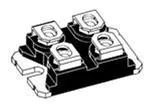
SOT-227B (IXTN) Outline
(M4 screws (4x) supplied)
0.15 °C/W
RthJC
RthCS
0.05
°C/W
Source-Drain Diode
Symbol
Test Conditions
(TJ = 25°C, Unless Otherwise Specified)
Characteristic Values
Min.
Typ.
Max.
IS
VGS = 0V
- 210
A
ISM
Repetitive, Pulse Width Limited by TJM
- 840
A
VSD
IF = -100A, VGS = 0V, Note 1
-1.4
V
trr
QRM
IRM
IF = -105A, -di/dt = -100A/μs
VR = -100V, VGS = 0V
Note
930
-12.4
200 ns
nC
A
1. Pulse test, t ≤ 300μs, duty cycle, d ≤ 2%.
PRELIMINARY TECHNICAL INFORMATION
The product presented herein is under development. The Technical Specifications offered are derived
from data gathered during objective characterizations of preliminary engineering lots; but also may yet
contain some information supplied during a pre-production design evaluation. IXYS reserves the right
to change limits, test conditions, and dimensions without notice.
IXYS Reserves the Right to Change Limits, Test Conditions, and Dimensions.
IXYS MOSFETs and IGBTs are covered
4,835,592
by one or more of the following U.S. patents: 4,860,072
4,881,106
4,931,844
5,017,508
5,034,796
5,049,961
5,063,307
5,187,117
5,237,481
5,381,025
5,486,715
6,162,665
6,259,123 B1
6,306,728 B1
6,404,065 B1
6,534,343
6,583,505
6,683,344
6,727,585
7,005,734 B2
6,710,405 B2 6,759,692
7,063,975 B2
6,710,463
6,771,478 B2 7,071,537
7,157,338B2
�IXTN210P10T
Fig. 2. Extended Output Characteristics @ T J = 25ºC
Fig. 1. Output Characteristics @ T J = 25ºC
-220
-400
VGS = -10V
- 8V
- 7V
-200
-180
- 7V
-300
-160
- 6V
-140
ID - Amperes
ID - Amperes
VGS = -10V
-350
-120
-100
-80
- 5V
-60
- 6V
-250
-200
-150
-100
- 5V
-40
-50
-20
- 4V
- 4V
0
0
0
-0.2
-0.4
-0.6
-0.8
-1
-1.2
0
-1.4
-2
-3
-4
-5
-6
-7
-8
-9
VDS - Volts
Fig. 3. Output Characteristics @ T J = 125ºC
Fig. 4. RDS(on) Normalized to ID = -105A Value vs.
Junction Temperature
-220
-10
2.2
VGS = -10V
- 8V
- 7V
-200
-180
VGS = -10V
2.0
1.8
R DS(on) - Normalized
-160
ID - Amperes
-1
VDS - Volts
- 6V
-140
-120
-100
- 5V
-80
I D = - 210A
1.6
I D = -105A
1.4
1.2
1.0
-60
0.8
-40
0.6
- 4V
-20
0
0.4
0
-0.4
-0.8
-1.2
-1.6
-2
-2.4
-50
-25
0
VDS - Volts
Fig. 5. RDS(on) Normalized to ID = -105A Value vs.
Drain Current
2.0
50
75
100
125
150
125
150
Fig. 6. Maximum Drain Current vs.
Case Temperature
-220
VGS = -10V
-200
1.8
External Lead Current Limit
-180
-160
TJ = 125ºC
1.6
ID - Amperes
R DS(on) - Normalized
25
TJ - Degrees Centigrade
1.4
1.2
-140
-120
-100
-80
-60
TJ = 25ºC
-40
1.0
-20
0
0.8
0
-50
-100
-150
-200
ID - Amperes
© 2011 IXYS CORPORATION, All Rights Reserved
-250
-300
-350
-50
-25
0
25
50
75
TC - Degrees Centigrade
100
�IXTN210P10T
Fig. 8. Transconductance
Fig. 7. Input Admittance
-300
300
-250
250
g f s - Siemens
TJ = - 40ºC
ID - Amperes
-200
-150
TJ = 125ºC
25ºC
- 40ºC
-100
200
25ºC
150
125ºC
100
-50
50
0
0
-3
-3.5
-4
-4.5
-5
-5.5
-6
0
-50
-100
-150
VGS - Volts
Fig. 9. Forward Voltage Drop of Intrinsic Diode
-250
-300
Fig. 10. Gate Charge
-350
-10
VDS = - 50V
-9
-300
I D = -105A
-8
-250
I G = -1mA
-7
VGS - Volts
IS - Amperes
-200
ID - Amperes
-200
-150
TJ = 125ºC
-100
-6
-5
-4
-3
TJ = 25ºC
-2
-50
-1
0
-0.3
0
-0.4
-0.5
-0.6
-0.7
-0.8
-0.9
-1.0
-1.1
-1.2
-1.3
0
-1.4
100
VSD - Volts
200
300
400
500
600
700
QG - NanoCoulombs
Fig. 11. Capacitance
Fig. 12. Forward-Bias Safe Operating Area
100,000
- 1000
RDS(on) Limit
100µs
Ciss
Capacitance - PicoFarads
f = 1 MHz
ID - Amperes
-100
10,000
Coss
1ms
External Lead Current Limit
10ms
- 10
Crss
1,000
TJ = 150ºC
100ms
TC = 25ºC
Single Pulse
DC
-1
0
-5
-10
-15
-20
-25
-30
-35
-40
VDS - Volts
IXYS Reserves the Right to Change Limits, Test Conditions, and Dimensions.
-1
- 10
VDS - Volts
- 100
�IXTN210P10T
Fig. 14. Resistive Turn-on Rise Time vs.
Drain Current
Fig. 13. Resistive Turn-on Rise Time vs.
Junction Temperature
120
120
110
RG = 1Ω, VGS = -10V
RG = 1Ω, VGS = -10V
VDS = - 50V
VDS = - 50V
I
100
90
I
D
D
t r - Nanoseconds
t r - Nanoseconds
110
= -100A
= - 50A
TJ = 125ºC
100
TJ = 25ºC
90
80
70
80
25
35
45
55
65
75
85
95
105
115
-50
125
-55
-60
-65
-70
Fig. 15. Resistive Turn-on Switching Times vs.
Gate Resistance
tf
300
600
VDS = - 50V
200
400
150
300
I D = - 50A
200
50
100
0
2
3
4
5
6
7
8
9
85
tf
80
RG = 1Ω, VGS = -10V
td(off) - - - -
260
I D = - 50A
70
220
60
200
I D = -100A
55
160
45
140
25
35
45
260
400
60
180
50
40
-80
85
95
105
115
120
125
-85
ID - Amperes
© 2011 IXYS CORPORATION, All Rights Reserved
-90
-95
td(off) - - - -
TJ = 125ºC, VGS = -10V
800
VDS = - 50V
I D = - 50A
300
600
I D = -100A
200
400
140
100
200
100
-100
0
TJ = 25ºC
-75
75
1000
tf
220
-70
65
0
1
2
3
4
5
6
RG - Ohms
7
8
9
10
t d(off) - Nanoseconds
t f - Nanoseconds
500
t d(off) - Nanoseconds
70
-65
55
Fig. 18. Resistive Turn-off Switching Times vs.
Gate Resistance
300
TJ = 125ºC
-60
180
50
td(off) - - - -
VDS = - 50V
-55
240
65
10
t f - Nanoseconds
tf
RG = 1Ω, VGS = -10V
-50
280
VDS = - 50V
TJ - Degrees Centigrade
Fig. 17. Resistive Turn-off Switching Times vs.
Drain Current
80
-100
300
75
RG - Ohms
90
-95
320
40
0
1
-90
t d(off) - Nanoseconds
500
I D = -100A
100
-85
90
t d(off) - Nanoseconds
t f - Nanoseconds
700
td(off) - - - -
TJ = 125ºC, VGS = -10V
250
-80
Fig. 16. Resistive Turn-off Switching Times vs.
Junction Temperature
t f - Nanoseconds
350
-75
ID - Amperes
TJ - Degrees Centigrade
�IXTN210P10T
Fig. 19. Maximum Transient Thermal Impedance
1
Z(th)JC - ºC / W
0.1
0.01
0.001
0.0001
0.00001
0.0001
0.001
0.01
0.1
1
10
Pulse Width - Seconds
IXYS Reserves the Right to Change Limits, Test Conditions, and Dimensions.
IXYS REF: T_210P10T(A9)10-26-11
�Disclaimer Notice - Information furnished is believed to be accurate and reliable. However, users should independently
evaluate the suitability of and test each product selected for their own applications. Littelfuse products are not designed for,
and may not be used in, all applications.Read complete Disclaimer Notice at www.littelfuse.com/disclaimer-electronics.
�