Advance Technical Information
IXTN240N075L2
LinearL2TM
Power MOSFET w/
Extended FBSOA
VDSS
ID25
RDS(on)
N-Channel Enhancement Mode
Avalanche Rated
S
=
=
<
75V
225A
7m
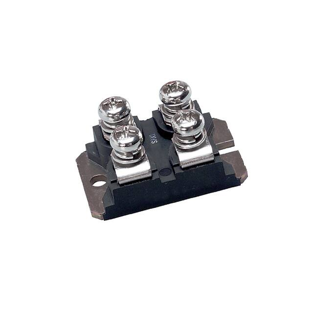
miniBLOC, SOT-227
E153432
S
G
Symbol
Test Conditions
Maximum Ratings
VDSS
TJ = 25C to 150C
75
V
VDGR
TJ = 25C to 150C, RGS = 1M
75
V
VGSS
Continuous
20
V
VGSM
Transient
30
V
ID25
IL(RMS)
IDM
TC = 25C (Chip Capability)
External Lead Current Limit
TC = 25C, pulse width limited by TJM
225
200
720
A
A
A
IA
EAS
TC = 25C
TC = 25C
240
3
A
J
PD
TC = 25C
735
W
TJ
-55...+150
TJM
150
C
-55...+150
C
50/60 Hz, RMS
IISOL 1mA
Md
Mounting Torque
Terminal Connection Torque
G = Gate
S = Source
D = Drain
Either Source Terminal S can be used as
the Source Terminal or the Kelvin Source
(Gate Return) Terminal.
C
Tstg
VISOL
S
D
Features
2500
3000
V~
V~
Designed for Linear Operation
International Standard Package
1.5/13
1.3/11.5
Nm/lb.in
Nm/lb.in
Avalanche Rated
Molding Epoxy Meets UL94 V-0
30
g
t = 1 minute
t = 1 second
Weight
Guaranteed FBSOA at 75°C
Flammability Classification
MiniBLOC with Aluminium Nitride
Isolation
Advantages
Symbol
Test Conditions
(TJ = 25C, unless otherwise specified)
Characteristic Values
Min. Typ. Max.
BVDSS
VGS = 0V, ID = 1mA
75
VGS(th)
VDS = VGS, ID = 3mA
2.0
IGSS
VGS = 20V, VDS = 0V
IDSS
VDS = VDSS, VGS = 0V
RDS(on)
TJ = 125C
VGS = 10V, ID = 120A, Note 1
V
4.5
V
200
nA
Easy to mount
Space savings
High power density
Applications
10 A
50 A
7 m
© 2016 IXYS CORPORATION, All rights reserved
Solid state circuit breakers
Soft start controls
Linear amplifiers
Programmable loads
Current regulators
DS100770(12/16)
�IXTN240N075L2
Symbol
Test Conditions
(TJ = 25C, unless otherwise specified)
Characteristic Values
Min.
Typ.
Max.
gfs
60
VDS = 10V, ID = 60A, Note 1
86
Ciss
Coss
19
VGS = 0V, VDS = 25V, f = 1MHz
Crss
td(on)
tr
td(off)
tf
Resistive Switching Times
VGS = 10V, VDS = 0.5 • VDSS, ID = 120A
RG = 1 (External)
Qg(on)
Qgs
110
VGS = 10V, VDS = 0.5 • VDSS, ID = 120A
Qgd
M4-7 NUT
(4 PLACES)
J
K
S
nF
4420
pF
1470
pF
34
ns
200
ns
136
ns
47
ns
546
nC
86
nC
225
nC
RthJC
TO-227 Outline
B
A
D
T
c
VMWN
S
E
F
G
H
P
NUT MATERIAL:
STANDARD - Low carbon steel with
Ni plating.
OPTIONAL - Brass Nut is available
PART NUMBER-BN
Q
O
R
U
0.17 C/W
RthCS
0.05
C/W
Safe Operating Area Specification
Symbol
Test Conditions
Characteristic Values
Min.
Typ.
Max.
SOA
VDS = 75V, ID = 5.9A, TC = 75C, Tp = 5s
440
W
Source-Drain Diode
Symbol
Test Conditions
(TJ = 25C, unless otherwise specified)
Characteristic Values
Min.
Typ.
Max.
IS
VGS = 0V
240
A
ISM
Repetitive, pulse width limited by TJM
960
A
VSD
IF = 100A, VGS = 0V, Note 1
1.5
V
trr
IRM
QRM
IF = 120A, -di/dt = 100A/s,
VR = 37.5V, VGS = 0V
Note:
206
18.8
1.9
ns
A
μC
1. Pulse test, t 300s; duty cycle, d 2%.
ADVANCE TECHNICAL INFORMATION
The product presented herein is under development. The Technical Specifications offered are
derived from a subjective evaluation of the design, based upon prior knowledge and experience, and constitute a "considered reflection" of the anticipated result. IXYS reserves the right
to change limits, test conditions, and dimensions without notice.
IXYS reserves the right to change limits, test conditions, and dimensions.
IXYS MOSFETs and IGBTs are covered
4,835,592
by one or more of the following U.S. patents: 4,860,072
4,881,106
4,931,844
5,017,508
5,034,796
5,049,961
5,063,307
5,187,117
5,237,481
5,381,025
5,486,715
6,162,665
6,259,123 B1
6,306,728 B1
6,404,065 B1
6,534,343
6,583,505
6,683,344
6,727,585
7,005,734 B2
6,710,405 B2 6,759,692
7,063,975 B2
6,710,463
6,771,478 B2 7,071,537
7,157,338B2
�IXTN240N075L2
Fig. 1. Output Characteristics @ TJ = 25ºC
Fig. 2. Extended Output Characteristics @ TJ = 25ºC
240
VGS = 20V
12V
10V
9V
800
11V
10V
7V
160
I D - Amperes
I D - Amperes
200
VGS = 20V
13V
8V
120
6V
600
9V
8V
400
80
7V
200
40
6V
5V
5V
4V
0
0.0
0.5
1.0
0
1.5
2.0
0
2
4
6
8
VDS - Volts
2.2
240
VGS = 20V
15V
12V
10V
9V
8V
14
16
18
20
VGS = 10V
2.0
7V
R DS(on) - Normalized
I D - Amperes
12
Fig. 4. RDS(on) Normalized to ID = 120A Value vs.
Junction Temperature
Fig. 3. Output Characteristics @ TJ = 125ºC
200
10
VDS - Volts
160
6V
120
80
1.8
1.6
I D = 240A
1.4
I D = 120A
1.2
1.0
5V
40
0.8
4V
0
0.6
0.0
0.5
1.0
1.5
2.0
2.5
-50
3.0
-25
0
Fig. 5. RDS(on) Normalized to ID = 120A Value vs.
Drain Current
75
100
125
150
125
150
220
200
VGS = 10V
20V
External Lead Limit
180
160
2.2
ID - Amperes
RDS(on) - Normalized
50
Fig. 6. Maximum Drain Current vs.
Case Temperature
3.0
2.6
25
TJ - Degrees Centigrade
VDS - Volts
TJ = 125ºC
1.8
140
120
100
80
1.4
60
TJ = 25ºC
40
1.0
20
0.6
0
0
100
200
300
400
500
I D - Amperes
© 2016 IXYS CORPORATION, All rights reserved
600
700
-50
-25
0
25
50
75
TC - Degrees Centigrade
100
�IXTN240N075L2
Fig. 8. Transconductance
Fig. 7. Input Admittance
220
600
TJ = - 40ºC
200
180
TJ = - 40ºC
25ºC
125ºC
400
160
g f s - Siemens
I D - Amperes
500
300
200
25ºC
140
125ºC
120
100
80
60
40
100
20
0
0
3.0
3.5
4.0
4.5
5.0
5.5
6.0
6.5
7.0
7.5
8.0
8.5
0
9.0
100
200
VGS - Volts
Fig. 9. Forward Voltage Drop of Intrinsic Diode
400
500
600
Fig. 10. Gate Charge
10
800
VDS = 37.5V
9
700
I D = 120A
8
I G = 10mA
600
7
TJ = 25ºC
500
VGS - Volts
I S - Amperes
300
I D - Amperes
TJ = 125ºC
400
300
6
5
4
3
200
2
100
1
0
0
0.2
0.4
0.6
0.8
1.0
1.2
1.4
1.6
1.8
2.0
0
2.2
50
100
150
200
250
300
350
400
450
500
550
Fig. 12. Maximum Transient Thermal Impedance
VSD - Volts
QG - NanoCoulombs
1
Fig. 12. Maximum Transient Thermal Impedance
Fig. 11. Capacitance
aaaaa
0.3
100,000
0.1
C iss
Z(th)JC - K / W
Capacitance - PicoFarads
f = 1 MHz
10,000
C oss
0.01
C rss
1,000
0
5
10
15
20
25
30
35
40
VDS - Volts
IXYS reserves the right to change limits, test conditions, and dimensions.
0.001
0.00001
0.0001
0.001
0.01
0.1
Pulse Width - Seconds
1
10
�IXTK240N075L2
Fig. 14. Forward-Bias Safe Operating Area
Fig. 13. Forward-Bias Safe Operating Area
@ TC = 25ºC
@ TC = 75ºC
1,000
1,000
25µs
RDS(on) Limit
RDS(on) Limit
25µs
100µs
100µs
I D - Amperes
1ms
10ms
100ms
10
DC
100
I D - Amperes
100
1ms
10ms
10
100ms
TJ = 150ºC
TJ = 150ºC
TC = 25ºC
Single Pulse
TC = 75ºC
Single Pulse
DC
1
1
1
10
VDS - Volts
© 2016 IXYS CORPORATION, All rights reserved
100
1
10
100
VDS - Volts
IXYS REF: T_240N075L2(9R-T07)12-13-16
�Disclaimer Notice - Information furnished is believed to be accurate and reliable. However, users should independently
evaluate the suitability of and test each product selected for their own applications. Littelfuse products are not designed for,
and may not be used in, all applications. Read complete Disclaimer Notice at www.littelfuse.com/disclaimer-electronics.
�