High Voltage
Power MOSFET
IXTU05N100
IXTY05N100
VDSS
ID25
=
=
RDS(on)
1000V
750mA
17
N-Channel Enhancement Mode
Avalanche Rated
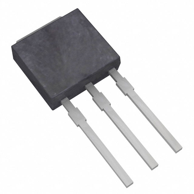
TO-251
(IXTU)
G
D
Symbol
Test Conditions
Maximum Ratings
VDSS
TJ = 25C to 150C
1000
V
VDGR
TJ = 25C to 150C, RGS = 1M
1000
V
VGSS
Continuous
30
V
VGSM
Transient
40
V
ID25
TC = 25C
750
mA
IDM
TC = 25C, Pulse Width Limited by TJM
3
A
IA
TC = 25C
1
A
EAS
TC = 25C
100
mJ
dv/dt
IS IDM, VDD VDSS, TJ 150C
3
V/ns
PD
TC = 25C
40
W
-55 ... +150
150
-55 ... +150
C
C
C
300
260
°C
°C
1.13 / 10
Nm/lb.in.
0.40
0.35
g
g
TJ
TJM
Tstg
TL
TSOLD
Maximum Lead Temperature for Soldering
1.6 mm (0.062in.) from Case for 10s
FC
Mounting force
Weight
TO-251
TO-252
S
D (TAB)
TO-252
(IXTY)
G
S
D (TAB)
G = Gate
S = Source
D
= Drain
TAB = Drain
Features
International Standard Packages
Fast Switching Times
Avalanche Rated
Rds(on) HDMOSTM Process
Rugged Polysilicon Gate Cell structure
Extended FBSOA
Advantages
Symbol
Test Conditions
(TJ = 25C, Unless Otherwise Specified)
Characteristic Values
Min.
Typ.
Max.
BVDSS
VGS = 0V, ID = 250A
1000
VGS(th)
VDS = VGS, ID = 250A
2.5
IGSS
VGS = 30V, VDS = 0V
IDSS
VDS = VDSS, VGS = 0V
RDS(on)
V
4.5
V
100 nA
TJ = 125C
VGS = 10V, ID = 375mA, Note 1
© 2017 IXYS CORPORATION, All Rights Reserved
25 A
500 A
17
High Power Density
Space Savings
Applications
Switch-Mode and Resonant-Mode
Power Supplies
Flyback Inverters
DC Choppers
DS100102B(9/17)
�IXTU05N100
IXTY05N100
Symbol
Test Conditions
(TJ = 25C, Unless Otherwise Specified)
gfs
Characteristic Values
Min.
Typ.
Max.
VDS = 20V, ID = 500mA, Note 1
0.55
Ciss
Coss
VGS = 0V, VDS = 25V, f = 1MHz
Crss
td(on)
tr
td(off)
tf
Resistive Switching Times
VGS = 10V, VDS = 0.5 • VDSS, ID = 1A
RG = 47 (External)
Qg(on)
Qgs
VGS = 10V, VDS = 0.5 • VDSS, ID = 1A
Qgd
TO-251Outline
0.93
S
260
pF
22
pF
8
pF
11
ns
19
ns
40
ns
28
ns
7.8
nC
1.4
nC
4.1
nC
RthJC
1. Gate
3. Source
3.1C/W
Source-Drain Diode
Symbol
Test Conditions
(TJ = 25C, Unless Otherwise Specified)
Characteristic Values
Min.
Typ.
Max.
IS
VGS = 0V
750 mA
ISM
Repetitive, Pulse Width Limited by TJM
VSD
IF = IS, VGS = 0V, Note 1
trr
IF = IS, -di/dt = 100A/s
VR = 100V, VGS = 0V
710
3
A
1.5
V
2.Drain
4. Drain
Dim.
Millimeter
Min.
Max.
Inches
Min. Max.
A
A1
2.19
0.89
2.38
1.14
.086
0.35
.094
.045
b
b1
b2
0.64
0.76
5.21
0.89
1.14
5.46
.025
.030
.205
.035
.045
.215
c
c1
0.46
0.46
0.58
0.58
.018
.018
.023
.023
D
5.97
6.22
.235
.245
E
e
e1
6.35
2.28
4.57
6.73
BSC
BSC
.250
.090
.180
.265
BSC
BSC
H
17.02
17.78
.670
.700
L
L1
L2
8.89
1.91
0.89
9.65
2.28
1.27
.350
.075
.035
.380
.090
.050
TO-252 AA Outline
A
A
E
b3
4
ns
L3
c2
A1
L4
1
2
A2
3
L1
e
e1
e1
b2
L
L2
c
0
5.55MIN
OPTIONAL
H
1 - Gate
2,4 - Drain
3 - Source
6.50MIN
Note 1: Pulse test, t 300s, duty cycle, d 2%.
4
6.40
2.85MIN
BOTTOM
VIEW
2.28
1.25MIN
LAND PATTERN RECOMMENDATION
IXYS Reserves the Right to Change Limits, Test Conditions, and Dimensions.
IXYS MOSFETs and IGBTs are covered
4,835,592
by one or more of the following U.S. patents: 4,860,072
4,881,106
4,931,844
5,017,508
5,034,796
5,049,961
5,063,307
5,187,117
5,237,481
5,381,025
5,486,715
6,162,665
6,259,123 B1
6,306,728 B1
6,404,065 B1
6,534,343
6,583,505
6,683,344
6,727,585
7,005,734 B2
6,710,405 B2 6,759,692
7,063,975 B2
6,710,463
6,771,478 B2 7,071,537
7,157,338B2
�IXTU05N100
IXTY05N100
o
o
Fig. 2. Output Characteristics @ TJ = 125 C
Fig. 1. Output Characteristics @ TJ = 25 C
0.9
1.4
VGS = 10V
8V
1.2
0.7
7V
I D - Amperes
I D - Amperes
1.0
6.5V
0.8
VGS = 10V
7V
6V
0.8
0.6
0.6
5.5V
0.5
0.4
0.3
5V
0.4
0.2
6V
0.2
0.1
5V
0.0
0
2.8
2.6
4
8
12
16
20
4.5V
0.0
24
28
0
32
4
8
12
16
20
28
VDS - Volts
Fig. 3. RDS(on) Normalized to ID = 0.35A Value
vs. Junction Temperature
Fig. 4. RDS(on) Normalized to ID = 0.35A Value
vs. Drain Current
2.6
VGS = 10V
VGS = 10V
2.4
32
o
TJ = 125 C
2.4
2.2
2.0
RDS(on) - Normalized
2.2
RDS(on) - Normalized
24
VDS - Volts
I D = 0.75A
1.8
1.6
I D = 0.35A
1.4
1.2
1.0
2.0
1.8
1.6
o
TJ = 25 C
1.4
1.2
0.8
1.0
0.6
0.8
0.4
-50
-25
0
25
50
75
100
125
0
150
0.2
0.4
0.6
0.8
1
1.2
1.4
I D - Amperes
TJ - Degrees Centigrade
Fig. 5. Maximum Drain Current vs. Case Temperature
Fig. 6. Input Admittance
0.8
1.1
1.0
0.7
0.9
0.8
0.5
I D - Amperes
I D - Amperes
0.6
0.4
0.3
0.7
0.6
o
TJ = 125 C
0.5
o
25 C
o
- 40 C
0.4
0.3
0.2
0.2
0.1
0.1
0
0.0
-50
-25
0
25
50
75
TC - Degrees Centigrade
© 2017 IXYS CORPORATION, All Rights Reserved
100
125
150
3.0
3.5
4.0
4.5
5.0
VGS - Volts
5.5
6.0
6.5
�IXTU05N100
IXTY05N100
Fig. 7. Transconductance
Fig. 8. Forward Voltage Drop of Intrinsic Diode
1.6
2.5
o
TJ = - 40 C
1.4
2.0
1.2
o
25 C
I S - Amperes
g f s - Siemens
1.0
o
125 C
0.8
0.6
1.5
1.0
o
TJ = 125 C
0.4
o
TJ = 25 C
0.5
0.2
0.0
0.0
0
0.2
0.4
0.6
0.8
1
1.2
0.3
0.4
0.5
I D - Amperes
Fig. 9. Gate Charge
0.7
0.8
0.9
Fig. 10. Capacitance
10
1,000
f = 1 MHz
VDS = 500V
9
I D = 1A
8
Capacitance - PicoFarads
I G = 1mA
7
VGS - Volts
0.6
VSD - Volts
6
5
4
3
Ciss
100
Coss
10
Crss
2
1
1
0
10
1
2
3
4
5
6
7
5
10
15
20
25
30
35
QG - NanoCoulombs
VDS - Volts
Fig. 11. Forward-Bias Safe Operating Area
o
@ TC = 25 C
Fig. 12. Forward-Bias Safe Operating Area
o
@ TC = 75 C
10
RDS(on) Limit
- Amperes
D
1ms
0.1
10ms
o
TJ = 150 C
DC
o
TC = 25 C
Single Pulse
25μs
1
100μs
1ms
0.1
100ms
0.01
40
RDS(on) Limit
100μs
1
I
0
8
I D - Amperes
0
10ms
o
TJ = 150 C
100ms
o
TC = 75 C
Single Pulse
DC
0.01
10
100
1,000
VDS - Volts
IXYS Reserves the Right to Change Limits, Test Conditions, and Dimensions.
10
100
VDS - Volts
1,000
�IXTU05N100
IXTY05N100
Fig. 13. Maximum Transient Thermal Impedance
Z (th)JC - K / W
10
1
0.1
0.0001
0.001
0.01
0.1
1
Pulse Width - Second
© 2017 IXYS CORPORATION, All Rights Reserved
IXYS REF: T_05N100(1T) 5-13-14-A
�Disclaimer Notice - Information furnished is believed to be accurate and reliable. However, users should independently
evaluate the suitability of and test each product selected for their own applications. Littelfuse products are not designed for,
and may not be used in, all applications. Read complete Disclaimer Notice at www.littelfuse.com/disclaimer-electronics.
�