High Voltage
Power MOSFET
IXTU01N100
IXTY01N100
VDSS
ID25
=
=
RDS(on)
1000V
100mA
80
N-Channel Enhancement Mode
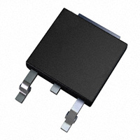
TO-251
(IXTU)
G
D
Symbol
Test Conditions
VDSS
TJ = 25C to 150C
1000
V
VDGR
TJ = 25C to 150C, RGS = 1M
1000
V
VGSS
Continuous
20
V
VGSM
Transient
30
V
ID25
TC = 25C
100
mA
IDM
TC = 25C, Pulse Width Limited by TJM
400
mA
PD
TC = 25C
25
W
-55 ... +150
150
-55 ... +150
C
C
C
300
260
°C
°C
1.13 / 10
Nm/lb.in.
0.40
0.35
g
g
TJ
TJM
Tstg
TL
TSOLD
Maximum Lead Temperature for Soldering
1.6 mm (0.062in.) from Case for 10s
FC
Mounting force
Weight
TO-251
TO-252
Maximum Ratings
S
D (Tab)
TO-252
(IXTY)
G
S
D (Tab)
G = Gate
S = Source
D
= Drain
Tab = Drain
Features
International Standard Packages
Fast Switching Times
Avalanche Rated
Rds(on) HDMOSTM Process
Rugged Polysilicon Gate Cell structure
Advantages
Symbol
Test Conditions
(TJ = 25C, Unless Otherwise Specified)
Characteristic Values
Min.
Typ.
Max.
BVDSS
VGS = 0V, ID = 25A
1000
VGS(th)
VDS = VGS, ID = 25A
2.0
IGSS
VGS = 20V, VDS = 0V
IDSS
VDS = 0.8 • VDSS, VGS = 0V
TJ = 125C
RDS(on)
VGS = 10V, ID = 50mA, Note 1
© 2017 IXYS CORPORATION, All Rights Reserved
V
4.5
10 A
200 A
80
Applications
V
50 nA
60
High Power Density
Space Savings
Level Shifting
Triggers
Solid State Relays
Current Regulators
DS98812E(9/17)
�IXTU01N100
IXTY01N100
Symbol
Test Conditions
(TJ = 25C, Unless Otherwise Specified)
gfs
Characteristic Values
Min.
Typ.
Max.
VDS = 10V, ID = 50mA, Note 1
Ciss
Coss
VGS = 0V, VDS = 25V, f = 1MHz
Crss
td(on)
tr
td(off)
tf
Resistive Switching Times
VGS = 10V, VDS = 0.5 • VDSS, ID = 50mA
RG = 50 (External)
Qg(on)
Qgs
VGS = 10V, VDS = 0.5 • VDSS, ID = 50mA
Qgd
TO-251 Outline
0.16
S
54.0
pF
6.9
pF
2.0
pF
12
ns
12
ns
40
28
ns
ns
6.9
nC
1.8
nC
3.0
nC
RthJC
1. Gate
3. Source
5C/W
Source-Drain Diode
Symbol
Test Conditions
(TJ = 25C, Unless Otherwise Specified)
Characteristic Values
Min.
Typ.
Max.
IS
VGS = 0V
100 mA
ISM
Repetitive, Pulse Width Limited by TJM
300 mA
VSD
IF = IS, VGS = 0V, Note 1
1.8
V
trr
IF = 0.75A, -di/dt = 100A/μs,
VR = 25V
1.5
μs
2.Drain
4. Drain
Dim.
Millimeter
Min.
Max.
Inches
Min. Max.
A
A1
2.19
0.89
2.38
1.14
.086
0.35
.094
.045
b
b1
b2
0.64
0.76
5.21
0.89
1.14
5.46
.025
.030
.205
.035
.045
.215
c
c1
0.46
0.46
0.58
0.58
.018
.018
.023
.023
D
5.97
6.22
.235
.245
E
e
e1
6.35
2.28
4.57
6.73
BSC
BSC
.250
.090
.180
.265
BSC
BSC
H
17.02
17.78
.670
.700
L
L1
L2
8.89
1.91
0.89
9.65
2.28
1.27
.350
.075
.035
.380
.090
.050
TO-252 AA Outline
A
A
E
b3
4
L3
c2
A1
L4
1
2
A2
3
L1
e
e1
e1
b2
L
L2
c
0
5.55MIN
OPTIONAL
H
1 - Gate
2,4 - Drain
3 - Source
6.50MIN
Note 1: Pulse test, t 300s, duty cycle, d 2%.
4
6.40
2.85MIN
BOTTOM
VIEW
2.28
1.25MIN
LAND PATTERN RECOMMENDATION
IXYS Reserves the Right to Change Limits, Test Conditions, and Dimensions.
IXYS MOSFETs and IGBTs are covered
4,835,592
by one or more of the following U.S. patents: 4,860,072
4,881,106
4,931,844
5,017,508
5,034,796
5,049,961
5,063,307
5,187,117
5,237,481
5,381,025
5,486,715
6,162,665
6,259,123 B1
6,306,728 B1
6,404,065 B1
6,534,343
6,583,505
6,683,344
6,727,585
7,005,734 B2
6,710,405 B2 6,759,692
7,063,975 B2
6,710,463
6,771,478 B2 7,071,537
7,157,338B2
�IXTU01N100
IXTY01N100
o
o
Fig. 2. ExtendedOutput Characteristics @ TJ = 25 C
Fig. 1. Output Characteristics @ TJ = 25 C
500
200
VGS = 10V
180
6V
400
140
I D - MilliAmperes
I D - MilliAmperes
160
120
100
80
60
VGS = 10V
450
6V
350
300
250
200
150
5V
40
100
20
50
5V
0
0
0
2
4
6
8
10
12
0
14
5
10
15
20
3.0
200
VGS = 10V
35
40
45
50
VGS = 10V
2.6
6V
160
140
RDS(on) - Normalized
I D - MilliAmperes
30
Fig. 3. RDS(on) Normalized to ID = 50mA Value
vs. Junction Temperature
o
Fig. 2. Output Characteristics @ TJ = 125 C
180
25
VDS - Volts
VDS - Volts
120
5V
100
80
60
2.2
I D = 200mA
1.8
I D = 100mA
1.4
1.0
40
0.6
20
0.2
0
0
5
10
15
20
25
-50
30
-25
0
Fig. 4. RDS(on) Normalized to ID = 50mA Value
vs. Drain Current
3.0
VGS = 10V
75
100
125
150
Fig. 5. Maximum Drain Current vs. Case Temperature
o
100
I D - MilliAmperes
RDS(on) - Normalized
50
120
TJ = 125 C
2.6
25
TJ - Degrees Centigrade
VDS - Volts
2.2
o
TJ = 25 C
1.8
1.4
80
60
40
20
1.0
0
0.6
0
50
100
150
200
250
300
350
I D - MilliAmperes
© 2017 IXYS CORPORATION, All Rights Reserved
400
450
500
-50
-25
0
25
50
75
TC - Degrees Centigrade
100
125
150
�IXTU01N100
IXTY01N100
Fig. 7. Input Admittance
Fig. 8. Transconductance
160
o
350
140
TJ = - 40 C
VDS = 10V
VDS = 10V
300
o
25 C
250
100
g f s - Siemens
I D - MilliAmperes
120
80
60
o
TJ = 125 C
o
TJ = 25 C
40
200
o
125 C
150
100
50
20
0
0
3.2
3.6
4.0
4.4
4.8
5.2
5.6
0
20
40
60
VGS - Volts
120
140
160
6
7
8
10
VDS = 500V
9
350
I D = 50mA
8
300
I G = 1mA
7
250
V GS - Volts
I S - MilliAmperes
100
Fig. 10. Gate Charge
Fig. 9. Forward Voltage Drop of Intrinsic Diode
400
200
150
o
TJ = 125 C
6
5
4
3
o
TJ = 25 C
100
2
50
1
0
0
0.3
0.4
0.5
0.6
0.7
0.8
0
0.9
1
2
3
4
5
QG - NanoCoulombs
VSD - Volts
Fig. 12. Maximum Transient Thermal Impedance
Fig. 11. Capacitance
100
10
Ciss
10
Z (th)JC - K / W
Capacitance - PicoFarads
80
I D - MilliAmperes
Coss
1
Crss
f = 1 MHz
1
0
5
10
15
20
25
30
35
40
VDS - Volts
0.1
0.00001
0.0001
0.001
0.01
0.1
1
Pulse Width - Second
IXYS Reserves the Right to Change Limits, Test Conditions, and Dimensions.
IXYS REF: T_01N100(1N) 8-18-05-A
�