IXYH55N120A4
1200V XPTTM
GenX4TM IGBT
VCES =
IC110 =
VCE(sat)
tfi(typ) =
Ultra Low-Vsat PT IGBT for
up to 5kHz Switching
1200V
55A
1.8V
270ns
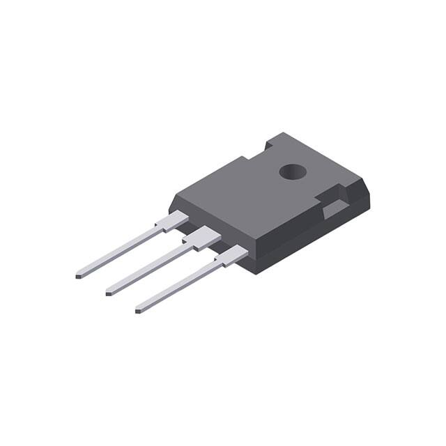
TO-247
(IXYH)
Symbol
Test Conditions
VCES
VCGR
TJ = 25°C to 175°C
TJ = 25°C to 175°C, RGE = 1M
VGES
VGEM
G
Maximum Ratings
1200
1200
V
V
Continuous
Transient
±20
±30
V
V
IC25
IC110
ICM
TC = 25°C
TC = 110°C
TC = 25°C, 1ms
175
55
350
A
A
A
SSOA
(RBSOA)
VGE = 15V, TVJ = 125°C, RG = 5
Clamped Inductive Load
ICM = 110
0.8 • VCES
A
PC
TC = 25°C
650
W
-55 ... +175
175
-55 ... +175
°C
°C
°C
300
°C
VCE
TJ
TJM
Tstg
TL
Md
Maximum Lead Temperature for Soldering
1.6 mm (0.062 in.) from Case for 10s
Nm/lb.in
6
g
Weight
BVCES
IC
= 250A, VGE = 0V
1200
VGE(th)
IC
= 250A, VCE = VGE
4.0
ICES
VCE = VCES, VGE = 0V
6.5
VCE = 0V, VGE = 20V
VCE(sat)
IC
= 55A, VGE = 15V, Note 1
TJ = 150C
©2020 Littelfuse, Inc.
V
5 A
2.5 mA
TJ = 150C
IGES
V
100
1.5
1.8
1.8
Optimized for Low Conduction Losses
Positive Thermal Coefficient of
Vce(sat)
International Standard Package
High Power Density
Low Gate Drive Requirement
Applications
Characteristic Values
Min.
Typ.
Max.
C
= Collector
Tab = Collector
Advantages
Symbol
Test Conditions
(TJ = 25C, Unless Otherwise Specified)
C (Tab)
Features
1.13 / 10
E
G = Gate
E = Emitter
Mounting Torque
C
Power Inverters
UPS
Motor Drives
SMPS
PFC Circuits
Battery Chargers
Welding Machines
Lamp Ballasts
Inrush Current Protector Circuits
nA
V
V
DS100983C(4/20)
�IXYH55N120A4
Symbol Test Conditions
(TJ = 25°C Unless Otherwise Specified)
Characteristic Values
Min.
Typ.
Max.
gfs
22
IC = 55A, VCE = 10V, Note 1
Cies
Coes
Cres
VCE = 25V, VGE = 0V, f = 1MHz
Qg(on)
Qge
Qgc
IC = 55A, VGE = 15V, VCE = 0.5 • VCES
td(on)
tri
Eon
td(off)
tfi
Eoff
td(on)
tri
Eon
td(off)
tfi
Eoff
Inductive load, TJ = 25°C
IC = 40A, VGE = 15V
VCE = 0.5 • VCES, RG = 5
Note 2
Inductive load, TJ = 150°C
IC = 40A, VGE = 15V
VCE = 0.5 • VCES, RG = 5
Note 2
36
S
2150
125
80
pF
pF
pF
110
17
56
nC
nC
nC
23
35
2.3
300
270
5.3
ns
ns
mJ
ns
ns
mJ
21
33
3.8
380
530
8.8
ns
ns
mJ
ns
ns
mJ
0.21
0.23 °C/W
C/W
RthJC
RthCS
Notes:
1. Pulse test, t 300µs, duty cycle, d 2%.
2. Switching times & energy losses may increase for higher VCE(clamp), TJ or RG.
Littelfuse Reserves the Right to Change Limits, Test Conditions, and Dimensions.
IXYS MOSFETs and IGBTs are covered
4,835,592
by one or more of the following U.S. patents: 4,860,072
4,881,106
4,931,844
5,017,508
5,034,796
5,049,961
5,063,307
5,187,117
5,237,481
5,381,025
5,486,715
6,162,665
6,259,123 B1
6,306,728 B1
6,404,065 B1
6,534,343
6,583,505
6,683,344
6,727,585
7,005,734 B2
6,710,405 B2 6,759,692
7,063,975 B2
6,710,463
6,771,478 B2 7,071,537
7,157,338B2
�IXYH55N120A4
Fig. 1. Output Characteristics @ TJ = 25oC
Fig. 2. Extended Output Characteristics @ TJ = 25oC
VGE = 15V
13V
12V
11V
100
300
10V
V GE = 15V
250
14V
I C - Amperes
I C - Amperes
80
9V
60
8V
40
200
13V
12V
150
11V
10V
100
9V
20
0
0
0.5
1
1.5
2
7V
50
8V
6V
0
7V
6V
2.5
3
0
5
15
20
Fig. 3. Output Characteristics @ TJ = 150oC
Fig. 4. Dependence of VCE(sat) on
Junction Temperature
2.0
VGE = 15V
13V
12V
11V
10V
60
9V
8V
40
V GE = 15V
1.8
VCE(sat) - Normalized
80
I C = 110A
1.6
1.4
I C = 55A
1.2
1.0
7V
20
0.8
I C = 27.5A
6V
0
0.6
0
0.5
4.5
1
1.5
2
2.5
3
3.5
-50
-25
0
25
50
75
100
VCE - Volts
TJ - Degrees Centigrade
Fig. 5. Collector-to-Emitter Voltage vs.
Gate-to-Emitter Voltage
Fig. 6. Input Admittance
125
150
175
100
o
TJ = 25 C
4.0
80
I C - Amperes
3.5
VCE - Volts
25
VCE - Volts
100
I C - Amperes
10
VCE - Volts
3.0
I C = 110A
2.5
60
40
o
2.0
TJ = 150 C
55A
o
25 C
20
1.5
o
- 40 C
27.5A
1.0
0
7
8
9
10
11
VGE - Volts
©2020 Littelfuse, Inc.
12
13
14
15
4
5
6
7
VGE - Volts
8
9
10
�IXYH55N120A4
Fig. 7. Transconductance
50
Fig. 8. Gate Charge
16
o
TJ = - 40 C
45
VCE = 600V
14
I C = 55A
40
I G = 10mA
12
o
25 C
30
VGE - Volts
g f s - Siemens
35
o
150 C
25
20
10
8
6
15
4
10
2
5
0
0
0
20
40
60
80
100
120
0
20
40
I C - Amperes
80
100
120
Fig. 10. Reverse-Bias Safe Operating Area
Fig. 9. Capacitance
10,000
120
Cies
100
1,000
80
Coes
I C - Amperes
Capacitance - PicoFarads
60
QG - NanoCoulombs
100
60
40
o
TJ = 125 C
Cres
20
f = 1 MHz
10
RG = 5Ω
dv / dt < 10V / ns
0
0
5
10
15
20
25
35
40
200
300
400
500
Fig.3011. Maximum
Transient Thermal
Impedance
VCE - Volts
1
600
700
800
900
1000
1100
1200
VCE - Volts
Fig. 11. Maximum Transient Thermal Impedance
aaa
0.4
Z(th)JC - K / W
0.1
0.01
0.001
0.00001
0.0001
0.001
0.01
Pulse Width - Seconds
Littelfuse Reserves the Right to Change Limits, Test Conditions, and Dimensions.
0.1
1
10
�IXYH55N120A4
Fig. 12. Inductive Switching Energy Loss vs.
Collector Current
20
Eoff
18
16
Eon
9
VCE = 600V
5
8
4
6
3
o
TJ = 25 C
Eoff - MilliJoules
10
2
2
1
0
18
40
50
6
o
TJ = 150 C
10
5
8
4
3
TJ = 25 C
4
60
70
2
2
400
80
500
600
700
800
900
I C - Amperes
VCE - Volts
Fig. 14. Inductive Switching Energy Loss vs.
Gate Resistance
Fig. 15. Inductive Switching Energy Loss vs.
Junction Temperature
Eoff
16
14
Eon
o
TJ = 150 C , VGE = 15V
16
I C = 40A
6
0
30
7
o
4
20
Eon
Eoff
14
12
1
1000
14
Eon
12
RG = 5Ω,VGE = 15V
I C = 80A
VCE = 600V
VCE = 600V
8
10
6
Eoff - MilliJoules
12
10
10
8
6
6
8
4
2
10
12
14
16
18
2
20
25
50
75
100
125
TJ - Degrees Centigrade
Fig. 16. Inductive Turn-off Switching Times vs.
Gate Resistance
Fig. 17. Inductive Turn-off Switching Times vs.
Collector Current
600
td(off)
1000
tfi
550
o
TJ = 150 C, VGE = 15V
560
400
540
350
I C = 40A
520
300
500
500
600
400
o
TJ = 150 C
400
300
o
TJ = 25 C
200
200
250
480
200
4
6
8
10
12
RG - Ohms
©2020 Littelfuse, Inc.
14
16
18
20
0
100
20
30
40
50
I C - Amperes
60
70
80
t d(off) - Nanoseconds
I C = 80A
t d(off) - Nanoseconds
450
600
td(off)
VCE = 600V
500
580
0
150
RG = 5Ω,VGE = 15V
800
I C = 40A
VCE = 600V
600
2
RG - Ohms
tfi
620
t f i - Nanoseconds
8
t f i - Nanoseconds
640
6
4
I C = 40A
4
I C = 40A
6
8
I C = 80A
Eon - MilliJoules
10
Eon - MilliJoules
Eoff - MilliJoules
12
14
4
Eon - MilliJoules
6
Eon - MilliJoules
o
TJ = 150 C
8
RG = 5Ω,VGE = 15V
12
7
12
Eoff
14
8
14
E off - MilliJoules
16
10
RG = 5Ω,VGE = 15V
Fig. 13. Inductive Switching Energy Loss vs.
Collector-Emitter Voltage
�IXYH55N120A4
Fig. 18. Inductive Turn-off Switching Times vs.
Junction Temperature
700
tfi
600
450
Fig. 19. Inductive Turn-on Switching Times vs.
Gate Resistance
200
td(off)
tri
400
RG = 5Ω, VGE = 15V
160
200
100
50
75
100
125
t r i - Nanoseconds
150
150
0
10
4
6
8
10
12
14
16
18
Fig. 21. Inductive Turn-on Switching Times vs.
Junction Temperature
130
36
tri
td(on)
110
24
20
20
o
TJ = 150 C
0
16
30
40
50
60
70
40
90
35
I C = 80A
70
30
50
25
30
20
I C = 40A
10
80
I C - Amperes
25
50
t d(on) - Nanoseconds
o
TJ = 25 C
45
VCE = 600V
t d(on) - Nanoseconds
28
20
td(on)
RG = 5Ω, VGE = 15V
32
60
20
20
Fig. 20. Inductive Turn-on Switching Times vs.
Collector Current
VCE = 600V
30
I C = 40A
RG - Ohms
RG = 5Ω, VGE = 15V
40
80
TJ - Degrees Centigrade
tri
80
40
40
200
100
t r i - Nanoseconds
120
t r i - Nanoseconds
t f i - Nanoseconds
250
I C = 80A
t d(on) - Nanoseconds
I C = 80A
300
t d(off) - Nanoseconds
300
I C = 40A
25
50
VCE = 600V
350
400
td(on)
o
TJ = 150 C, VGE = 15V
VCE = 600V
500
60
75
100
125
15
150
TJ - Degrees Centigrade
Littelfuse Reserves the Right to Change Limits, Test Conditions, and Dimensions.
IXYS REF: IXY_55N120A4 (Y17-RY90) 8-01-19
�IXYH55N120A4
TO-247 Outline
1 - Gate
2,4 - Collector
3 - Emitter
©2020 Littelfuse, Inc.
�IXYH55N120A4
Disclaimer Notice - Information furnished is believed to be accurate and reliable. However, users should independently
evaluate the suitability of and test each product selected for their own applications. Littelfuse products are not designed for,
and may not be used in, all applications. Read complete Disclaimer Notice at www.littelfuse.com/disclaimer-electronics.
Littelfuse Reserves the Right to Change Limits, Test Conditions, and Dimensions.
�


 工商网监
湘ICP备2023018690号
工商网监
湘ICP备2023018690号
