Preliminary Technical Information
IXYP15N65C3
XPTTM 650V IGBT
GenX3TM
VCES =
IC110 =
VCE(sat)
tfi(typ) =
Extreme Light Punch Through
IGBT for 20-60kHz Switching
650V
15A
2.5V
28ns
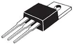
TO-220
Symbol
Test Conditions
Maximum Ratings
VCES
VCGR
TJ = 25°C to 175°C
TJ = 25°C to 175°C, RGE = 1M
650
650
V
V
VGES
VGEM
Continuous
Transient
±20
±30
V
V
IC25
IC110
ICM
TC = 25°C
TC = 110°C
TC = 25°C, 1ms
38
15
80
A
A
A
IA
EAS
TC = 25°C
TC = 25°C
5
100
A
mJ
SSOA
(RBSOA)
VGE = 15V, TVJ = 150°C, RG = 20
Clamped Inductive Load
ICM = 30
@VCE VCES
A
tsc
(SCSOA)
VGE = 15V, VCE = 360V, TJ = 150°C
RG = 82, Non Repetitive
8
μs
PC
TC = 25°C
Maximum Lead Temperature for Soldering
1.6 mm (0.062in.) from Case for 10s
Md
Mounting Torque
W
-55 ... +175
175
-55 ... +175
°C
°C
°C
300
260
°C
°C
1.13/10
Nm/lb.in.
3
g
Weight
BVCES
IC
= 250A, VGE = 0V
650
VGE(th)
IC
= 250A, VCE = VGE
3.5
ICES
VCE = VCES, VGE = 0V
VCE = 0V, VGE = 20V
VCE(sat)
IC
= 15A, VGE = 15V, Note 1
TJ = 150C
© 2014 IXYS CORPORATION, All Rights Reserved
6.0
V
10
150
A
A
100
nA
TJ = 150C
IGES
V
1.96
2.45
2.50
Optimized for 20-60kHz Switching
Square RBSOA
Avalanche Rated
Short Circuit Capability
International Standard Package
High Power Density
Extremely Rugged
Low Gate Drive Requirement
Applications
Characteristic Values
Min.
Typ.
Max.
C = Collector
Tab = Collector
Advantages
Symbol
Test Conditions
(TJ = 25C, Unless Otherwise Specified)
Tab
Features
200
CE
G = Gate
E = Emitter
TJ
TJM
Tstg
TL
TSOLD
G
Power Inverters
UPS
Motor Drives
SMPS
PFC Circuits
Battery Chargers
Welding Machines
Lamp Ballasts
High Frequency Power Inverters
V
V
DS100542A(7/14)
�IXYP15N65C3
Symbol Test Conditions
(TJ = 25°C Unless Otherwise Specified)
Characteristic Values
Min.
Typ.
Max.
gfs
5.0
IC = 15A, VCE = 10V, Note 1
Cies
Coes
Cres
VCE = 25V, VGE = 0V, f = 1MHz
Qg(on)
Qge
Qgc
IC = 15A, VGE = 15V, VCE = 0.5 • VCES
td(on)
tri
Eon
td(off)
tfi
Eoff
td(on)
tri
Eon
td(off)
tfi
Eoff
Inductive load, TJ = 25°C
IC = 15A, VGE = 15V
VCE = 400V, RG = 20
Note 2
Inductive load, TJ = 150°C
IC = 15A, VGE = 15V
VCE = 400V, RG = 20
Note 2
RthJC
RthCS
Notes:
TO-220 (IXYP) Outline
8.5
S
583
37
13
pF
pF
pF
19
4
10
nC
nC
nC
15
20
0.27
68
28
0.23
ns
ns
mJ
ns
ns
mJ
0.40
15
21
0.53
80
42
0.24
ns
ns
mJ
ns
ns
mJ
0.50
0.75 °C/W
°C/W
Pins:
1 - Gate
2 - Collector
3 - Emitter
1. Pulse test, t 300μs, duty cycle, d 2%.
2. Switching times & energy losses may increase for higher VCE(clamp), TJ or RG.
PRELIMANARY TECHNICAL INFORMATION
The product presented herein is under development. The Technical Specifications offered are
derived from a subjective evaluation of the design, based upon prior knowledge and experience, and constitute a "considered reflection" of the anticipated result. IXYS reserves the right
to change limits, test conditions, and dimensions without notice.
IXYS Reserves the Right to Change Limits, Test Conditions, and Dimensions.
IXYS MOSFETs and IGBTs are covered
4,835,592
by one or more of the following U.S. patents: 4,860,072
4,881,106
4,931,844
5,017,508
5,034,796
5,049,961
5,063,307
5,187,117
5,237,481
5,381,025
5,486,715
6,162,665
6,259,123 B1
6,306,728 B1
6,404,065 B1
6,534,343
6,583,505
6,683,344
6,727,585
7,005,734 B2
6,710,405 B2 6,759,692
7,063,975 B2
6,710,463
6,771,478 B2 7,071,537
7,157,338B2
�IXYP15N65C3
Fig. 1. Output Characteristics @ T J = 25ºC
Fig. 2. Extended Output Characteristics @ T J = 25ºC
30
VGE = 15V
14V
13V
12V
25
VGE = 15V
60
15
10V
10
14V
50
11V
20
IC - Amperes
IC - Amperes
70
13V
40
12V
30
11V
9V
20
8V
10
7V
0
10V
5
0
0
0.5
1
1.5
2
2.5
3
3.5
9V
8V
0
5
10
15
25
30
Fig. 4. Dependence of VCE(sat) on
Junction Temperature
Fig. 3. Output Characteristics @ T J = 150ºC
30
2.0
VGE = 15V
14V
13V
12V
25
VGE = 15V
1.8
VCE(sat) - Normalized
11V
20
IC - Amperes
20
VCE - Volts
VCE - Volts
10V
15
9V
10
1.6
I
1.4
I
1.2
C
= 15A
1.0
I
8V
5
= 30A
C
C
= 7.5A
0.8
7V
0.6
0
0
0.5
1
1.5
2
2.5
3
3.5
4
-50
4.5
-25
0
25
VCE - Volts
Fig. 5. Collector-to-Emitter Voltage vs.
Gate-to-Emitter Voltage
75
100
125
150
175
12
13
Fig. 6. Input Admittance
40
8
TJ = 25ºC
7
35
30
IC - Amperes
6
VCE - Volts
50
TJ - Degrees Centigrade
5
I
C
= 7.5A
15A
30A
4
3
25
20
TJ = 150ºC
25ºC
- 40ºC
15
10
2
5
1
0
8
9
10
11
12
VGE - Volts
© 2014 IXYS CORPORATION, All Rights Reserved
13
14
15
5
6
7
8
9
VGE - Volts
10
11
�IXYP15N65C3
Fig. 8. Gate Charge
Fig. 7. Transconductance
16
11
TJ = - 40ºC
10
9
25ºC
150ºC
VGE - Volts
7
I C = 15A
I G = 10mA
12
8
g f s - Siemens
VCE = 325V
14
6
5
10
8
4
6
3
4
2
2
1
0
0
0
5
10
15
20
25
30
0
35
2
4
6
8
10
12
14
16
18
20
QG - NanoCoulombs
IC - Amperes
Fig. 9. Capacitance
Fig. 10. Reverse-Bias Safe Operating Area
35
1,000
30
Capacitance - PicoFarads
Cies
IC - Amperes
25
100
Coes
20
15
10
TJ = 150ºC
5
Cres
f = 1 MHz
10
0
5
10
15
20
25
30
35
40
RG = 20Ω
dv / dt < 10V / ns
0
100
200
300
VCE - Volts
400
500
600
700
VCE - Volts
Fig. 11. Maximum Transient Thermal Impedance
Z(th)JC - ºC / W
1
0.1
0.01
0.00001
0.0001
0.001
Pulse Width - Second
IXYS Reserves the Right to Change Limits, Test Conditions, and Dimensions.
0.01
0.1
1
�IXYP15N65C3
Fig. 13. Inductive Switching Energy Loss vs.
Collector Current
Fig. 12. Inductive Switching Energy Loss vs.
Gate Resistance
1.0
Eon -
---
0.8
1.8
Eoff
0.8
TJ = 150ºC , VGE = 15V
4
VCE = 400V
0.4
2
I
0.2
C
= 15A
----
1.6
1.4
VCE = 400V
0.6
1.2
0.5
1.0
TJ = 150ºC
0.4
0.8
0.3
0.6
0.2
1
0.4
TJ = 25ºC
0.1
0.0
20
30
40
50
60
70
80
90
0.2
0.0
0
100
0.0
8
10
12
14
16
Fig. 14. Inductive Switching Energy Loss vs.
Junction Temperature
1.0
2.0
1.5
I C = 30A
0.4
1.0
0.2
0.5
I C = 15A
0.0
75
100
160
40
140
35
I
25
80
20
60
50
110
45
30
40
50
80
90
40
100
tfi
15
IC - Amperes
© 2014 IXYS CORPORATION, All Rights Reserved
28
30
VCE = 400V
t f i - Nanoseconds
80
35
75
I C = 15A
30
70
25
65
I
C
= 30A
50
15
55
40
10
20
26
85
60
60
24
td(off) - - - -
20
25
22
70
25
50
75
100
TJ - Degrees Centigrade
125
50
150
t d(off) - Nanoseconds
70
20
60
90
40
100
80
18
120
RG = 20Ω , VGE = 15V
TJ = 25ºC
16
= 30A
100
20
t d(off) - Nanoseconds
t f i - Nanoseconds
td(off) - - - -
35
14
C
30
120
90
12
= 15A
45
RG = 20Ω , VGE = 15V
40
10
C
Fig. 17. Inductive Turn-off Switching Times vs.
Junction Temperature
VCE = 400V
8
220
RG - Ohms
tfi
30
30
180
I
15
0.0
150
125
55
45
28
200
VCE = 400V
Fig. 16. Inductive Turn-off Switching Times vs.
Collector Current
TJ = 150ºC
26
td(off) - - - -
TJ - Degrees Centigrade
50
24
t d(off) - Nanoseconds
0.6
50
22
TJ = 150ºC, VGE = 15V
50
t f i - Nanoseconds
VCE = 400V
25
tfi
55
E on - MilliJoules
E off - MilliJoules
----
RG = 20Ω , VGE = 15V
0.8
20
Fig. 15. Inductive Turn-off Switching Times vs.
Gate Resistance
60
2.5
Eon
18
IC - Amperes
RG - Ohms
Eoff
Eon - MilliJoules
3
0.7
Eon - MilliJoules
I C = 30A
0.6
Eon
RG = 20Ω , VGE = 15V
Eoff - MilliJoules
Eoff
Eoff - MilliJoules
0.9
5
�IXYP15N65C3
Fig. 19. Inductive Turn-on Switching Times vs.
Collector Current
Fig. 18. Inductive Turn-on Switching Times vs.
Gate Resistance
160
60
80
tri
140
td(on) - - - -
70
C
= 30A
40
60
30
40
20
I
20
C
= 15A
10
0
30
40
50
60
70
t r i - Nanoseconds
t r i - Nanoseconds
I
80
80
90
40
18
TJ = 125ºC, 25ºC
30
16
20
14
10
12
0
0
100
t d(on) - Nanoseconds
50
20
VCE = 400V
t d(on) - Nanoseconds
100
td(on) - - - -
RG = 20Ω , VGE = 15V
60
VCE = 400V
20
tri
50
TJ = 150ºC, VGE = 15V
120
22
10
8
10
12
14
16
18
20
22
24
26
28
30
IC - Amperes
RG - Ohms
Fig. 20. Inductive Turn-on Switching Times vs.
Junction Temperature
70
19
tri
60
td(on) - - - 18
RG = 20Ω , VGE = 15V
I
C
= 30A
50
17
40
16
30
15
I C = 15A
20
14
10
25
50
75
100
t d(on) - Nanoseconds
t r i - Nanoseconds
VCE = 400V
125
13
150
TJ - Degrees Centigrade
IXYS Reserves the Right to Change Limits, Test Conditions, and Dimensions.
IXYS REF: IXY_15N65C3(31)5-21-13
�Disclaimer Notice - Information furnished is believed to be accurate and reliable. However, users should independently
evaluate the suitability of and test each product selected for their own applications. Littelfuse products are not designed for,
and may not be used in, all applications. Read complete Disclaimer Notice at www.littelfuse.com/disclaimer-electronics.
�


 工商网监
湘ICP备2023018690号
工商网监
湘ICP备2023018690号
