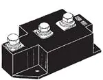
MDD312-14N1
Standard Rectifier Module
VRRM
= 2x 1400 V
I FAV
=
310 A
VF
=
1,03 V
Phase leg
Part number
MDD312-14N1
Backside: isolated
2
1
3
Features / Advantages:
Applications:
Package: Y1
● Package with DCB ceramic
● Improved temperature and power cycling
● Planar passivated chips
● Very low forward voltage drop
● Very low leakage current
● Diode for main rectification
● For single and three phase
bridge configurations
● Supplies for DC power equipment
● Input rectifiers for PWM inverter
● Battery DC power supplies
● Field supply for DC motors
● Isolation Voltage: 4800 V~
● Industry standard outline
● RoHS compliant
● Base plate: Copper
internally DCB isolated
● Advanced power cycling
Disclaimer Notice
Information furnished is believed to be accurate and reliable. However, users should independently
evaluate the suitability of and test each product selected for their own applications. Littelfuse products are not designed for,
and may not be used in, all applications. Read complete Disclaimer Notice at www.littelfuse.com/disclaimer-electronics.
IXYS reserves the right to change limits, conditions and dimensions.
© 2022 IXYS all rights reserved
Data according to IEC 60747and per semiconductor unless otherwise specified
20220914k
�MDD312-14N1
Ratings
Rectifier
Conditions
Symbol
VRSM
Definition
max. non-repetitive reverse blocking voltage
TVJ = 25°C
VRRM
max. repetitive reverse blocking voltage
TVJ = 25°C
1400
IR
reverse current
VR = 1400 V
TVJ = 25°C
500
µA
VR = 1400 V
TVJ = 150°C
30
mA
I F = 300 A
TVJ = 25°C
1,13
V
1,33
V
1,03
V
VF
forward voltage drop
min.
typ.
I F = 600 A
TVJ = 125 °C
I F = 300 A
I F = 600 A
I FAV
average forward current
TC = 100°C
I F(RMS)
RMS forward current
180° sine
VF0
threshold voltage
rF
slope resistance
R thJC
thermal resistance junction to case
R thCH
thermal resistance case to heatsink
Ptot
total power dissipation
I FSM
max. forward surge current
I²t
CJ
value for fusing
junction capacitance
IXYS reserves the right to change limits, conditions and dimensions.
© 2022 IXYS all rights reserved
V
1,29
V
T VJ = 150°C
310
A
520
A
TVJ = 150°C
0,80
V
0,6
mΩ
d = 0.5
for power loss calculation only
max. Unit
1500
V
0,12 K/W
K/W
0,04
TC = 25°C
1040
W
t = 10 ms; (50 Hz), sine
TVJ = 45°C
10,8
kA
t = 8,3 ms; (60 Hz), sine
VR = 0 V
11,7
kA
t = 10 ms; (50 Hz), sine
TVJ = 150°C
9,18
kA
t = 8,3 ms; (60 Hz), sine
VR = 0 V
9,92
kA
t = 10 ms; (50 Hz), sine
TVJ = 45°C
t = 8,3 ms; (60 Hz), sine
VR = 0 V
566,1 kA²s
t = 10 ms; (50 Hz), sine
TVJ = 150°C
421,4 kA²s
t = 8,3 ms; (60 Hz), sine
VR = 0 V
VR = 400 V; f = 1 MHz
TVJ = 25°C
583,2 kA²s
409,0 kA²s
381
Data according to IEC 60747and per semiconductor unless otherwise specified
pF
20220914k
�MDD312-14N1
Package
Ratings
Y1
Symbol
I RMS
Definition
Conditions
RMS current
per terminal
min.
typ.
max.
600
Unit
A
TVJ
virtual junction temperature
-40
150
°C
T op
operation temperature
-40
125
°C
Tstg
storage temperature
-40
125
°C
680
Weight
g
MD
mounting torque
4,5
7
Nm
MT
terminal torque
11
13
Nm
d Spp/App
terminal to terminal
creepage distance on surface | striking distance through air
terminal to backside
d Spb/Apb
VISOL
t = 1 second
isolation voltage
t = 1 minute
Production
Index (PI)
Date Code
(DC)
50/60 Hz, RMS; IISOL ≤ 1 mA
16,0
mm
16,0
mm
4800
V
4000
V
Circuit
yywwAA
Part Number
Lot.No: xxxxxx
Data Matrix: part no. (1-19), DC + PI (20-25), lot.no.# (26-31),
blank (32), serial no.# (33-36)
Ordering
Standard
Ordering Number
MDD312-14N1
Similar Part
MDD312-12N1
MDD312-16N1
MDD312-18N1
MDD312-20N1
Y1-CU
Y1-CU
Y1-CU
Y1-CU
MDD312-22N1
Y1-CU
Equivalent Circuits for Simulation
I
V0
R0
Marking on Product
MDD312-14N1
Package
Delivery Mode
Box
Code No.
463434
Voltage class
1200
1600
1800
2000
2200
* on die level
T VJ = 150 °C
Rectifier
V 0 max
threshold voltage
0,8
V
R0 max
slope resistance *
0,4
mΩ
IXYS reserves the right to change limits, conditions and dimensions.
© 2022 IXYS all rights reserved
Quantity
3
Data according to IEC 60747and per semiconductor unless otherwise specified
20220914k
�MDD312-14N1
Outlines Y1
43
10
32 +0
-1,9
52 +0
-1,4
49
2
15 ±1
3x M8
35
28.5
1
2
38
50
22.5
45 67
18
20
3
6.2
80
92
115
2
IXYS reserves the right to change limits, conditions and dimensions.
© 2022 IXYS all rights reserved
1
3
Data according to IEC 60747and per semiconductor unless otherwise specified
20220914k
�MDD312-14N1
Rectifier
106
10000
DC
180 ° sin
120 °
60 °
30 °
500
50 Hz
80 % VRRM
TVJ = 45°C
TVJ = 150°C
8000
IFSM
VR = 0 V
400
IFAVM
I2t
6000
300
TVJ = 45°C
2
[A]
[A s]
[A]
200
TVJ = 150°C
4000
100
105
2000
0.01
0.1
1
0
1
10
t [s]
0
25
50
t [ms]
Fig. 2 I2t versus time (1-10 ms)
Fig. 1 Surge overload current
IFSM: Crest value, t: duration
75
Fig. 3 Maximum forward current
at case temperature
600
600
TVJ = 125°C
VR = 600 V
R thKA K/W
0.06
0.1
0.2
0.3
0.4
0.6
0.8
500
400
Ptot
500
400
IRM
300
300
DC
180 ° sin
120 °
60 °
30 °
[W]
200
[A]
IF = 400 A
200
100
100
0
0
0
100
200
300
400
500
0
25
IFAVM [A]
50
75
100
125
150
0
50
TA [°C]
100
150
200
di F /dt [A/µs]
Fig. 5 Typ. peak reverse current
Fig. 4 Power dissipation vs. forward current & ambient temperature (per diode)
25
1750
TVJ = 125°C
VR = 600 V
R thKA K/W
1500
0.04
0.06
0.08
0.12
0.2
0.3
0.5
1250
Ptot
100 125 150
TC [°C]
R
L
1000
20
trr
15
[W]
[µs]
750
IF = 400 A
10
Circuit
B2U
2 x MDD312
500
5
250
0
0
0
100 200 300 400 500 600
0
IdAVM [A]
25
50
75
100
125
150
TA [°C]
Fig. 6 Single phase rectifier bridge: Power dissipation vs. direct output current
and ambient temperature R = resistive load, L = inductive load
IXYS reserves the right to change limits, conditions and dimensions.
© 2022 IXYS all rights reserved
0
50
100
150
200
diF /dt [A/µs]
Fig. 7 Typ. recovery time trr
versus -diF /dt
Data according to IEC 60747and per semiconductor unless otherwise specified
20220914k
�MDD312-14N1
Rectifier
3000
R thKA K/W
0.03
0.06
0.1
0.15
0.2
0.3
0.4
2500
2000
Ptot
1500
[W]
Circuit
B6U
3 x M DD 312
1000
500
0
0
200
400
600
800
0
25
50
75
100
125
150
TA [°C]
IFAVM [A]
Fig. 8 Three phase rectifier bridge: Power dissipation vs. direct output current & ambient temperature
0.20
RthJC for various conduction angles d:
RthJC [K/W]
d
0.120
DC
180°
0.128
0.135
120°
0.153
60°
30°
0.185
0.15
ZthJC
0.10
30°
60°
120°
180°
DC
[K/W]
0.05
0.00
10-3
10-2
10-1
100
Constants for ZthJC calculation:
101
102
i
1
2
3
4
Rthi (K/W)
0.0058
0.0310
0.0720
0.0112
ti (s)
0.00054
0.09800
0.54000
12.0000
t [s]
Fig. 9 Transient thermal impedance junction to case (per diode)
0.25
RthJK for various conduction angles d:
RthJK [K/W]
d
0.160
DC
180°
0.168
0.175
120°
0.193
60°
30°
0.225
0.20
ZthJK
0.15
[K/W]
0.10
30°
60°
120°
180°
DC
0.05
0.00
10-3
10-2
10-1
100
101
t [s]
Constants for ZthJK calculation:
102
i
1
2
3
4
5
Rthi (K/W)
0.0058
0.0310
0.0720
0.0112
0.0400
ti (s)
0.00054
0.09800
0.54000
12.0000
12.0000
Fig. 10 Transient thermal impedance junction to heatsink (per diode)
IXYS reserves the right to change limits, conditions and dimensions.
© 2022 IXYS all rights reserved
Data according to IEC 60747and per semiconductor unless otherwise specified
20220914k
�


 工商网监
湘ICP备2023018690号
工商网监
湘ICP备2023018690号
