VUB120-16NOX
3~
Rectifier
Standard Rectifier Module
Brake
Chopper
VRRM = 1600 V VCES = 1200 V
I DAV =
180 A I C25
= 180 A
I FSM = 1100 A VCE(sat) =
1.7 V
3~ Rectifier Bridge + Brake Unit
Part number
VUB120-16NOX
Backside: isolated
M1/O1
S1
U1/
W1
~A6
~E6
~K6
M10/O10
W U S/T
10 10 10
Features / Advantages:
Applications:
Package: V2-Pack
● Package with DCB ceramic base plate
● Improved temperature and power cycling
● Planar passivated chips
● Very low forward voltage drop
● Very low leakage current
● X2PT - 2nd generation Xtreme light Punch Through
● Rugged X2PT design results in:
- short circuit rated for 10 µsec.
- very low gate charge
- low EMI
- square RBSOA @ 2x Ic
● Thin wafer technology combined with X2PT design
results in a competitive low VCE(sat) and low
thermal resistance
● 3~ Rectifier with brake unit
for drive inverters
● Isolation Voltage: 3600 V~
● Industry standard outline
● RoHS compliant
● Soldering pins for PCB mounting
● Height: 17 mm
● Base plate: DCB ceramic
● Reduced weight
● Advanced power cycling
Disclaimer Notice
Information furnished is believed to be accurate and reliable. However, users should independently
evaluate the suitability of and test each product selected for their own applications. Littelfuse products are not designed for,
and may not be used in, all applications. Read complete Disclaimer Notice at www.littelfuse.com/disclaimer-electronics.
IXYS reserves the right to change limits, conditions and dimensions.
© 2019 IXYS all rights reserved
Data according to IEC 60747and per semiconductor unless otherwise specified
20191220h
�VUB120-16NOX
Ratings
Rectifier
Conditions
Symbol
VRSM
Definition
max. non-repetitive reverse blocking voltage
TVJ = 25°C
VRRM
max. repetitive reverse blocking voltage
TVJ = 25°C
1600
IR
reverse current
VF
forward voltage drop
min.
typ.
VR = 1600 V
TVJ = 25°C
100
µA
TVJ = 125°C
2
mA
IF =
TVJ = 25°C
1.16
V
1.55
V
1.09
V
IF =
60 A
TVJ = 125 °C
60 A
I F = 180 A
bridge output current
VF0
threshold voltage
rF
slope resistance
R thJC
thermal resistance junction to case
TC = 90 °C
rectangular
R thCH
thermal resistance case to heatsink
total power dissipation
I FSM
max. forward surge current
I²t
CJ
value for fusing
junction capacitance
IXYS reserves the right to change limits, conditions and dimensions.
© 2019 IXYS all rights reserved
1.59
V
T VJ = 150 °C
180
A
TVJ = 150 °C
0.81
V
4.4
mΩ
d=⅓
for power loss calculation only
Ptot
V
VR = 1600 V
I F = 180 A
I DAV
max. Unit
1700
V
0.6 K/W
0.2
K/W
TC = 25°C
205
W
t = 10 ms; (50 Hz), sine
TVJ = 45°C
1.10
kA
t = 8,3 ms; (60 Hz), sine
VR = 0 V
1.19
kA
t = 10 ms; (50 Hz), sine
TVJ = 150 °C
935
A
t = 8,3 ms; (60 Hz), sine
VR = 0 V
1.01
kA
t = 10 ms; (50 Hz), sine
TVJ = 45°C
6.05 kA²s
t = 8,3 ms; (60 Hz), sine
VR = 0 V
5.89 kA²s
t = 10 ms; (50 Hz), sine
TVJ = 150 °C
4.37 kA²s
t = 8,3 ms; (60 Hz), sine
VR = 0 V
VR = 400 V; f = 1 MHz
TVJ = 25°C
4.25 kA²s
37
Data according to IEC 60747and per semiconductor unless otherwise specified
pF
20191220h
�VUB120-16NOX
Ratings
Brake IGBT + Diode
Symbol
VCES
Definition
Conditions
min.
VGES
max. DC gate voltage
±20
V
VGEM
max. transient gate emitter voltage
±30
V
I C25
collector current
TC = 25°C
180
A
TC = 80 °C
140
A
500
W
2.1
V
TVJ =
collector emitter voltage
I C80
Ptot
total power dissipation
VCE(sat)
collector emitter saturation voltage
VGE(th)
gate emitter threshold voltage
I C = 4 mA; VGE = V CE
TVJ = 25°C
I CES
collector emitter leakage current
VCE = VCES ; V GE = 0 V
TVJ = 25°C
I GES
gate emitter leakage current
VGE = ±20 V
Q G(on)
total gate charge
VCE = 600 V; VGE = 15 V; I C =100 A
t d(on)
turn-on delay time
TC = 25°C
I C = 100 A; V GE = 15 V
TVJ = 25°C
1.7
TVJ = 125°C
1.9
TVJ = 125°C
tr
current rise time
t d(off)
turn-off delay time
tf
current fall time
Eon
turn-on energy per pulse
Eoff
turn-off energy per pulse
RBSOA
reverse bias safe operating area
typ.
25°C
inductive load
6.8
TVJ = 125°C
VGE = ±15 V; R G = 6.8 Ω
SCSOA
short circuit safe operating area
t SC
short circuit duration
VCEK = 1200 V
VCE = 720 V; VGE = ±15
I SC
short circuit current
RG = 6.8 Ω; non-repetitive
R thJC
thermal resistance junction to case
R thCH
thermal resistance case to heatsink
7.5
V
0.1
mA
0.1
mA
nA
340
nC
230
ns
70
ns
380
ns
230
ns
12.5
mJ
11.5
mJ
TVJ = 125°C
VCEK = 1200 V
I CM
V
500
VCE = 600 V; IC = 100 A
VGE = ±15 V; R G = 6.8 Ω
6
max. Unit
1200
V
TVJ = 125°C
300
A
10
µs
A
450
0.25 K/W
K/W
0.10
Brake Diode
VRRM
max. repetitive reverse voltage
TVJ = 25°C
1200
V
I F25
forward current
TC = 25°C
48
A
TC = 80 °C
32
A
TVJ = 25°C
2.75
V
TVJ = 25°C
0.25
mA
TVJ = 125°C
1
mA
I F80
VF
forward voltage
I F = 30 A
IR
reverse current
VR = VRRM
Q rr
reverse recovery charge
VR =
I RM
max. reverse recovery current
-di F /dt = 1000 A/µs
trr
reverse recovery time
IF =
E rec
reverse recovery energy
R thJC
thermal resistance junction to case
RthCH
thermal resistance case to heatsink
TVJ = 125°C
IXYS reserves the right to change limits, conditions and dimensions.
© 2019 IXYS all rights reserved
600 V
30 A; VGE = 0 V
TVJ = 125°C
1.60
V
5.2
µC
50
A
300
ns
1.9
mJ
0.9 K/W
0.3
Data according to IEC 60747and per semiconductor unless otherwise specified
K/W
20191220h
�VUB120-16NOX
Package
Ratings
V2-Pack
Symbol
I RMS
Definition
Conditions
RMS current
per terminal
min.
TVJ
virtual junction temperature
T op
operation temperature
Tstg
storage temperature
-40
max.
100
Unit
A
-40
150
°C
-40
125
°C
125
°C
76
Weight
MD
2
mounting torque
d Spp/App
creepage distance on surface | striking distance through air
d Spb/Apb
VISOL
typ.
t = 1 minute
2.5
Nm
terminal to terminal
6.0
mm
terminal to backside
12.0
mm
3600
V
3000
V
t = 1 second
isolation voltage
g
50/60 Hz, RMS; IISOL ≤ 1 mA
Data Matrix: Typ (1-19), DC+Prod.Index (20-25), FKT# (26-31)
leer (33), lfd.# (33-36)
yywwAA
Part Number
Lot.No: xxxxxx
UL Date code
Prod. Index
Ordering
Standard
Ordering Number
VUB120-16NOX
Similar Part
VUB120-16NOXT
Equivalent Circuits for Simulation
I
V0
R0
Marking on Product
VUB120-16NOX
Package
V2-Pack
* on die level
Rectifier
Brake
Diode
V 0 max
threshold voltage
0.81
1.31
R0 max
slope resistance *
3.2
8
IXYS reserves the right to change limits, conditions and dimensions.
© 2019 IXYS all rights reserved
Delivery Mode
Box
Quantity
6
Code No.
520475
Voltage class
1600
T VJ = 150°C
V
mΩ
Data according to IEC 60747and per semiconductor unless otherwise specified
20191220h
�VUB120-16NOX
Outlines V2-Pack
Marking
Remarks:
EJOT PT® self-tapping screws of the dimension K25 are
recommended for the mechanical connection between module
and PCB. Choose the right length according to your board
thickness at a maximum depth of 6 mm of the module holes.
The recommended mounting torque is 1.5 Nm.
M1/O1
S1
U1/
W1
~A6
~E6
~K6
M10/O10
W U S/T
10 10 10
IXYS reserves the right to change limits, conditions and dimensions.
© 2019 IXYS all rights reserved
Data according to IEC 60747and per semiconductor unless otherwise specified
20191220h
�VUB120-16NOX
Rectifier
200
10 4
900
TVJ = 125°C
TVJ = 25°C
800
IF
IFSM
TVJ= 45°C
TVJ = 45°C
150
2
700
It
600
[A s]
TVJ= 150°C
100
[A]
[A]
2
50
TVJ = 150°C
500
0
0.0
50Hz, 80% VRRM
0.5
1.0
1.5
400
0.001
2.0
0.01
VF [V]
0.1
10 3
1
1
2
t [s]
Fig. 1 Forward current vs.
voltage drop per diode
3
4
5 6 7 8 910
t [ms]
2
Fig. 2 Surge overload current
vs. time per diode
Fig. 3 I t vs. time per diode
140
RthA:
0.1 K/W
0.3 K/W
0.6 K/W
1.0 K/W
1.5 K/W
2.5 K/W
DC =
1
0.5
0.4
0.33
0.17
0.08
80
60
Ptot
40
DC =
1
0.5
0.4
0.33
0.17
0.08
120
100
IdAV 80
[A] 60
[W]
40
20
20
0
0
0
10
20
30
40
50
60
70
0
20
40
IF(AV)M [A]
60
80 100 120 140 160
0
25
50
Tamb [°C]
75
100 125 150
TC [°C]
Fig. 4 Power dissipation vs. forward current
and ambient temperature per diode
Fig. 5 Max. forward current vs.
case temperature per diode
0.6
0.5
Constants for ZthJC calculation:
0.4
ZthJC
0.3
[K/W]
0.2
0.1
0.0
1
10
100
1000
i
Rth (K/W)
ti (s)
1
0.040
0.004
2
0.003
0.010
3
0.140
0.030
4
0.120
0.300
5
0.197
0.080
10000
t [s]
Fig. 6 Transient thermal impedance junction to case vs. time per diode
IXYS reserves the right to change limits, conditions and dimensions.
© 2019 IXYS all rights reserved
Data according to IEC 60747and per semiconductor unless otherwise specified
20191220h
�VUB120-16NOX
Brake IGBT + Diode
200
200
150
13 V
VCE = 20 V
150
150
25°C
IC
200
VGE = 19 V
17 V
15 V
IC
125°C
100
11 V
TVJ = 150°C
IC
100
100
[A]
[A]
[A]
125°C
50
50
50
25°C
9V
0
0.0
0
0
0.5
1.0
1.5
2.0
2.5
3.0
0
1
VCE [V]
400
RG = 6.8 Ohm
VCE = 600 V
VGE = ±15 V
TVJ = 125°C
30
3
6
4
7
RG = 6.8 Ohm
VCE = 600 V
VGE = ±15 V
TVJ = 125°C
40
300
td(on)
Eon
tr
20
200
[mJ]
[ns]
10 11 12
13
Eoff
60
500
50
400
t
t d(off)
30
40
300
[mJ]
[ns]
tf
20
200
IF
30
[A]
125°C
20
tr
10
9
Fig. 3 Typ. transfer charact.
IGBT
Fig.2 Typ. output characteristics
IGBT
50
8
VGE [V]
VCE [V]
Fig.1 Output characteristics IGBT
40
2
100
10
100
10
25°C
Eon
0
0
0
50
100
150
0
200
0
IC [A]
Fig. 4 Typ. turn-on energy & switch.
times vs. collector current
8
80
RG = 6.8 Ohm
VR = 600 V
TVJ = 125°C
I rr
6
Eoff
Erec
Irr
4
40
[A]
[mJ]
100
150
200
IC [A]
Fig. 5 Typ. turn-off energy & switch.
times vs. collector current
2.5
2.0
60
Erec
0
10
20
30
40
50
0
60
1.5
2.0
2.5
1
100
Erec
IGBT
1.5
75
[mJ]
ZthJC
Irr
1.0
50
0.1
[K/W]
[A]
20
Erec
1.0
Diode
0.5
0
0.5
VF [V]
Fig. 6 Typ. forward characteristics
Diode
125
TVJ = 125°C
VR = 600 V
IF = 30 A
Irr
2
0
0.0
0
50
25
0.0
4
8
12
16
20
0
24
0.01
0.001
IGBT
Ri
ti
0.050 0.0010
0.035 0.0100
0.120 0.0300
0.045 0.0800
0.01
Diode
Ri
ti
0.365 0.0050
0.180 0.0003
0.255 0.0397
0.100 0.1000
0.1
1
IF [A]
RG [Ohm]
t [s]
Fig. 7 Typ. reverse recovery
characteristics Diode
Fig. 8 Typ. reverse recovery
characteristics Diode
Fig. 9 Transient thermal
resistance junction to case
IXYS reserves the right to change limits, conditions and dimensions.
© 2019 IXYS all rights reserved
Data according to IEC 60747and per semiconductor unless otherwise specified
20191220h
�
很抱歉,暂时无法提供与“VUB120-16NOXT”相匹配的价格&库存,您可以联系我们找货
免费人工找货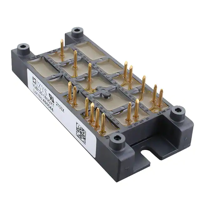


 工商网监
湘ICP备2023018690号
工商网监
湘ICP备2023018690号
