JIANGSU CHANGJING ELECTRONICS TECHNOLOGY CO., LTD
SOD-123 Plastic-Encapsulate Diodes
BZT52C2V4-BZT52C43 ZENER DIODE
SOD-123
FEATURES:
z
Planar Die Construction
z
500mW Power Dissipation on Ceramic PCB
z
General Purpose, Medium Current
z
Ideally Suited for Automated Assembly Processes
z
Available in Lead Free Version
Maximum Ratings(Ta=25℃ unless otherwise specified)
Characteristic
Forward Voltage (Note 2)
@ IF = 10mA
Power Dissipation(Note 1)
Thermal Resistance from Junction to Ambient(Note 1)
Operation Junction and Storage Temperature Range
www.jscj-elec.com
1
Symbol
Value
Unit
VF
0.9
V
PD
500
mW
RθJA
TJ,TSTG
250
-55~+150
℃ /W
℃
Rev. - 2.0
�ELECTRICAL CHARACTERISTICS
Ta=25℃ unless otherwise specified
Type
Type
Number
Code
Zener Voltage Range (Note 2)
Maximum
Typical
Maximum Zener Impedance
Reverse
Temperature
(Note 3)
Current
Coefficent
(Note 2)
IZT
VZ@IZT
Nom(V)
Min(V)
Max(V)
mA
ZZT@IZT
ZZK@IZK
Ω
@IZTC
Test
Current
IZTC
mV/°C
IZK
IR
VR
mA
uA
V
Min
Max
mA
BZT52C2V4
WX
2.4
2.20
2.60
5
100
600
1.0
50
1.0
-3.5
0
5
BZT52C2V7
W1
2.7
2.5
2.9
5
100
600
1.0
20
1.0
-3.5
0
5
BZT52C3V0
W2
3.0
2.8
3.2
5
95
600
1.0
10
1.0
-3.5
0
5
BZT52C3V3
W3
3.3
3.1
3.5
5
95
600
1.0
5
1.0
-3.5
0
5
BZT52C3V6
W4
3.6
3.4
3.8
5
90
600
1.0
5
1.0
-3.5
0
5
BZT52C3V9
W5
3.9
3.7
4.1
5
90
600
1.0
3
1.0
-3.5
0
5
BZT52C4V3
W6
4.3
4.0
4.6
5
90
600
1.0
3
1.0
-3.5
0
5
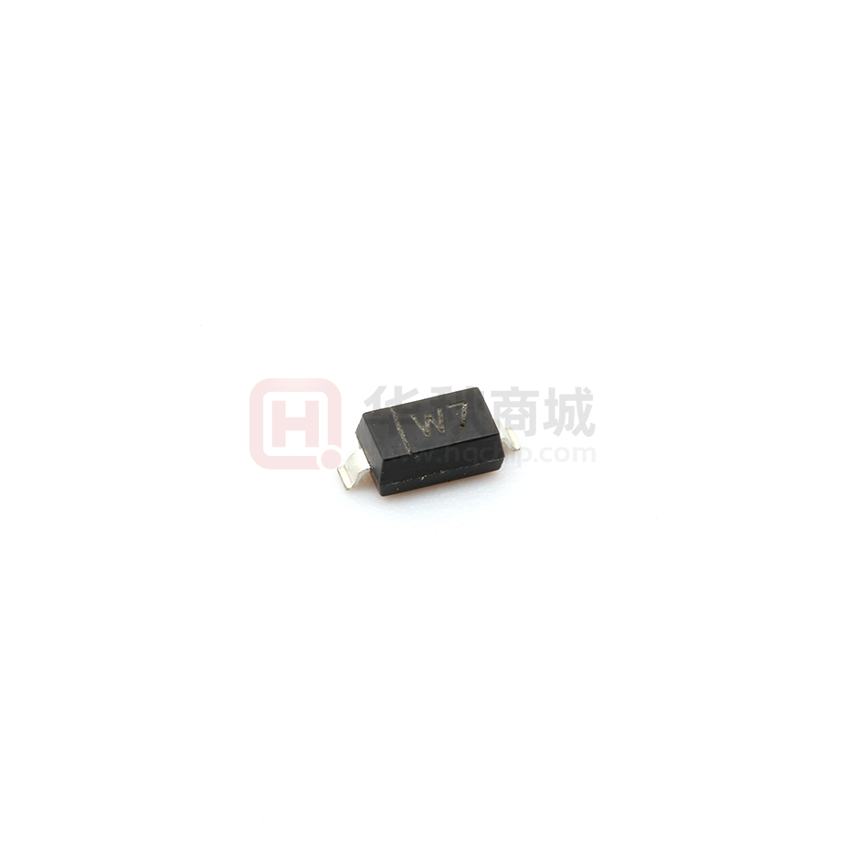
BZT52C4V7
W7
4.7
4.4
5.0
5
80
500
1.0
3
2.0
-3.5
0.2
5
BZT52C5V1
W8
5.1
4.8
5.4
5
60
480
1.0
2
2.0
-2.7
1.2
5
BZT52C5V6
W9
5.6
5.2
6.0
5
40
400
1.0
1
2.0
-2.0
2.5
5
BZT52C6V2
WA
6.2
5.8
6.6
5
10
150
1.0
3
4.0
0.4
3.7
5
BZT52C6V8
WB
6.8
6.4
7.2
5
15
80
1.0
2
4.0
1.2
4.5
5
BZT52C7V5
WC
7.5
7.0
7.9
5
15
80
1.0
1
5.0
2.5
5.3
5
BZT52C8V2
WD
8.2
7.7
8.7
5
15
80
1.0
0.7
5.0
3.2
6.2
5
BZT52C9V1
WE
9.1
8.5
9.6
5
15
100
1.0
0.5
6.0
3.8
7.0
5
BZT52C10
WF
10
9.4
10.6
5
20
150
1.0
0.2
7.0
4.5
8.0
5
BZT52C11
WG
11
10.4
11.6
5
20
150
1.0
0.1
8.0
5.4
9.0
5
BZT52C12
WH
12
11.4
12.7
5
25
150
1.0
0.1
8.0
6.0
10.0
5
BZT52C13
WI
13
12.4
14.1
5
30
170
1.0
0.1
8.0
7.0
11.0
5
BZT52C15
WJ
15
13.8
15.6
5
30
200
1.0
0.1
10.5
9.2
13.0
5
BZT52C16
WK
16
15.3
17.1
5
40
200
1.0
0.1
11.2
10.4
14.0
5
BZT52C18
WL
18
16.8
19.1
5
45
225
1.0
0.1
12.6
12.4
16.0
5
BZT52C20
WM
20
18.8
21.2
5
55
225
1.0
0.1
14.0
14.4
18.0
5
BZT52C22
WN
22
20.8
23.3
5
55
250
1.0
0.1
15.4
16.4
20.0
5
BZT52C24
WO
24
22.8
25.6
5
70
250
1.0
0.1
16.8
18.4
22.0
5
BZT52C27
WP
27
25.1
28.9
2
80
300
0.5
0.1
18.9
21.4
25.3
2
BZT52C30
WQ
30
28.0
32.0
2
80
300
0.5
0.1
21.0
24.4
29.4
2
BZT52C33
WR
33
31.0
35.0
2
80
325
0.5
0.1
23.1
27.4
33.4
2
BZT52C36
WS
36
34.0
38.0
2
90
350
0.5
0.1
25.2
30.4
37.4
2
BZT52C39
WT
39
37.0
41.0
2
130
350
0.5
0.1
27.3
33.4
41.2
2
BZT52C43
WU
43
40.0
46.0
5
100
700
1.0
0.1
32
10.0
12.0
5
Notes: 1.The value of RθJA is measured with the device mounted on 1 in 2 FR-4 board with 2oz. Copper, in a still air
environment with Ta=25 ℃.
2. Short duration test pulse used to minimize self-heating effect
3. f=1kHZ
www.jscj-elec.com
2
Rev. - 2.0
�Typical Characteristics
100
Ta =25℃
PD =500mW
Pulsed
1
0.5
1
2
3
4
5
6
7
8
9
10
11
10
15
25
30
43
39
36
40
45
50
Typical Leakage Current
100
Pulsed
FOR BZT52CXXX SERIES
10
IR, LEAKAGE CURRENT (uA)
30
25
20
VZ @ IZT
15
10
5
1
0.1
0.01
Ta=100℃
1E-3
0
Ta=25℃
0
4
8
12
16
20
24
28
32
36
40
1E-4
44
0
5
VZ, NOMINAL ZENER VOLTAGE (V)
10
15
20
25
30
35
40
45
VZ, NOMINAL ZENER VOLTAGE (V)
Effect of Zener Voltage on Zener Impedance
Typical Capacitance
1000
1000
Ta=25℃
Ta=25℃
f=1MHz
ZZT, DYNAMIC IMPEDANCE(Ω)
100
1V BIAS
BIAS AT
50% OF VZ NOM
10
1
10
IZ(AC)=0.1IZ(DC)
IZ=1mA
0V BIAS
C, CAPACITANCE (pF)
35
TYPICAL Ta VALUES
35
1
33
27
30
22
20
VZ, ZENER VOLTAGE (V)
Temperature Coefficients
40
θVZ, TEMPERATURE COEFFICIENT (mV/℃)
24
1
VZ, ZENER VOLTAGE (V)
-5
20
18
10
16
10
9.1
8.2
7.5
6.2
6.8
5.6
4.7
2.4
5.1
10
PD =500mW
11
12
13
IZ, ZENER CURRENT (mA)
Pulsed
15
Ta =25℃
IZ, ZENER CURRENT (mA)
Zener Characteristics(11 V to 43 V)
Zener Characteristics(VZ Up to 10 V)
100
100
IZ=5mA
10
1
100
VZ, NOMINAL ZENER VOLTAGE (V)
f=1kHz
1
10
100
VZ, NOMINAL ZENER VOLTAGE (V)
Power Derating Curve
800
POWER DISSIPATION
PD
(mW)
700
600
500
400
300
200
100
0
0
25
50
75
AMBIENT TEMPERATURE
www.jscj-elec.com
100
Ta
125
150
(℃ )
3
Rev. - 2.0
�SOD-123 Package Outline Dimensions
Dimensions In Millimeters
Min
Max
1.050
1.250
0.000
0.100
1.050
1.150
0.450
0.650
0.080
0.150
1.500
1.700
2.600
2.800
3.550
3.850
0.500 REF
0.250
0.450
0°
8°
Symbol
A
A1
A2
b
c
D
E
E1
L
L1
θ
Dimensions In Inches
Min
Max
0.049
0.041
0.000
0.004
0.041
0.045
0.018
0.026
0.003
0.006
0.059
0.067
0.102
0.110
0.140
0.152
0.020 REF
0.010
0.018
0°
8°
SOD-123 Suggested Pad Layout
NOTICE
JSCJ reserves the right to make modifications,enhancements,improvements,corrections or other
changes without further notice to any product herein. JSCJ does not assume any liability arising
out of the application or use of any product described herein.
www.jscj-elec.com
4
Rev. - 2.0
�SOD-123 Tape and Reel
www.jscj-elec.com
5
Rev. - 2.0
�
很抱歉,暂时无法提供与“BZT52C4V7”相匹配的价格&库存,您可以联系我们找货
免费人工找货