JIANGSU CHANGJIANG ELECTRONICS TECHNOLOGY CO., LTD
SOT-23 Plastic-Encapsulate MOSFETS
CJ2303 P-Channel 30-V(D-S) MOSFET
V(BR)DSS
ID
RDS(on)MAX
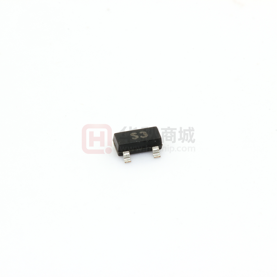
SOT-23
190mΩ@-10V
-30 V
-1.9A
330mΩ@-4.5V
1. GATE
2. SOURCE
3. DRAIN
FEATURE
z TrenchFET Power MOSFET
APPLICATION
z
Load Switch for Portable Devices
DC/DC Converter
z
MARKING
Equivalent Circuit
Maximum ratings (Ta=25℃ unless otherwise noted)
Parameter
Symbol
Value
Unit
Drain-Source Voltage
VDS
-30
Gate-Source Voltage
VGS
±20
Continuous Drain Current
ID
-1.9
Continuous Source-Drain Diode Current
IS
-0.83
Maximum Power Dissipation
PD
0.35
W
RθJA
357
℃/W
Thermal Resistance from Junction to Ambient(t≤5s)
Junction Temperature
TJ
150
Storage Temperature
TSTG
-50 ~+150
www.cj-elec.com
1
V
A
℃
D,Aug,2015
�MOSFET ELECTRICAL CHARACTERISTICS
Ta =25 ℃ unless otherwise specified
Parameter
Symbol
Test Condition
Min
V(BR)DSS
VGS = 0V, ID =-250µA
-30
VGS(th)
VDS =VGS, ID =-250µA
-1
Gate-Source Leakage
IGSS
VDS =0V, VGS =±20V
±100
nA
Zero Gate Voltage Drain Current
IDSS
VDS =-30V, VGS =0V
-1
µA
Typ
Max
-1.6
-3
Units
Static
Drain-Source Breakdown Voltage
Gate-Source Threshold Voltage
a
Drain-Source On-State Resistance
Forward Transconductance
RDS(on)
a
gfs
VGS =-10V, ID =-1.9A
0.075
0.190
VGS =-4.5V, ID =-1.4A
0.115
0.330
VDS =-5V, ID =-1.9A
1
V
Ω
S
b
Dynamic
Input Capacitance
Ciss
Output Capacitance
Coss
Reverse Transfer Capacitance
Crss
Total Gate Charge
Qg
Gate-Source Charge
Qgs
Gate-Drain Charge
Qgd
Gate Resistance
Rg
Turn-On Delay Time
td(on)
Rise Time
tr
Turn-Off Delay Time
td(off)
Fall Time
tf
Turn-On Delay Time
td(on)
Rise Time
tr
Turn-Off Delay Time
td(off)
Fall Time
tf
155
VDS =-15V,VGS =0V,f =1MHz
pF
35
25
VDS =-15V,VGS =-10V,ID =-1.9A
VDS =-15V,VGS =-4.5V,ID=-1.9A
4
8
2
4
0.6
nC
1
f =1MHz
VDD=-15V,
RL=10Ω, ID =-1.5A,
VGEN=-10V,Rg=1Ω
VDD=-15V,
RL=10Ω, ID =-1.5A,
VGEN=-4.5V,Rg=1Ω
1.7
8.5
17
4
8
11
18
11
18
8
16
36
44
37
45
12
18
9
14
Ω
ns
Drain-source Body diode characteristics
Continuous Source-Drain Diode
Current
Pulse Diode Forward Current
Body Diode Voltage
a
IS
-1.75
TC=25℃
-10
ISM
VSD
A
IS=-1.5A
-0.8
-1.2
V
Notes :
a. Pulse Test : Pulse Width ≤300µs, Duty Cycle ≤2%.
b. Guaranteed by design, not subject to production testing.
www.cj-elec.com
2
D,Aug,2015
�Typical Characteristics
Output Characteristics
Transfer Characteristics
-20
-12
VDS=-3.0V
Ta=25℃
-18
Pulsed
VGS=-6V
Pulsed
-10
ID
VGS=-4.5V
-10
VGS=-4V
-8
VGS=-3.5V
-6
VGS=-3V
-4
Ta=25℃
Ta=100℃
-3
-5
(A)
VGS=-5V
DRAIN CURRENT
(A)
-12
DRAIN CURRENT
-14
ID
-16
-8
-6
-4
-2
-2
-0
-0
-0
-1
-2
-3
DRAIN TO SOURCE VOLTAGE
RDS(ON)
——
VDS
-4
-0
ID
RDS(ON)
Pulsed
(mΩ)
120
RDS(ON)
VGS=-4.5V
100
ON-RESISTANCE
(mΩ)
——
-7
VGS
-8
-9
-10
-9
-10
(V)
VGS
700
130
RDS(ON)
-6
Ta=25℃
140
ON-RESISTANCE
-4
800
150
90
-2
GATE TO SOURCE VOLTAGE
160
110
-1
(V)
80
70
VGS=-10V
60
50
40
600
ID=-2A
500
400
300
Ta=100℃
200
Pulsed
Ta=25℃
100
Pulsed
30
20
0
-0
-1
-2
-3
DRAIN CURRENT
IS
——
ID
-4
-5
-0
-1
-2
-3
-4
-5
-6
GATE TO SOURCE VOLTAGE
(A)
VSD
-7
VGS
-8
(V)
Threshold Voltage
-5
-1.8
(V)
VTH
-1
Ta=100℃
Pulsed
-0.1
THRESHOLD VOLTAGE
SOURCE CURRENT
IS
(A)
-1.7
Ta=25℃
Pulsed
-1.6
ID=-250uA
-1.5
-1.4
-1.3
-0.01
-0.0
-0.4
-0.8
SOURCE TO DRAIN VOLTAGE
-1.2
VSD
(V)
-1.6
-1.2
25
50
75
JUNCTION TEMPERATURE
100
TJ
125
( ℃)
�������������
��������������������������������������������������������������������3��������������������������������������������������������������������������� D,Aug,2015
�SOT-23 Package Outline Dimensions
Symbol
A
A1
A2
b
c
D
E
E1
e
e1
L
L1
θ
Dimensions In Millimeters
Min
Max
0.900
1.150
0.000
0.100
0.900
1.050
0.300
0.500
0.080
0.150
2.800
3.000
1.200
1.400
2.250
2.550
0.950 TYP
1.800
2.000
0.550 REF
0.300
0.500
0°
8°
Dimensions In Inches
Min
Max
0.035
0.045
0.000
0.004
0.035
0.041
0.012
0.020
0.003
0.006
0.110
0.118
0.047
0.055
0.089
0.100
0.037 TYP
0.071
0.079
0.022 REF
0.012
0.020
0°
8°
SOT-23 Suggested Pad Layout
www.cj-elec.com
4
D,Aug,2015
�SOT-23 Tape and Reel
www.cj-elec.com
5
D,Aug,2015
�
很抱歉,暂时无法提供与“CJ2303”相匹配的价格&库存,您可以联系我们找货
免费人工找货- 国内价格
- 10+0.23671
- 100+0.23316
- 600+0.16018
- 1200+0.15858
- 3000+0.15541