JIANGSU CHANGJIANG ELECTRONICS TECHNOLOGY CO., LTD
SOT-23 Plastic-Encapsulate MOSFETS
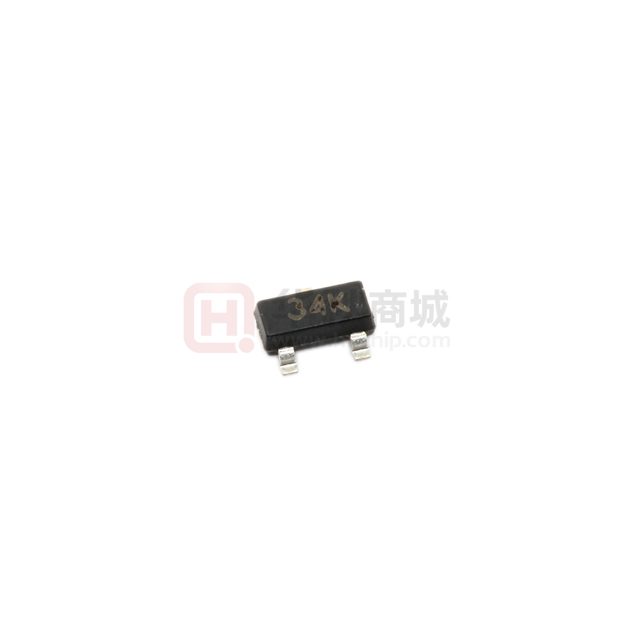
CJ3134K
N-Channel MOSFET
V(BR)DSS
ID
RDS(on)MAX
20 V
SOT-23
380mΩ@ 4.5V
450mΩ@ 2.5V
0.75A
800mΩ@1.8V
1. GATE
2. SOURCE
3. DRAIN
FEATURES
z Lead Free Product is Acquired
z Surface Mount Package
z N-Channel Switch with Low RDS(on)
z Operated at Low Logic Level Gate Drive
MARKING
APPLICATION
z Load/Power Switching
z Interfacing Switching
z Battery Management for Ultra Small Portable Electronics
z Logic Level Shift
Equivalent Circuit
Maximum ratings (Ta=25℃ unless otherwise noted)
Symbol
Value
Drain-Source Voltage
VDS
20
V
Typical Gate-Source Voltage
VGS
±12
V
Continuous Drain Current (note 1)
ID
0.75
A
Pulsed Drain Current
IDM
1.8
A
PD
350
mW
RθJA
357
℃/W
Junction Temperature
TJ
150
℃
Storage Temperature
TSTG
-55~+150
℃
TL
260
℃
Parameter
(tp=10μs)
Power Dissipation (note 1)
Thermal Resistance from Junction to Ambient (note 1)
Lead Temperature for Soldering Purposes(1/8” duration for 10 s)
Unit
B Dec,2013
www.cj-elec.com
1
F,Aug,2015
�MOSFET ELECTRICAL CHARACTERISTICS
Ta =25 ℃ unless otherwise specified
Parameter
Symbol
Test Condition
Min
Typ
Max
Unit
STATIC CHARACTERISTICS
Drain-source breakdown voltage
V (BR)DSS
VGS = 0V, ID =250µA
Zero gate voltage drain current
IDSS
VDS =20V,VGS = 0V
Gate-body leakage current
IGSS
VGS =±10V, VDS = 0V
VGS(th)
VDS =VGS, ID =250µA
Gate threshold voltage (note 2)
Drain-source on-resistance (note 2)
RDS(on)
20
V
1
µA
±20
µA
0.54
1.1
V
VGS =4.5V, ID =0.65A
270
380
mΩ
VGS =2.5V, ID =0.55A
320
450
mΩ
VGS =1.8V, ID =0.45A
390
800
mΩ
1.6
Forward transconductance (note 2)
gFS
VDS =10V, ID =0.8A
Diode forward voltage
VSD
IS=0.15A, VGS = 0V
0.35
S
1.2
V
79
120
pF
13
20
pF
15
pF
DYNAMIC CHARACTERISTICS (note 4)
Input capacitance
Ciss
Output capacitance
Coss
Reverse transfer capacitance
Crss
9
td(on)
6.7
ns
VGS=4.5V,VDS=10V,
4.8
ns
ID =500mA,RGEN=10Ω
17.3
ns
7.4
ns
VDS =16V,VGS =0V,f =1MHz
SWITCHING CHARACTERISTICS (note 4)
Turn-on delay time (note 3)
Turn-on rise time (note 3)
Turn-off delay time (note 3)
Turn-off fall time (note 3)
tr
td(off)
tf
Notes :
1. Surface mounted on FR4 board using the minimum recommended pad size.
2. Pulse Test : Pulse Width=300µs, Duty Cycle=2%.
3. Switching characteristics are independent of operating junction temperatures.
4. Guaranteed by design, not subject to producting.
B Dec,2013
www.cj-elec.com
2
F,Aug,2015
�Typical Characteristics
Output Characteristics
Transfer Characteristics
5.0
4.5
4.0
VGS=4V,5V
Ta=25℃
VDS=3V
VGS=3V
3.5
VGS=2.5V
3.0
Pulsed
Pulsed
(A)
ID
3.5
3.0
DRAIN CURRENT
DRAIN CURRENT
ID
(A)
4.0
VGS=2V
2.5
2.0
1.5
Ta=25℃
2.5
Ta=100℃
2.0
1.5
1.0
VGS=1.5V
1.0
0.5
0.5
0.0
0.0
0.0
0.5
1.0
1.5
2.0
2.5
3.0
3.5
DRAIN TO SOURCE VOLTAGE
4.0
VDS
4.5
5.0
0
(V)
1
2
GATE TO SOURCE VOLTAGE
3
VGS
4
(V)
RDS(ON) —— VGS
RDS(ON) —— ID
500
800
Ta=25℃
Pulsed
Pulsed
700
(m)
400
350
VGS=2.5V
300
VGS=4.5V
500
250
200
0.1
ID=0.65A
600
ON-RESISTANCE
ON-RESISTANCE
RDS(ON)
(m)
VGS=1.8V
RDS(ON)
450
Ta=100℃
400
300
Ta=25℃
200
100
0.2
0.3
0.4
0.5
0.6
0.7
DRAIN CURRENT
0.8
ID
0.9
1.0
1.1
1.2
1
(A)
2
3
GATE TO SOURCE VOLTAGE
4
VGS
5
(V)
Threshold Voltage
IS —— VSD
2
0.8
Pulsed
1
VTH
Ta=100℃
0.1
THRESHOLD VOLTAGE
SOURCE CURRENT
IS (A)
(V)
0.7
Ta=25℃
0.6
ID=250uA
0.5
0.4
0.3
0.01
0.0
0.2
0.4
0.6
0.8
1.0
SOURCE TO DRAIN VOLTAGE
www.cj-elec.com
1.2
1.4
0.2
25
1.6
VSD (V)
50
75
JUNCTION TEMPERATURE
3
100
Tj
125
(℃ )
F,Aug,2015
�SOT-23 Package Outline Dimensions
Symbol
A
A1
A2
b
c
D
E
E1
e
e1
L
L1
θ
Dimensions In Millimeters
Min
Max
0.900
1.150
0.000
0.100
0.900
1.050
0.300
0.500
0.080
0.150
2.800
3.000
1.200
1.400
2.250
2.550
0.950 TYP
1.800
2.000
0.550 REF
0.300
0.500
0°
8°
Dimensions In Inches
Min
Max
0.035
0.045
0.000
0.004
0.035
0.041
0.012
0.020
0.003
0.006
0.110
0.118
0.047
0.055
0.089
0.100
0.037 TYP
0.071
0.079
0.022 REF
0.012
0.020
0°
8°
SOT-23 Suggested Pad Layout
www.cj-elec.com
4
F,Aug,2015
�SOT-23 Tape and Reel
SOT-23 Tape and reel
SOT-23 Embossed Carrier Tape
P0
d
P1
Packaging Description:
SOT-23 parts are shipped in tape. The carrier
tape is made from a dissipative (carbon filled)
polycarbonate resin. The cover tape is a multilayer
film (Heat Activated Adhesive in nature) primarily
composed of polyester film, adhesive layer, sealant,
and anti-static sprayed agent. These reeled parts in
standard option are shipped with 3,000 units per 7"
or 17.8cm diameter reel. The reels are clear in color
and is made of polystyrene plastic (anti-static
coated).
B
W
A
F
E
C
A
A
P
A-A
Dimensions are in millimeter
Pkg type
A
B
C
d
E
F
P0
P
P1
W
SOT-23
3.15
2.77
1.22
Ø1.50
1.75
3.50
4.00
4.00
2.00
8.00
SOT-23 Tape Leader and Trailer
Trailer Tape
Leader Tape
100±2 Empty Pockets
Components
50±2 Empty Pockets
SOT-23 Reel
D
I
G
W2
3000
H
2500
2000
1500
1000
D2
D1
500
W1
Dimensions are in millimeter
Reel Option
D
D1
D2
G
H
I
W1
W2
7''Dia
Ø178.00
54.40
13.00
R78.00
R25.60
R6.50
9.50
12.30
G.W.(kg)
REEL
Reel Size
Box
Box Size(mm)
Carton
Carton Size(mm)
3000 pcs
7 inch
30,000 pcs
203×203×195
120,000 pcs
438×438×220
www.cj-elec.com
5
F,Aug,2015
�
很抱歉,暂时无法提供与“CJ3134K(SOT-23)”相匹配的价格&库存,您可以联系我们找货
免费人工找货- 国内价格
- 1+0.19505
- 100+0.18205
- 300+0.16905
- 500+0.15604
- 2000+0.14954
- 5000+0.14564


 工商网监
湘ICP备2023018690号
工商网监
湘ICP备2023018690号