JIANGSU CHANGJING ELECTRONICS TECHNOLOGY CO., LTD
SOT-323 Plastic-Encapsulate MOSFETS
CJ3139KW
P-Channel Power MOSFET
V(BR)DSS
�
�� �
�
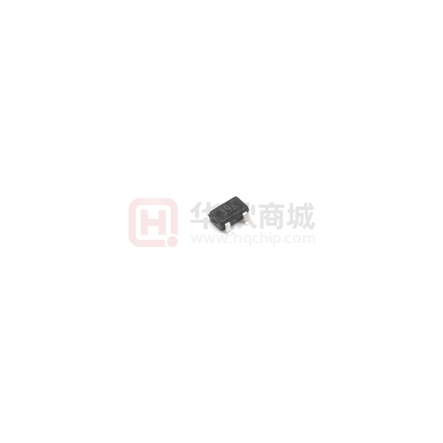
SOT-323
ID
RDS(on)MAX
���
�� ������
���
�� ����
�����
95�
�(TYP)� 1�8���
1. GATE
2. SOURCE
GENERRAL DESCRIPTION
This Single P-Channel MOSFET has been designed using advanced
Power Trench process to optimize the RDS(ON).
FEATURE
z High-Side Switching
z Low On-Resistance
z Low Threshold
z Fast Switching Speed
MARKING
3. DRAIN
APPLICATION
z Drivers:Relays, Solenoids, Lamps, Hammers, Displays, Memories
z Battery Operated Systems
z Power Supply Converter Circuits
z Load/Power Switching Cell Phones, Pagers
Equivalent Circuit
D
G
S
Maximum ratings (Ta=25℃ unless otherwise noted)
Parameter
Symbol
Value
Unit
Drain-Source voltage
VDSS
-20
Typical Gate-Source Voltage
VGS
±12
Drain Current-Continuous
ID
-0.66
Drain Current -Pulsed(note1)
IDM
-2.64
Power Dissipation (note 2)
PD
200
mW
RθJA
625
℃/W
Storage Temperature
Tj
150
Junction Temperature
Tstg
-55 ~+150
V
A
Thermal Resistance from Junction to Ambient
www.jscj-elec.com
1
℃
Rev. - 1.0
�MOSFET ELECTRICAL CHARACTERISTICS
Ta =25 ℃ unless otherwise specified
Parameter
Symbol
Test Condition
Min
Typ
Max
Unit
On/Off States
Drain-Source Breakdown Voltage
V(BR)DSS
VGS = 0V, ID =-250µA
-20
VGS(th)
VDS =VGS, ID =-250µA
-0.35
Gate-Body Leakage Current
IGSS
VDS =0V, VGS =±10V
±20
µA
Zero Gate Voltage Drain Current
IDSS
VDS =-20V, VGS =0V
-1
µA
Gate-Threshold Voltage(note 3)
Drain-Source On-State Resistance(note 3)
RDS(on)
Forward Transconductance
gFS
-0.45
- 1.1
VGS =-4.5V, ID =-1A
430
520
VGS =-2.5V, ID =-800mA
624
700
VGS =-1.8V, ID =-500mA
950
VDS =-10V, ID =-540mA
0.8
V
mΩ
S
Dynamic Characteristics(note 4)
Input Capacitance
Ciss
Output Capacitance
Coss
Reverse Transfer Capacitance
Crss
170
VDS =-16V,VGS =0V,f =1MHz
25
pF
15
Switching Times (note 4)
Turn-On Delay Time
td(on)
Rise Time
Turn-Off Delay Time
tr
td(off)
Fall Time
tf
VDD=-10V,
ID=-200mA,
VGS=-4.5V,RG=10Ω
9
5.8
ns
32.7
20.3
Drain-Source Diode Characteristics
Drain-Source Diode Forward Voltage (note 3)
VSD
IS=-0.5A, VGS = 0V
-1.2
V
Notes:
1. Repetitive Rating: Pulse width limited by maximum junction temperature.
2. This test is performed with no heat sink at Ta=25℃.
3. Pulse Test : Pulse Width≤300µs, Duty Cycle≤0.5%.
4. These parameters have no way to verify.
www.jscj-elec.com
2
Rev. - 1.0
�Typical Characteristics
Output Characteristics
Transfer Characteristics
-3.0
-2.5
VGS=-4V,-5V
VDS=-3V
Ta=25℃
(A)
-2.0
VGS=-2.5V
DRAIN CURRENT
DRAIN CURRENT
Ta=25℃
ID
-2.0
ID
(A)
VGS=-3V
Pulsed
-2.5
Pulsed
VGS=-2V
-1.5
-1.0
Ta=100℃
-1.5
-1.0
VGS=-1.5V
-0.5
-0.5
-0.0
-0.0
-0
-1
-2
-3
-4
DRAIN TO SOURCE VOLTAGE
VDS
-5
-0
(V)
-1
-2
-3
GATE TO SOURCE VOLTAGE
VGS
RDS(ON) —— VGS
RDS(ON) —— ID
1200
1000
Ta=25℃
1100
-4
(V)
Pulsed
Pulsed
900
800
(m)
VGS=-1.8V
900
800
RDS(ON)
1000
700
ON-RESISTANCE
ON-RESISTANCE
RDS(ON)
(m)
ID=-1A
700
VGS=-2.5V
600
500
Ta=100℃
600
500
Ta=25℃
400
400
VGS=-4.5V
300
-0.5
300
-0.6
-0.7
-0.8
-0.9
DRAIN CURRENT
-1.0
ID
-1.1
-1.2
-1
(A)
-2
-3
-4
GATE TO SOURCE VOLTAGE
VGS
-5
(V)
Threshold Voltage
IS —— VSD
-2
-0.8
Pulsed
-0.6
VTH
Ta=100℃
Ta=25℃
-0.1
-0.01
-0.0
-0.2
-0.4
-0.6
-0.8
SOURCE TO DRAIN VOLTAGE
www.jscj-elec.com
THRESHOLD VOLTAGE
SOURCE CURRENT
IS (A)
(V)
-1
-1.0
-1.2
ID=-250uA
-0.4
-0.2
-0.0
25
-1.4
VSD (V)
50
75
JUNCTION TEMPERATURE
3
100
TJ
125
(℃ )
Rev. - 1.0
�627�����3DFNDJH�2XWOLQH�'LPHQVLRQV�
Dimensions In Millimeters
Min
Max
0.900
1.100
0.000
0.100
0.900
1.000
0.200
0.400
0.080
0.150
2.000
2.200
1.150
1.350
2.150
2.450
0.650 TYP
1.200
1.400
0.525 REF
0.260
0.460
0°
8°
Symbol
A
A1
A2
b
c
D
E
E1
e
e1
L
L1
�
Dimensions In Inches
Min
Max
0.035
0.043
0.000
0.004
0.035
0.039
0.008
0.016
0.003
0.006
0.079
0.087
0.045
0.053
0.085
0.096
0.026 TYP
0.047
0.055
0.021 REF
0.010
0.018
0°
8°
627���� 6XJJHVWHG�3DG�/D\RXW
�
NOTICE
JSCJ reserves the right to make modifications,enhancements,improvements,corrections or other
changes without further notice to any product herein. JSCJ does not assume any liability arising
out of the application or use of any product described herein.
www.jscj-elec.com
4
Rev. - 1.0
�627�����7DSH�DQG�5HHO
SOT-323 Reel
D
I
G
W2
H
3000
2500
2000
1500
1000
D2
D1
500
W1
www.jscj-elec.com
5
Rev. - 1.0
�
很抱歉,暂时无法提供与“CJ3139KW”相匹配的价格&库存,您可以联系我们找货
免费人工找货- 国内价格
- 10+0.19929
- 100+0.19630
- 600+0.13781
- 1200+0.13643
- 3000+0.13370