JIANGSU CHANGJING ELECTRONICS TECHNOLOGY CO., LTD
SOT-23-6L Plastic-Encapsulate MOSFETS
CJL8810
Dual N-Channel MOSFET
V(BR)DSS
ID
RDS(on)TYP
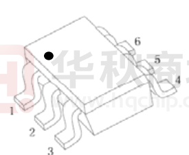
SOT-23-6L
14.5 mΩ @4.5V
20V
15.6 mΩ@3.8V
7A
18.5 mΩ @2.5V
28 mΩ@1.8V
DESCRIPTION
The CJL8810 uses advanced trench technology to provide excellent
RDS(ON) and low gate charge. It is ESD protected. This device is suitable
for use as a uni-directional or bi-directional load switch,facilitated by its
common-drain configuration.
Equivalent Circuit
MARKING:
L8810
XX
L8810=Device code
Solid point=Pin1 positioning point
XX=Date Code
MAXIMUM RATINGS (Ta=25℃ unless otherwise noted)
Parameter
Symbol
Value
Unit
Drain-Source Voltage
VDS
20
V
Gate-Source Voltage
VGS
±12
V
ID
7
A
Pulsed Drain Current
IDM *
30
A
Power Dissipation
PD
③
714
mW
③
175
℃/W
Continuous Drain Current
Thermal Resistance from Junction to Ambient
RθJA
Operation Junction and Storage Temperature Range
TJ,Tstg
-55~+150
℃
TL
260
℃
Lead Temperature for Soldering Purposes(1/8’’ from case for 10 s)
*Repetitive rating:Pluse width limited by junction temperature.
www.jscj-elec.com
1
Rev. - 2.2
�MOSFET ELECTRICAL CHARACTERISTICS
Ta =25 Я unless otherwise specified
Parameter
Symbol
Test Condition
Min
Typ
Max
Unit
STATIC PARAMETERS
Drain-source breakdown voltage
V (BR) DSS
VGS = 0V, ID = 250µA
Zero gate voltage drain current
IDSS
VDS =16V,VGS = 0V
1
µA
Gate-body leakage current
IGSS
VGS =±4.5V, VDS = 0V
±1
µA
VGS =±10V, VDS = 0V
±5
µA
1
V
Gate threshold voltage
①
VGS(th)
Drain-source on-resistance
Forward tranconductance
Diode forward voltage
①
RDS(on)
①
①
DYNAMIC PARAMETERS
VDS =VGS, ID =250µA
20
V
0.4
VGS =10V, I D = 3A
10.5
13.5
20
mΩ
VGS =4.5V, I D = 3A
11.5
14.5
22
mΩ
VGS =3.8V, I D = 3A
12.6
15.6
24
mΩ
VGS =2.5V, I D = 3A
14.5
18.5
26
mΩ
VGS =1.8V, ID = 3A
20.5
28
35
mΩ
gFS
VDS =5V, ID =7A
VSD
IS=1A, VGS = 0V
9
S
1
V
②
1150
pF
185
pF
Crss
145
pF
Total gate charge
Qg
15
nC
Gate-source charge
Qgs
0.8
nC
Qgd
3.2
nC
td(on)
6
ns
VGS=5V,VDD=10V,
13
ns
RL=1.35Ω,RGEN=3Ω
52
ns
16
ns
Input Capacitance
Ciss
Output Capacitance
Coss
Reverse Transfer Capacitance
Gate-drain charge
SWITCHING PARAMETERS
Turn-on delay time
Turn-on rise time
Turn-off delay time
Turn-off fall time
VDS =10V,VGS =0V,f =1MHz
VDS =10V,VGS =4.5V,ID =7A
②
tr
td(off)
tf
Notes :
1.
Pulse Test : Pulse width≤300µs, duty cycle≤0.5%.
2.
Guaranteed by design, not subject to production testing.
3.
The value of PD&RθJA is measured with the device one sided actived, mounted on 1 in2 FR-4 board with 2oz. Copper,
single sided, in a still air environment with Ta=25℃.
www.jscj-elec.com
2
Rev. - 2.2
�Typical Characteristics
Output Characteristics
22
VDS=5V
1.8V
12
8
15
ID
(A)
16
DRAIN CURRENT
DRAIN CURRENT
Pulsed
2.0V
ID
(A)
20
Transfer Characteristics
20
2.2V
Pulsed
1.5V
10
Ta=100℃
5
Ta=25℃
4
VGS=1.2V
0
0
1
2
3
4
DRAIN TO SOURCE VOLTAGE
RDS(ON) ——
80
5
VDS
0
6
0
1
(V)
2
3
GATE TO SOURCE VOLTAGE
ID
RDS(ON)
80
——
VGS
(V)
VGS
Ta=25℃
Ta=25℃
Pulsed
(mΩ)
ON-RESISTANCE
ON-RESISTANCE
60
RDS(ON)
60
RDS(ON)
(mΩ)
Pulsed
40
VGS=2V
20
40
ID=3A
20
VGS=10V
0
0
4
8
12
DRAIN CURRENT
ID
16
0
20
2
4
6
GATE TO SOURCE VOLTAGE
Threshold Voltage
0.80
0
(A)
10
8
VGS
10
(V)
IS —— VSD
Ta=25℃
IS (A)
0.75
0.70
SOURCE CURRENT
THRESHOLD VOLTAGE
VTH
(V)
Pulsed
ID=250uA
0.65
1
0.1
0.60
0.55
25
50
75
AMBIENT TEMPERATURE
www.jscj-elec.com
100
Ta
0.01
0.4
125
(℃ )
0.6
0.8
SOURCE TO DRAIN VOLTAGE
3
1.0
1.2
VSD (V)
Rev. - 2.2
�Typical Characteristics
NORMALIZED TRAISIENT THERMAL IMPENDANCE
10
2
NORMALIZED THERMAL IMPEDENCE, Zthja
Mounted on 1 in FR-4 board with 2oz. Copper,single sided.
In descending order
D=0.5, 0.2, 0.1, 0.05, 0.02, 0.01, Single Pulse
1
0.1
0.01
D=TON/T
RθJA=175℃/W
TJ,PK=TA+PDM×Zthja×RθJA
1E-3
1E-4
1E-6
1E-5
1E-4
1E-3
0.01
0.1
1
10
100
1000
SQUARE WAVE PULSE DURATION, tp (sec)
MAXIMUM FORWARD BIASED SAFE OPERATING AREA
100
2
Mounted on 1 in FR-4 board with 2oz. Copper,single sided.
IDM
10
d
ite
m
Li
10us
DRAIN CURRENT
ID
(A)
n
So
RD
100us
1
1ms
10ms
0.1
100ms
1s
RθJA=175℃/W
DC
TA=25℃
Single pulse
0.01
0.01
0.1
1
DRAIN TO SOURCE VOLTAGE
www.jscj-elec.com
10
VDS
BVdss
100
(V)
4
Rev. - 2.2
�SOT-23-6L Package Outline Dimensions
Symbol
A
A1
A2
b
c
D
E1
E
e
e1
L
θ
Dimensions In Millimeters
Min.
Max.
1.050
1.250
0.000
0.100
1.050
1.150
0.300
0.500
0.100
0.200
2.820
3.020
1.500
1.700
2.650
2.950
0.950(BSC)
1.800
2.000
0.300
0.600
0°
8°
Dimensions In Inches
Min.
Max.
0.041
0.049
0.000
0.004
0.041
0.045
0.012
0.020
0.004
0.008
0.111
0.119
0.059
0.067
0.104
0.116
0.037(BSC)
0.071
0.079
0.012
0.024
0°
8°
SOT-23-6L Suggested Pad Layout
NOTICE
JSCJ reserves the right to make modifications,enhancements,improvements,corrections or other
changes without further notice to any product herein. JSCJ does not assume any liability arising
out of the application or use of any product described herein.
www.jscj-elec.com
5
Rev. - 2.2
�SOT-23-6L Tape and Reel
www.jscj-elec.com
6
Rev. - 2.2
�
很抱歉,暂时无法提供与“CJL8810”相匹配的价格&库存,您可以联系我们找货
免费人工找货- 国内价格
- 5+0.43276
- 50+0.42272
- 150+0.41602
- 500+0.40932
- 国内价格
- 1+0.39090
- 3000+0.34460
- 国内价格
- 10+1.69650
- 200+1.01200
- 800+0.70840
- 3000+0.50600
- 6000+0.48070
- 30000+0.44530