JIANGSU CHANGJING ELECTRONICS TECHNOLOGY CO., LTD
���� �������������� ���! "��#���
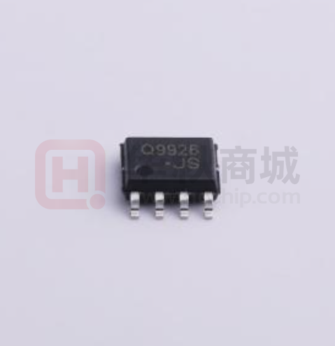
CJQ9926
Dual N-Channel MOSFET
V(BR)DSS
ID
RDS(on)MAX
40mΩ@2.5V
20V
SOP8
4.8A
30mΩ@ 4.5V
FEATURE
z
Advanced trench process technology
z
High density cell design for ultra low on-resistance
z
High power and current handing capability
z
Ideal for Liion battery pack applications
MARKING
Equivalent Circuit
Q9926= Device code
YY=Date Code
Solid dot = Pin1 indicator
Solid dot = Green molding compound device,
����if none,the normal device.
Maximum ratings (Ta=25℃ unless otherwise noted)
Symbol
Value
Unit
Drain-Source voltage
VDS
20
V
Gate-Source Voltage
VGS
±12
V
Continuous Drain Current *
ID
4.8
A
Pulsed Drain Current
IDM
30
A
Power Dissipation *
PD
1.25
W
RθJA
100
℃/ W
Junction Temperature
TJ
150
℃
Storage Temperature
Tstg
-55~+150
℃
Parameter
Thermal Resistance from Junction to Ambient *
* Surface Mounted on 1” x 1” FR4 Board.
www.jscj-elec.com
1
Rev. - 1.0
�026)(7��(/(&75,&$/�&+$5$&7(5,67,&6
Ta =25 Я unless otherwise specified
Parameter
Symbol
Test Condition
Min
Typ
Max
Unit
STATIC CHARACTERISTICS
Drain-source breakdown voltage
V (BR)DSS
VGS = 0V, ID =250µA
Zero gate voltage drain current
IDSS
VDS =20V,VGS = 0V
Gate-body leakage current
IGSS
VGS =±12V, VDS = 0V
Gate threshold voltage (note 1)
VGS(th)
VDS =VGS, ID =250µA
Drain-source on-resistance (note 1)
RDS(on)
Forward transconductance (note 1)
gFS
20
V
1
µA
±100
nA
1.0
1.2
V
VGS =2.5V, ID =5A
28
40
mΩ
VGS =4.5V, ID =6A
20
30
mΩ
VDS =15V, ID =6A
0.6
15
S
DYNAMIC CHARACTERISTICS (note 2)
Input Capacitance
Clss
Output Capacitance
Coss
Reverse Transfer Capacitance
Crss
VDS=10V,VGS=0V,
I=1.0MHz
640
pF
140
pF
80
pF
SWITCHING CHARACTERISTICS (note 2)
Turn-on delay time
td(on)
Turn-on rise time
Turn-off delay time
tr
td(off)
35
ns
VGEN=4.5V,VDD=15V,
60
ns
RGEN=6Ω, ID =1A, RL=15Ω
75
ns
Turn-off fall time
tf
30
ns
Total gate charge
Qg
20
nC
Gate-source Charge
Qgs
Gate-drain Charge
Qgd
VDS =15V,VGS =4.5V,ID =6A
3
nC
3.3
nC
SOURCE-DRAIN DIODE CHARACTERISTICS
Maximum diode forward current
Diode forward voltage (note 1)
Source-Drain Reverse Recovery Time
IS
VSD
trr
1
A
IS=1.7A,VGS=0V
1.2
V
IF = 1.7 A, di/dt = 100 A/μs
80
ns
Notes :
1. Pulse Test : Pulse Width≤300µs, Duty Cycle≤2%.
2. Guaranteed by design, not subject to production
www.jscj-elec.com
2
Rev. - 1.0
�7\SLFDO�&KDUDFWHULVWLFV
Output Characteristics
30
VGS=5.0V
4.5V
4.0V
3.5V
(A)
8
ID
20
DRAIN CURRENT
DRAIN CURRENT
2.0V
15
10
VGS=1.5V
5
0
o
Ta=25 C
2.5V
ID
(A)
25
Transfer Characteristics
10
3.0V
0
2
4
6
8
DRAIN TO SOURCE VOLTAGE
VDS
4
2
0
10
0
1
2
GATE TO SOURCE VOLTAGE
(V)
RDS(ON) —— ID
80
6
RDS(ON) ——
100
3
VGS
(V)
VGS
o
o
Ta=25 C
Ta=25 C
(mΩ)
RDS(ON)
VGS=2.5V
40
ON-RESISTANCE
ON-RESISTANCE
RDS(ON)
(mΩ)
80
60
VGS=4.5V
20
0
0
6
12
18
DRAIN CURRENT
ID
24
60
ID=6A
40
20
0
30
0
2
4
6
GATE TO SOURCE VOLTAGE
(A)
8
VGS
10
(V)
IS —— VSD
20
o
Ta=25 C
SOURCE CURRENT
IS (A)
10
3
1
0.3
0.1
0.4
0.6
0.8
1.0
SOURCE TO DRAIN VOLTAGE
www.jscj-elec.com
1.2
1.4
VSD (V)
3
Rev. - 1.0
�SOP8 Package Outline Dimensions
Symbol
A
A1
A2
b
c
D
e
E
E1
L
θ
Dimensions In Millimeters
Min
1.350
Max
1.750
Dimensions In Inches
Min
0.053
Max
0.069
0.100
0.250
1.350
1.550
0.330
0.510
0.170
0.250
4.800
5.000
1.270(BSC)
0.004
0.010
0.053
0.061
0.013
0.020
0.007
0.010
0.189
0.197
0.050(BSC)
5.800
3.800
0.400
6.200
4.000
1.270
0.228
0.150
0.016
0.244
0.157
0.050
0°
8°
0°
8°
SOP8 Suggested Pad Layout
NOTICE
JSCJ reserves the right to make modifications,enhancements,improvements,corrections or other
changes without further notice to any product herein. JSCJ does not assume any liability arising
out of the application or use of any product described herein.
www.jscj-elec.com
4
Rev. - 1.0
�SOP8 Tape and Reel
Dimensions are in millimeter
Reel Option
D
D1
D2
G
H
I
W1
W2
13''Dia
Ø330.00
100.00
13.00
R151.00
R56.00
R6.50
12.40
17.60
G.W.(kg)
REEL
4,000 pcs
www.jscj-elec.com
Reel Size
Box
13 inch
8,000 pcs
Box Size(mm)
Carton
Carton Size(mm)
360×360×65
64,000 pcs
565×380×390
5
Rev. - 1.0
�
很抱歉,暂时无法提供与“CJQ9926”相匹配的价格&库存,您可以联系我们找货
免费人工找货