JIEJIE MICROELECTRONICS CO. , Ltd
SRV05‐4 TVS Diode Array
Rev.2.0
FEATURES:
300 Watts peak pulse power per line (tP=8/20µs)
Protects four I/O lines
Low clamping voltage
Low operating voltage
Low capacitance:1.6pF typical
ROHS compliant
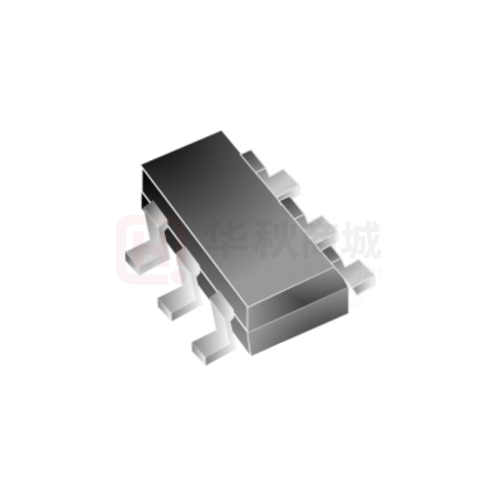
SOT23‐6L
MAIN APPLICATIONS
USB power and data line protection
Digital video interface (DVI)
Notebook computers
Video graphics cards
Monitors and flat panel displays
10/100/1000 ethernet
SIM ports
ATM interfaces
PROTECTION SOLUTION TO MEET
PIN Configuration
IEC61000-4-2 (ESD) ±30kV (air), ±30kV (contact)
IEC61000-4-4 (EFT) 40A (5/50ns)
IEC61000-4-5 (Lightning) 15A (8/20µs)
MECHANICAL CHARACTERISTICS
JEDEC SOT23-6L package
Molding compound flammability rating : UL 94V-0
Quantity per reel : 3, 000pcs
Lead finish : lead free
Marking code:5UB
TEL:+86-513-83639777
- 1 / 4-
Circuit Diagram
http://www.jjwdz.com
� SRV05‐4 TVS Diode Array
JieJie Microelectronics CO. , Ltd
ABSOLUTE MAXIMUM RATINGS (TA=25ºC, RH=45%-75%, unless otherwise noted)
Parameter
Symbol
Value
Unit
PPP
300
W
VESD
+/- 30
+/- 30
kV
Lead soldering temperature
TL
260 (10 sec.)
℃
Operating junction temperature range
TJ
-55 to +125
℃
TSTG
-55 to +150
℃
Peak pulse power dissipation on 8/20 μs
waveform
ESD per IEC 61000-4-2 (Air)
ESD per IEC 61000-4-2 (Contact)
Storage temperature range
ELECTRICAL CHARACTERISTICS (TA=25℃)
Parameter
Symbol
Reverse working voltage
Reverse breakdown voltage
Conditions
Min
Typ
VRWM
VBR
Units
5.0
IT = 1mA
6.0
V
V
Reverse leakage current
IR
VRWM = 5V
pin5 to pin2
Forward voltage
VF
IT=10mA
1.2
Clamping voltage
(I/O pin to Ground)
VC
IPP =15A, tp =8/20μs
22
CJ
VRWM = 0V, f = 1MHz
Any I/O pin to Ground
VRWM = 0V, f = 1MHz
Between I/O pins
Junction capacitance
Max
5
μA
V
24.8
V
3
pF
1.6
RATINGS AND V‐I CHARACTERISTICS CURVES (TA=25ºC, unless otherwise noted)
FIG.2: Pulse waveform (8/20μs)
FIG.1:V- I curve characteristics
(Uni-directional)
IF
Percent of IPPM
I
Peak value
100
90
front time: T1 = 1.25×T = 8×(1±20%)μs
time to half value: T2 = 20×(1±20%)μs
Half value
V C V BR V RW M
V
50
10
0
0
I PP
TEL:+86-513-83639777
T2
IR V F
IT
t(μs)
T
T1
10
20
30
40
- 2 / 4-
http://www.jjwdz.com
� SRV05‐4 TVS Diode Array
FIG.3: Pulse derating curve
JieJie Microelectronics CO. , Ltd
FIG.4: ESD clamping (8KV contact)
PPP derating in percentage(%)
100
Percent of IPPM
100
90
80
30ns
60
60ns
40
20
0
0
25
50
TA(℃)
75
100
125
150
175
10
0
0
t(ns)
tr 0.7 to 1ns
30
60
PACKAGE MECHANICAL DATA
Millimeter
Inches
Symbol
Min
Max
Min
Max
A
0.90
1.45
0.035
0.057
A1
0.00
0.15
0.000
0.006
A2
0.45
0.65
0.017
0.026
B
0.35
0.50
0.010
0.020
C
0.08
0.20
0.003
0.007
D
2.80
3.00
0.110
0.122
e
0.69
1.02
0.032
0.043
E1
1.50
1.75
0.060
0.069
E
L1
2.80BSC
0.35
0.60
0.110BSC
0.013
0.024
L
0.60
0.024
X
0.60
0.024
Y
1.10
0.043
P
3.60
0.141
P1
1.40
0.055
P2
2.50
0.098
P3
0.95
0.037
Land Pattern
TEL:+86-513-83639777
- 3 / 4-
http://www.jjwdz.com
� SRV05‐4 TVS Diode Array
JieJie Microelectronics CO. , Ltd
Information furnished in this document is believed to be accurate and reliable. However, Jiangsu
JieJie Microelectronics Co.,Ltd assumes no responsibility for the consequences of use without
consideration for such information nor use beyond it.
Information mentioned in this document is subject to change without notice, apart from that when
an agreement is signed, Jiangsu JieJie complies with the agreement.
Products and information provided in this document have no infringement of patents. Jiangsu
JieJie assumes no responsibility for any infringement of other rights of third parties which may
result from the use of such products and information.
This document is the second version which is made in 15-Apr.-2017. This document supersedes
and replaces all information previously supplied.
is a registered trademark of Jiangsu JieJie Microelectronics Co.,Ltd.
Copyright ©2017 Jiangsu JieJie Microelectronics Co.,Ltd. Printed All rights reserved.
TEL:+86-513-83639777
- 4 / 4-
http://www.jjwdz.com
�
很抱歉,暂时无法提供与“SRV05-4.TCT”相匹配的价格&库存,您可以联系我们找货
免费人工找货