CERAMIC CHIP CAPACITORS
FEATURES
• C0G (NP0), X7R, X5R, Z5U and Y5V Dielectrics
• 10, 16, 25, 50, 100 and 200 Volts
• Standard End Metalization: Tin-plate over nickel
barrier
• Available Capacitance Tolerances: ±0.10 pF; ±0.25
pF; ±0.5 pF; ±1%; ±2%; ±5%; ±10%; ±20%; and
+80%-20%
• Tape and reel packaging per EIA481-1. (See page
92 for specific tape and reel information.) Bulk
Cassette packaging (0402, 0603, 0805 only) per
IEC60286-6 and EIAJ 7201.
• RoHS Compliant
CAPACITOR OUTLINE DRAWINGS
TIN PLATE
L
W
B
T
NICKEL PLATE
S
ELECTRODES
CONDUCTIVE
METALLIZATION
DIMENSIONS—MILLIMETERS AND (INCHES)
METRIC
SIZE CODE
L - LENGTH
W - WIDTH
0201*
0603
0.6 (.024) ± .03 (.001)
0.3 ± (.012) ± .03 (.001)
0.15 (.006) ± .05 (.002)
N/A
0402*
1005
1.0 (.04) ± .05 (.002)
0.5 (.02) ± .05 (.002)
0.20 (.008) -.40 (.016)
0.3 (.012)
B - BANDWIDTH
0603
1608
1.6 (.063) ± .15 (.006)
0.8 (.032) ± .15 (.006)
0.35 (.014) ± .15 (.006)
0.7 (.028)
0805*
2012
2.0 (.079) ± .20 (.008)
1.25 (.049) ± .20 (.008)
0.50 (.02) ± .25 (.010)
0.75 (.030)
1206*
3216
3.2 (.126) ± .20 (.008)
1.6 (.063) ± .20 (.008)
0.50 (.02) ± .25 (.010)
N/A
1210*
3225
3.2 (.126) ± .20 (.008)
2.5 (.098) ± .20 (.008)
1808
4520
4.5 (.177) ± .30 (.012)
2.0 (.079) ± .20 (.008)
See page 78
for thickness
dimensions.
0.50 (.02) ± .25 (.010)
N/A
0.60 (.024) ± .35 (.014)
N/A
N/A
1812
4532
4.5 (.177) ± .30 (.012)
3.2 (.126) ± .30 (.012)
0.60 (.024) ± .35 (.014)
1825*
4564
4.5 (.177) ± .30 (.012)
6.4 (.252) ± .40 (.016)
0.60 (.024) ± .35 (.014)
N/A
2220
5650
5.6 (.220) ± .40 (.016)
5.0 (.197) ± .40 (.016)
0.60 (.024) ± .35 (.014)
N/A
2225
5664
5.6 (.220) ± .40 (.016)
6.3 (.248) ± .40 (.016)
0.60 (.024) ± .35 (.014)
N/A
MOUNTING
TECHNIQUE
Solder Reflow
Solder Wave +
or
Solder Reflow
Solder Reflow
* Note: Indicates EIA Preferred Case Sizes (Tightened tolerances apply for 0402, 0603, and 0805 packaged in bulk bassette, see page 96.)
+ For extended value 1210 case size - solder reflow only.
CAPACITOR ORDERING INFORMATION (Standard Chips - For
C 0805 C 103 K 5 R A C*
CERAMIC
SIZE CODE
SPECIFICATION
C - Standard
CAPACITANCE CODE
Expressed in Picofarads (pF)
First two digits represent significant figures.
Third digit specifies number of zeros. (Use 9
for 1.0 through 9.9pF. Use 8 for 0.5 through 0.99pF)
(Example: 2.2pF = 229 or 0.50 pF = 508)
CAPACITANCE TOLERANCE
B – ±0.10pF J – ±5%
C – ±0.25pF K – ±10%
D – ±0.5pF
M – ±20%
F – ±1%
P – (GMV) – special order only
G – ±2%
Z – +80%, -20%
72
Military see page 87)
END METALLIZATION
C-Standard (Tin-plated nickel barrier)
FAILURE RATE LEVEL
A- Not Applicable
TEMPERATURE CHARACTERISTIC
Designated by Capacitance
Change Over Temperature Range
G – C0G (NP0) (±30 PPM/°C)
R – X7R (±15%) (-55°C + 125°C)
P– X5R (±15%) (-55°C + 85°C)
U – Z5U (+22%, -56%) (+10°C + 85°C)
V – Y5V (+22%, -82%) (-30°C + 85°C)
VOLTAGE
1 -- 100V
1
100V 3 - 25V
3 - 25V
2 - 200V 4 - 16V
2
200V
4 - 16V
5 - 50V 8 - 10V
5
50V
8 - 10V
6 - 35V 9 - 6.3V
* Part Number Example: C0805C103K5RAC (14 digits - no spaces)
7 - 4V
7 - 4V
9 - 6.3V
©KEMET Electronics Corporation, P.O. Box 5928, Greenville, S.C. 29606, (864) 963-6300
Ceramic Surface Mount
T
THICKNESS
S
SEPARATION
minimum
EIA SIZE
CODE
�CERAMIC CHIP/STANDARD
C0G CAPACITANCE RANGE – 1210, 1812, 1825, 2220, 2225
CAP.
PF
10
12
15
18
22
27
33
39
47
56
68
82
100
120
150
180
220
270
330
390
470
560
680
820
1000
1200
1500
1800
2200
2700
3300
3900
4700
5600
6800
8200
10,000
12,000
15,000
18,000
22,000
27,000
33,000
CAP
CODE
100
120
150
180
220
270
330
390
470
560
680
820
101
121
151
181
221
271
331
391
471
561
681
821
102
122
152
182
222
272
332
392
472
562
682
822
103
123
153
183
223
273
333
Cap
CAP. Cap
pF
Code
TOL.
0.5-2.4 508-249
C ,D2.7-9.1 J279-919
,M
,K
10.0-13.0 100-130
C ,D
,K ,M
15.0-24.0 J150-240
27.0-51.0
C ,D
G ,J270-510
,K ,M
56.0-82.0 560-820
C91.0-360.0
,D
G ,J910-361
,K ,M
C ,D 390.0
,M
391
G ,J ,K
430.0
431
D,F
,M
,G
,J
,K
470.0
471
D,F
,M
,G ,J ,K
510.0
511
560.0
561
D,F
,M
,G ,J ,K
620.0
621
D,F
,M
,G ,J ,K
680.0
681
750.0
751
F
,M
,G ,J ,K
820.0
821
F
,M
,G ,J ,K
910.0
911
F,G ,J ,K
,M
102
1,000.0
112
1,100.0
F,G ,J ,K
,M
122
1,200.0
F,G ,J ,K
,M
132
1,300.0
152
1,500.0
F,G ,J ,K
,M
162
1,600.0
F,G ,J ,K
,M
182
1,800.0
F,G ,J ,K
,M
202
2,000.0
222
2,200.0
F,G ,J ,K
,M
242
2,400.0
F,G ,J ,K
,M
272
2,700.0
302
3,000.0
F,G ,J ,K
,M
332
3,300.0
F,G ,J ,K
,M
362
3,600.0
392
3,900.0
F,G ,J ,K
,M
432
4,300.0
F,G ,J ,K
,M
472
4,700.0
F,G ,J ,K
,M
512
5,100.0
562
5,600.0
F,G ,J ,K
,M
622
6,200.0
F
,M
,G
,J
,K
682
6,800.0
752
7,500.0
F,G ,J ,K
,M
822
8,200.0
F
,M
,G
,J
,K
912
9,100.0
F,G ,J ,K
,M
103
10,000.0
123
12,000.0
F,G ,J ,K
,M
153
15,000.0
F,G ,J ,K
,M
183
18,000.0
223
22,000.0
F,G ,J ,K
,M
273
27,000.0
F
,M
,G
,J
,K
333
33,000.0
F,G ,J ,K
,M
473
47,000.0
563
56,000.0
F
,M
,G
,J
,K
683
68,000.0
F,G ,J ,K
,M
823
82,000.0
104
100,000.0
F,G ,J ,K
,M
124
120,000.0
F,G ,J ,K
,M
154
150,000.0
224
220,000.0
F,G ,J ,K
,M
274
270,000.0
F
,M
,G
,J
,K
334
330,000.0
F,G ,J ,K
,M
474
470,000.0
564
560,000.0
F,G ,J ,K
,M
Cap
Tolerance 10V
D
. FB
D FB K,MFBFB
D
J,K,M FB
DFB
G,J,K,MFBFB
D,F,G,J,K,M
FBFB
FB
F,G,J,K,M FB
FB
F,G,J,K,MFBFB
FB
F,G,J,K,MFBFB
F,G,J,K,MFBFB
FB
F,G,J,K,M FB
FB
F,G,J,K,MFBFB
F,G,J,K,MFBFB
FB
F,G,J,K,M FB
FB
F,G,J,K,MFBFB
F,G,J,K,MFBFB
FB
F,G,J,K,M FB
FB
FB
F,G,J,K,M FB
FB
F,G,J,K,MFBFB
F,G,J,K,MFBFB
FB
F,G,J,K,M FB
FB
F,G,J,K,MFBFB
F,G,J,K,MFBFB
FB
F,G,J,K,M FB
FB
FB
F,G,J,K,M FB
FB
F,G,J,K,MFBFB
F,G,J,K,MFBFB
FB
F,G,J,K,M FB
FB
F,G,J,K,MFBFB
F,G,J,K,MFBFB
FB
F,G,J,K,M FB
FB
F,G,J,K,MFBFB
F,G,J,K,MFBFB
FB
F,G,J,K,MFBFB
FB
F,G,J,K,M FF
FB
F,G,J,K,MFBFB
F,G,J,K,MFBFB
FB
F,G,J,K,M FB
FB
F,G,J,K,MFBFB
F,G,J,K,MFBFC
FB
F,G,J,K,M FC
FB
FB
F,G,J,K,M FE
FB
F,G,J,K,MFC
FF
F,G,J,K,MFC
FG
FB
F,G,J,K,M FG
FB
F,G,J,K,MFFFB
F,G,J,K,MFFFB
FB
F,G,J,K,M FB
FF
F,G,J,K,MFFFB
FB
F,G,J,K,MFFFB
F,G,J,K,MFG
FB
FB
F,G,J,K,M FB
FC
F,G,J,K,M FC
F,G,J,K,M FE
FF
F,G,J,K,M FG
FG
F,G,J,K,M FH
F,G,J,K,M FK+
F,G,J,K,M
F,G,J,K,M
F,G,J,K,M
F,G,J,K,M
C1210*
16V 25V
FB FB
FB
FBFB
FB FB
FBFB
FB
FB
FBFB
FB FB
FBFB
FB
FBFB
FB
FB
FBFB
FB FB
FBFB
FB
FB
FBFB
FB FB
FBFB
FB
FB
FBFB
FB FB
FB
FB FB
FBFB
FB
FB
FBFB
FB FB
FBFB
FB
FB
FBFB
FB FB
FB
FB FB
FBFB
FB
FB
FBFB
FB FB
FBFB
FB
FB
FBFB
FB FB
FBFB
FB
FB
FBFB
FB
FBFB
FF FF
FBFB
FB
FB
FBFB
FB FB
FBFB
FB
FC
FEFC
FC FC
FE
FE FE
FGFF
FF
FG
FCFG
FG FG
FFFB
FB
FB FB
FB FB
FB FB
FB FB
FB FB
FB FB
FC FC
FE FE
FG FG
FH FH
FK+ FK+
C1812*
C1825*
50V 100V 200V 50V 100V 200V
FB FB
FB
FB FB
FB
FB FB
FB
FB FB
FB
FB FB
FB
FB FB
FB
FB FB
FB
FB FB
FB
FB FB
FB
FB FB
FB GB GB GB
FB FB
FB
FB FB
FB GB GB GB
FB FB
FB
FB FB
FB GB GB GB
FB FB
FB
FB FB
FB GB GB GB
FB FB
FB
FB FB
FB GB GB GB
FB FB
FB
FB FB
FB GB GB GB
FB FB
FC
FB FB
FE GB GB GB
FB FB
FE
FB FB
FE GB GB GB
FB FC
FE
FB FC
FG GB GB GB
FB FC
FC
FB FC
FC GB GB GB
FB FC
FF
FB
FF
FF GB GB GB
FB
FF
FF
FB
FF
FF GB GB GB
FB
FF
FF
FF FG
FG GB GB GD
FB FG
FG
FB FG
FG GB GB GH
FB FG
FB FG
GB GB GJ
FC FC
FC FC
GB GH
FE FE
FF
FF
GB GH
FG FB
GB GG
FG FB
GB GB
FB FB
GB GB
FB FB
GB GB
FB FB
GB GB
FB FB
GB GB
FB FE
GB GB
FB
FF
GB GB
FC FG
GB GB
FF FH
GB GB
FG FM+
GB GD
FH
GB GH
FM+
GD GN
GK
C2220
C2225
50V 100V 200V 50V 100V 200V 50V 100V 200V
HB
HB
HB
HB
HB
HB
KB
KB
KB
HB
HB
HB
KB
KB
KB
HB
HB
HB
JB
JB
KB
KB
KB
HB
HB
HB
JB
JB
KB
KB
KB
HB
HB
HB
HB
HB
HB
HB
HB
HB
HE
HE
HF
HE
HE
JB
JB
JB
JB
JB
JB
JB
JB
JB
JB
JB
JB
JB
JB
JB
JB
JD
JG
JB
JB
JB
JB
JB
JB
JB
JB
JB
JB
JB
JB
JB
JB
JD
JF
JH
KB
KB
KB
KB
KB
KB
KB
KB
KB
KB
KB
KB
KE
KB
KB
KE
F,G ,J ,K ,M
X7R CAPACITANCE RANGE – 0402, 0603, 0805, 1206
Cap
pF
Cap
Code
Cap Tol
150
180
220
270
330
390
470
560
680
820
1,000
1,200
1,500
1,800
2,200
2,700
3,300
3,900
4,700
5,600
6,800
8,200
10,000
12,000
15,000
18,000
22,000
27,000
33,000
39,000
47,000
56,000
68,000
82,000
100,000
120,000
150,000
180,000
220,000
270,000
330,000
390,000
470,000
560,000
680,000
820,000
1,000,000
1,200,000
1,500,000
1,800,000
2,200,000
2,700,000
3,300,000
3,900,000
4,700,000
5,600,000
6,800,000
8,200,000
10,000,000
151
181
221
271
331
391
471
561
681
821
102
122
152
182
222
272
332
392
472
562
682
822
103
123
153
183
223
273
333
393
473
563
683
823
104
124
154
184
224
274
334
394
474
564
684
824
105
125
155
185
225
275
335
395
475
565
685
825
106
J, K, M
J, K, M
J, K, M
J, K, M
J, K, M
J, K, M
J, K, M
J, K, M
J, K, M
J, K, M
J, K, M
J, K, M
J, K, M
J, K, M
J, K, M
J, K, M
J, K, M
J, K, M
J, K, M
J, K, M
J, K, M
J, K, M
J, K, M
J, K, M
J, K, M
J, K, M
J, K, M
J, K, M
J, K, M
J, K, M
J, K, M
J, K, M
J, K, M
J, K, M
J, K, M
J, K, M
J, K, M
J, K, M
J, K, M
J, K, M
J, K, M
J, K, M
J, K, M
J, K, M
J, K, M
J, K, M
J, K, M
J, K, M
J, K, M
J, K, M
J, K, M
J, K, M
J, K, M
J, K, M
J, K, M
J, K, M
J, K, M
J, K, M
J, K, M
C0603
C0402
6.3V
BB
BB
BB
BB
BB
BB
BB
BB
BB
BB
BB
BB
BB
BB
BB
BB
BB
BB
BB
BB
BB
BB
BB
BB
BB
BB
BB
BB
BB
BB
BB
BB
BB
BB
BB
10V
BB
BB
BB
BB
BB
BB
BB
BB
BB
BB
BB
BB
BB
BB
BB
BB
BB
BB
BB
BB
BB
BB
BB
BB
BB
BB
BB
BB
BB
BB
BB
BB
BB
BB
BB
16V
BB
BB
BB
BB
BB
BB
BB
BB
BB
BB
BB
BB
BB
BB
BB
BB
BB
BB
BB
BB
BB
BB
BB
BB
BB
BB
BB
BB
BB
BB
BB
BB
BB
BB
BB
25V
BB
BB
BB
BB
BB
BB
BB
BB
BB
BB
BB
BB
BB
BB
BB
BB
BB
BB
BB
BB
BB
BB
BB
BB
BB
BB
BB
BB
BB
BB
BB
50V
BB
BB
BB
BB
BB
BB
BB
BB
BB
BB
BB
BB
BB
BB
BB
BB
BB
BB
BB
BB
BB
BB
BB
BB
BB
BB
BB
C0805
6.3V
10V
16V
25V
50V
CB
CB
CB
CB
CB
CB
CB
CB
CB
CB
CB
CB
CB
CB
CB
CB
CB
CB
CB
CB
CB
CB
CB
CB
CB
CB
CB
CB
CB
CB
CB
CB
CB
CB
CB
CB
CB
CB
CB
CB
CB
CB
CB
CB
CB
CB
CB
CB
CB
CB
CB
CB
CB
CB
CB
CB
CB
CB
CB
CB
CB
CB
CB
CB
CB
CB
CB
CB
CB
CB
CB
CB
CB
CB
CB
CB
CB
CB
CB
CB
CB
CB
CB
CB
CB
CB
CB
CB
CB
CB
CB
CB
CB
CB
CB
CB
CB
CB
CB
CB
CB
CB
CB
CB
CB
CB
CB
CB
CB
CB
CB
CB
CB
CB
CB
CB
CB
CB
CB
CB
CB
CB
CB
CB
CB
CB
CB
CB
CB
CB
CB
CB
CB
CB
CB
CB
CB
CB
CB
CB
CB
CB
CB
CB
CB
CB
CB
CB
CB
CB
CB
CB
CB
CB
CB
CB
CB
CB
CB
CB
CB
CB
CB
CB
CB
CB
CB
CB
CB
CB
CB
CB
CB
CB
CB
CB
CB
CB
CB
CB
CB
CB
CB
CB
CB
CB
CB
CB
CB
CB
CB
CB
CB
CB
CB
CD
CC*
CC*
CC*
CD
100V 200V 6.3V
CB
CB
CB
CB
CB
CB
CB
CB
CB
CB
CB
CB
CB
CB
CB
CB
CB
CB
CB
CB
CB
CB
CB
CB
CB
CB
CB
CB
CB
CB
CB
CB
CB
CB
CB
CB
CB
CB
CB
CB
CB
CB
CB
CB
CB
CB
CB
CB
CB
CB
CB
CB
DC
DC
DC
DC
DC
DC
DC
DC
DC
DC
DC
DC
DC
DC
DC
DC
DC
DC
DC
DC
DC
DC
DC
DC
DC
DC
DC
DC
DC
DC
DD
DD
DD
DD
DC
DC
DC
DC
DD
DD
DG
DD
DD
DD
DD
DD
DE
DG
DG
DG
C1206
10V
16V
25V
50V
DC
DC
DC
DC
DC
DC
DC
DC
DC
DC
DC
DC
DC
DC
DC
DC
DC
DC
DC
DC
DC
DC
DC
DC
DC
DC
DC
DC
DC
DC
DD
DD
DD
DD
DC
DC
DC
DC
DD
DD
DG
DD
DD
DD
DD
DD
DE
DG
DG
DG
DC
DC
DC
DC
DC
DC
DC
DC
DC
DC
DC
DC
DC
DC
DC
DC
DC
DC
DC
DC
DC
DC
DC
DC
DC
DC
DC
DC
DC
DC
DD
DD
DD
DD
DC
DC
DC
DC
DD
DD
DG
DD
DD
DD
DD
DD
DE
DG
DG
DG
DC
DC
DC
DC
DC
DC
DC
DC
DC
DC
DC
DC
DC
DC
DC
DC
DC
DC
DC
DC
DC
DC
DC
DC
DC
DC
DC
DC
DC
DC
DD
DD
DD
DD
DC
DC
DC
DC
DD
DD
DG
DD
DG
DG
DG
DG
DC
DC
DC
DC
DC
DC
DC
DC
DC
DC
DC
DC
DC
DC
DC
DC
DC
DC
DC
DC
DC
DC
DC
DC
DC
DC
DC
DC
DC
DC
DD
DD
DD
DD
DD
DD
DD
DD
100V 200V 6.3V
DC
DC
DC
DC
DC
DC
DC
DC
DC
DC
DC
DC
DC
DC
DC
DC
DC
DC
DC
DC
DC
DC
DC
DD
DD
DD
DD
DD
DD
DE
DE
DE
DE
DE
DG
DG
DD
DE
DE
DH
DH
DC
DC
DC
DC
DC
DC
DC
DC
DC
DC
DC
DC
DC
DC
DC
DC
DC
DC
DC
DC
DC
DC
DC
DC
DC
DC
DE
DE
DE
DG
DG
EB
EB
EB
EB
EB
EB
EB
EB
EB
EB
EB
EB
EB
EB
EB
EB
EB
EB
EB
EB
EB
EB
EB
EB
EB
EC
EC
EC
EC
EB
EB
EB
EC
ED
EE
EF
EF
ED
EF
EF
ED
EN
ED
EF
EF+
EH+
EH+
EH+
EH+
10V
16V
25V
50V
EB
EB
EB
EB
EB
EB
EB
EB
EB
EB
EB
EB
EB
EB
EB
EB
EB
EB
EB
EB
EB
EB
EB
EB
EB
EC
EC
EC
EC
EB
EB
EB
EC
ED
EE
EF
EF
ED
EF
EF
ED
EN
ED
EF
EF+
EH+
EH+
EH+
EH+
EB
EB
EB
EB
EB
EB
EB
EB
EB
EB
EB
EB
EB
EB
EB
EB
EB
EB
EB
EB
EB
EB
EB
EB
EB
EC
EC
EC
EC
EB
EB
EB
EC
ED
EE
EF
EF
ED
EF
EF
ED
EN
ED
EF
EF+
EH+
EH+
EH+
EH+
EB
EB
EB
EB
EB
EB
EB
EB
EB
EB
EB
EB
EB
EB
EB
EB
EB
EB
EB
EB
EB
EB
EB
EB
EB
EC
EC
EC
EC
EB
EB
EB
EC
ED
EE
EF
EG
EG
EG
EB
EB
EB
EB
EB
EB
EB
EB
EB
EB
EB
EB
EB
EB
EB
EB
EB
EB
EB
EB
EB
EB
EB
EB
EB
EC
EC
EC
EC
EC
EC
EC
EC
EC
ED
ED
ED
EH
EH
EH
EH
* Capacitance K or M. ontact KEMET Sales Rep for J tolerance availability. +_ Reflow Only.
NOTE: For non-standard capacitance values or voltages, contact your local KEMET sales representative.
# X7R dielectric - Extended Range Values - Cap and DF measured @ 0.5 Vrms.
Improved product with higher ratings and tighter capacitance tolerance product may be substituted within the same size (length, width, and thickness) at KEMET's option.
Reels with such substitutions will be marked with the improved KEMET part numbers.
page
78Thickness
for Thickness
Reference
Chart.
SeeSee
page
63 for
CodeCode
Reference
Chart.
74
©KEMET Electronics Corporation, P.O. Box 5928, Greenville, S.C. 29606, (864) 963-6300
EF
EH
EH+
100V 200V
EB
EB
EB
EB
EB
EB
EB
EB
EB
EB
EB
EB
EB
EB
EB
EB
EB
EB
EB
EC
EC
EB
EB
EB
EB
EC
EC
EC
EC
EM
EG
EG
EG
EB
EB
EB
EB
EB
EB
EB
EB
EB
EB
EB
EB
EB
EB
EB
EB
EB
EB
EB
EB
ED
ED
ED
ED
EM
EM
EG
�CERAMIC CHIP/STANDARD
X7R CAPACITANCE RANGE – 1210, 1808, 1812, 1825, 2220, 2225
Cap
pF
2,200
2,700
3,300
3,900
4,700
5,600
6,800
8,200
10,000
12,000
15,000
18,000
22,000
27,000
33,000
39,000
47,000
56,000
68,000
82,000
100,000
120,000
150,000
180,000
220,000
270,000
330,000
390,000
470,000
560,000
680,000
820,000
1,000,000
1,200,000
1,500,000
1,800,000
2,200,000
2,700,000
3,300,000
3,900,000
4,700,000
5,600,000
6,800,000
8,200,000
10,000,000
12,000,000
15,000,000
18,000,000
22,000,000
47,000,000
Cap
Cap Tol.
Code
6.3V
222
272
332
392
472
562
682
822
103
123
153
183
223
273
333
393
473
563
683
823
104
124
154
184
224
274
334
394
474
564
684
824
105
125
155
185
225
275
335
395
475
565
685
825
106
126
156
186
226
476
J,K,M
J,K,M
J,K,M
J,K,M
J,K,M
J,K,M
J,K,M
J,K,M
J,K,M
J,K,M
J,K,M
J,K,M
J,K,M
J,K,M
J,K,M
J,K,M
J,K,M
J,K,M
J,K,M
J,K,M
J,K,M
J,K,M
J,K,M
J,K,M
J,K,M
J,K,M
J,K,M
J,K,M
J,K,M
J,K,M
J,K,M
J,K,M
J,K,M
J,K,M
J,K,M
J,K,M
J,K,M
J,K,M
J,K,M
J,K,M
J,K,M
J,K,M
J,K,M
J,K,M
J,K,M
J,K,M
J,K,M
J,K,M
J,K,M
M
FB
FB
FB
FB
FB
FB
FB
FB
FB
FB
FB
FB
FB
FB
FB
FB
FB
FB
FB
FB
FB
FB
FC
FC
FC
FC
FD
FD
FD
FD
FD
FF
FH
FH
FH
FH
FJ
FE
FF
FG
FC+
FF+
FG+
FH+
FH+
C1210
C1808
10V
16V
25V
50V
FB
FB
FB
FB
FB
FB
FB
FB
FB
FB
FB
FB
FB
FB
FB
FB
FB
FB
FB
FB
FB
FB
FC
FC
FC
FC
FD
FD
FD
FD
FD
FF
FH
FH
FH
FH
FJ
FE
FF
FG
FC+
FF+
FG+
FH+
FH+
FB
FB
FB
FB
FB
FB
FB
FB
FB
FB
FB
FB
FB
FB
FB
FB
FB
FB
FB
FB
FB
FB
FC
FC
FC
FC
FD
FD
FD
FD
FD
FF
FH
FH
FH
FH
FJ
FE
FF
FG
FC+
FF+
FG+
FH+
FH+
FB
FB
FB
FB
FB
FB
FB
FB
FB
FB
FB
FB
FB
FB
FB
FB
FB
FB
FB
FB
FB
FB
FC
FC
FC
FC
FD
FD
FD
FD
FD
FF
FH
FH
FH
FH
FJ
FB
FB
FB
FB
FB
FB
FB
FB
FB
FB
FB
FB
FB
FB
FB
FB
FB
FB
FB
FB
FB
FB
FC
FC
FC
FC
FD
FD
FD
FD
FD
FF
FH
FG
FG
FG
FG
FM
FM
FG+
FS+
100V 200V
FB
FB
FB
FB
FB
FB
FB
FB
FB
FB
FB
FB
FB
FB
FB
FB
FB
FB
FB
FC
FD
FD
FD
FD
FD
FD
FD
FB
FB
FB
FB
FB
FB
FB
FB
FB
FB
FB
FB
FB
FB
FB
FB
FC
FC
FC
FF
FG
50V
LD
LD
LD
LD
LD
LD
LD
LD
LD
LD
LD
LD
LD
LD
LD
LD
LD
LD
LD
LD
C1812
100V 200V
LD
LD
LD
LD
LD
LD
LD
LD
LD
LD
LD
LD
LD
LD
LD
LD
LD
LD
LD
LD
LD
LD
FD
FM
25V
50V
GB
GB
GB
GB
GB
GB
GB
GB
GB
GB
GB
GB
GB
GB
GB
GB
GB
GB
GB
GB
GB
GB
GB
GC
GC
GE
GE
GB
GB
GB
GB
GB
GB
GB
GB
GB
GB
GB
GB
GB
GB
GB
GB
GB
GB
GB
GB
GB
GB
GB
GC
GC
GE
GE
FT*
C1825
100V 200V
GB
GB
GB
GB
GB
GB
GB
GB
GB
GB
GB
GB
GB
GB
GB
GB
GB
GB
GB
GG
GG
GG
GG
GG
GG
GG
GG
50V
GB
GB
GB
GB
GB
GB
GB
GB
GB
GB
GB
GB
GB
GB
GB
GB
GE
GF
GG
GG
GG
GG
GJ
HB
HB
HB
HB
HB
HB
HB
HB
HB
HB
HB
HB
HB
HB
HB
HB
HB
HB
HB
HB
HB
HB
HC
HD
HF
GO°
GK*
C2220
100V 200V
HB
HB
HB
HB
HB
HB
HB
HB
HB
HB
HB
HB
HB
HB
HB
HB
HB
HD
HD
25V
HB
HB
HB
HB
HB
HB
HB
HB
HB
HB
HB
HB
HB
HB
HB
HD
HD
HD
HD
HF
HF
50V
JC
JC
JC
JC
JC
JC
JC
JC
JC
JC
JD
JF
JC
JC
JC
JC
JC
JC
JC
JC
JC
JC
JD
JF
JF
JO
C2225
100V 200V
JC
JC
JC
JC
JC
JD
JF
JF
JC
JC
JC
JC
JC
JC
JC
JC
JC
JC
JD
JD
JF
JF
50V
KC
KC
KC
KC
KC
KC
KC
KC
KC
KB
KB
KB
KB
KB
KB
KB
KB
KB
KC
KD
KD
100V 200V
KC
KC
KC
KC
KC
KC
KC
KC
KC
KC
KC
KC
KC
KC
KC
KC
KD
KC
KC
KC
KC
KC
KC
KC
KC
KC
KC
KC
KC
KD
KD
KD
KE
KE
KE
GK*
FM+
FS+
GK*
JO
FS+
FS+
FS+
JO
* Capacitance tolerance K or M. Contact your local KEMET Sales Rep for J tolerance availablity. + Reflow Only
NOTE: For non-standard capacitance values or voltages, contact your local KEMET sales representative.
50 Volt Ceramic Chips can be used for 63 volt applications.
# Extended Range Values – Cap and DF measured @ 0.5 Vrms.
° M tolerance only
Ceramic Surface Mount
Improved product with higher ratings and tighter capacitance tolerance product may be substituted within the same size (length, width, and thickness) at KEMET's option.
Reels with such substitutions will be marked with the improved KEMET part numbers.
Y5V CAPACITANCE RANGE
Cap
pF
Cap
Code
22,000
27,000
33,000
39,000
47,000
56,000
68,000
82,000
100,000
120,000
150,000
180,000
220,000
270,000
330,000
390,000
470,000
560,000
680,000
820,000
1,000,000
1,200,000
1,500,000
1,800,000
2,200,000
3,300,000
4,700,000
5,600,000
6,800,000
10,000,000
15,000,000
22,000,000
223
273
333
393
473
563
683
823
104
124
154
184
224
274
334
394
474
564
684
824
105
125
155
185
225
335
475
565
685
106
156
226
C0402*
C0603*
Cap
Tol. 6.3V 10V 16V 6.3V 10V 16V
Z
BB BB BB CB CB CB
Z
BB BB BB CB CB CB
Z
BB BB BB CB CB CB
Z
BB BB BB CB CB CB
Z
BB BB BB CB CB CB
Z
BB BB BB CB CB CB
Z
BB BB BB CB CB CB
Z
BB BB BB CB CB CB
Z
BB BB BB CB CB CB
Z
CC CC CC
Z
CC CC CC
Z
CC CC CC
Z
BB
CC CC CC
Z
CC CC CC
Z
CC CC CC
Z
CC CC CC
Z
BB
CC CC CC
Z
CC CC
Z
CC CC
Z
CC CC
Z
BB
CC CC
Z
Z
Z
Z
Z
Z
Z
Z
Z
C0805*
25V 6.3V 10V
CB
CB
CB
CB
CB
CB
CB
CB
CB
CC DC DC
CC DC DC
CC DC DC
CC DC DC
CC DC DC
CC DC DC
DC DC
DC DC
DD DD
DE DE
DG DG
DG DG
DC DC
DC DC
DD DD
DD DD
DE DE
DH DH
DH DH
DH DH
DH DH
16V 25V 50V
DC
DC
DC
DD
DD
DD
DD
DD
DD
DC DC
DC DC
DC DC
DC DC DD
DC DC
DC DC
DC DC
DC DC
DD DD
DE DE
DG DG
DG DG
DC
DC
DD
DD
DH
DH
C1206*
C1210*
6.3V 10V 16V 25V 50V 6.3V 10V 16V 25V 50V
EB
EB
EB
EB
EB
EB
EB
EB
EB
EC
EB
EB
EB
EC
EB
EB
EB
EG
EC
EC
EC
EE
EF
EM
EJ
EJ
EJ
Z
Z
EH
EC
EB
EB
EB
EC
EB
EB
EB
EG
EC
EC
EC
EE
EF
EM
EJ
EJ
EJ
EC
EB
EB
EB
EC
EB
EB
EB
EG
EC
EC
EC
EE
EF
EM
EJ
EC
EB
EB
EB
EC
EB
EB
EB
EG
FD
FD
FD
FD
FD
FD
FD
FF
FH
FD
FD
FD
FD
FE
FG
FG
FH
FH
FH
FT
FD
FD
FD
FD
FD
FD
FD
FF
FH
FD
FD
FD
FD
FE
FG
FG
FH
FH
FH
FT
FD
FD
FD
FD
FD
FD
FD
FF
FH
FD
FD
FD
FD
FE
FG
FG
FH
FH
FH
FM
FD
FD
FD
FD
FD
FD
FD
FF
FH
FD
FD
FD
FD
FD
FD
FD
FF
FH
NOTE: For non-standard capacitance values or voltages, contact your local KEMET sales representative.
50 Volt Ceramic Chips can be used for 63 volt applications.
* EIA preferred chip sizes
+ Reflow only
See page 78 for Thickness Code Reference Chart
©KEMET Electronics Corporation, P.O. Box 5928, Greenville, S.C. 29606, (864) 963-630
75
�CERAMIC CHIP CAPACITORS
Thickness Code Reference Chart
Packaging Quantity Based on Finished Chip Thickness Specifications
Thickness
Code
Chip
Size
Chip Thickness
Range (mm)
Qty per Reel
7" Plastic
Qty per Reel
13" Plastic
Qty per Reel
7" Paper
Qty per Reel
13" Paper
Qty per Bulk
Cassette
AA
BB
CB
CC
CD
DB
DC
DD
DE
DF
DG
DH
DJ
DK
DL
EB
EC
ED
EE
EF
EG
EH
EJ
EK
EL
EM
EN
FB
FC
FD
FE
FF
FG
FH
FJ
FK
FL
FM
FN
FO
FP
FQ
FR
FS
FT
LD
GB
GC
GD
GE
GF
GG
GH
GJ
GK
GL
GM
GN
GO
HB
HC
HD
HE
HF
JB
JC
JD
JE
JF
JG
JH
JO
KB
KC
KD
KE
0201
0402
0603
0603
0603
0805
0805
0805
0805
0805
0805
0805
0805
0805
0805
1206
1206
1206
1206
1206
1206
1206
1206
1206
1206
1206
1206
1210
1210
1210
1210
1210
1210
1210
1210
1210
1210
1210
1210
1210
1210
1210
1210
1210
1210
1808
1812
1812
1812
1812
1812
1812
1812
1812
1812
1812
1812
1812
1812
1825
1825
1825
1825
1825
2220
2220
2220
2220
2220
2220
2220
2220
2225
2225
2225
2225
0.30 ± 0.03
0.50 ± 0.05
0.80 ± 0.07
0.80 ± 0.10
0.80 ± 0.15
0.60 ± 0.10
0.78 ± 0.10
0.90 ± 0.10
1.00 ± 0.10
1.10 ± 0.10
1.25 ± 0.15
1.25 ± 0.20
1.25 ± 0.20
1.25 ± 0.15
0.95 ± 0.10
0.78 ± 0.10
0.90 ± 0.10
1.00 ± 0.10
1.10 ± 0.10
1.20 ± 0.15
1.60 ± 0.15
1.60 ± 0.20
1.70 ± 0.20
0.80 ± 0.10
1.15 ± 0.15
1.25 ± 0.15
0.95 ± 0.10
0.78 ± 0.10
0.90 ± 0.10
0.95 ± 0.10
1.00 ± 0.10
1.10 ± 0.10
1.25 ± 0.15
1.55 ± 0.15
1.85 ± 0.20
2.10 ± 0.20
1.40 ± 0.15
1.70 ± 0.20
1.85 ± 0.20
1.50 ± 0.20
1.60 ± 0.20
2.50 ± 0.22
2.25 ± 0.20
2.50 ± 0.20
1.90 ± 0.20
0.90 ± 0.10
1.00 ± 0.10
1.10 ± 0.10
1.25 ± 0.15
1.30 ± 0.10
1.50 ± 0.10
1.55 ± 0.10
1.40 ± 0.15
1.70 ± 0.15
1.60 ± 0.20
1.90 ± 0.20
2.00 ± 0.20
1.70 ± 0.20
2.50 ± 0.20
1.10 ± 0.15
1.15 ± 0.15
1.30 ± 0.15
1.40 ± 0.15
1.50 ± 0.15
1.00 ± 0.15
1.10 ± 0.15
1.30 ± 0.15
1.40 ± 0.15
1.50 ± 0.15
1.70 ± 0.15
1.80 ± 0.15
2.40 ± 0.15
1.00 ± 0.15
1.10 ± 0.15
1.30 ± 0.15
1.40 ± 0.15
N/A
N/A
N/A
N/A
N/A
N/A
N/A
N/A
2,500
2,500
2,500
2,500
3,000
3,000
4,000
4,000
4,000
2,500
2,500
2,500
2,000
2,000
2,000
2,000
2,000
2,500
4,000
4,000
4,000
4,000
2,500
2,500
2,500
2,000
2,000
2,000
2,000
2,000
2,000
2,000
2,000
1,500
2,000
1,000
1,500
4,000
1,000
1,000
1,000
1,000
1,000
1,000
1,000
1,000
1,000
1,000
1,000
1,000
500
1,000
1,000
1,000
1,000
1,000
1,000
1,000
1,000
1,000
1,000
1,000
1,000
500
1,000
1,000
1,000
1,000
N/A
N/A
N/A
N/A
N/A
N/A
N/A
N/A
10,000
10,000
10,000
10,000
N/A
N/A
10,000
10,000
10,000
10,000
10,000
10,000
8,000
8,000
8,000
8,000
8,000
10,000
10,000
10,000
10,000
10,000
10,000
10,000
10,000
8,000
8,000
8,000
8,000
8,000
8,000
8,000
8,000
N/A
8,000
4,000
4,000
10,000
4,000
4,000
4,000
4,000
4,000
4,000
4,000
4,000
4,000
4,000
4,000
4,000
N/A
4,000
4,000
4,000
4,000
4,000
4,000
4,000
4,000
4,000
4,000
4,000
4,000
2,000
4,000
4,000
4,000
4,000
15,000
10,000
4,000
4,000
4,000
4,000
4,000
4,000
N/A
N/A
N/A
N/A
N/A
N/A
N/A
4,000
N/A
N/A
N/A
N/A
N/A
N/A
N/A
N/A
N/A
N/A
N/A
N/A
N/A
N/A
N/A
N/A
N/A
N/A
N/A
N/A
N/A
N/A
N/A
N/A
N/A
N/A
N/A
N/A
N/A
N/A
N/A
N/A
N/A
N/A
N/A
N/A
N/A
N/A
N/A
N/A
N/A
N/A
N/A
N/A
N/A
N/A
N/A
N/A
N/A
N/A
N/A
N/A
N/A
N/A
N/A
N/A
N/A
N/A
N/A
N/A
N/A
50,000
10,000
10,000
10,000
10,000
10,000
10,000
N/A
N/A
N/A
N/A
N/A
N/A
N/A
10,000
N/A
N/A
N/A
N/A
N/A
N/A
N/A
N/A
N/A
N/A
N/A
N/A
N/A
N/A
N/A
N/A
N/A
N/A
N/A
N/A
N/A
N/A
N/A
N/A
N/A
N/A
N/A
N/A
N/A
N/A
N/A
N/A
N/A
N/A
N/A
N/A
N/A
N/A
N/A
N/A
N/A
N/A
N/A
N/A
N/A
N/A
N/A
N/A
N/A
N/A
N/A
N/A
N/A
N/A
N/A
N/A
N/A
N/A
N/A
N/A
N/A
50,000
15,000
N/A
N/A
10,000
N/A
N/A
N/A
N/A
N/A
N/A
N/A
N/A
N/A
N/A
N/A
N/A
N/A
N/A
N/A
N/A
N/A
N/A
N/A
N/A
N/A
N/A
N/A
N/A
N/A
N/A
N/A
N/A
N/A
N/A
N/A
N/A
N/A
N/A
N/A
N/A
N/A
N/A
N/A
N/A
N/A
N/A
N/A
N/A
N/A
N/A
N/A
N/A
N/A
N/A
N/A
N/A
N/A
N/A
N/A
N/A
N/A
N/A
N/A
N/A
N/A
N/A
N/A
N/A
N/A
N/A
N/A
N/A
N/A
N/A
This chart refers to ceramic chip thickness codes on pages 73 – 76.
Note: TU suffix represents tape and reel packaging of unmarked components.
Note: TM suffix represents tape and reel packaging of marked components.
Cases sizes d1210 are 8mm tape with 4mm pitch and Case Sizes >1210 are 12mm tape and 8mm pitch.
Thisart
ch refers
to ceramic chip thickness codes on pages 73-76.
78
©KEMET Electronics Corporation, P.O. Box 5928, Greenville, S.C. 29606, (864) 963-6300
�CERAMIC CHIP CAPACITORS
Packaging Information
Tape & Reel Packaging
KEMET offers Multilayer Ceramic Chip Capacitors
packaged in 8mm and 12mm plastic tape on 7" and
13" reels in accordance with EIA standard 481-1:
Taping of surface mount components for automatic
handling. This packaging system is compatible with all
tape fed automatic pick and place systems. See page 78
for details on reeling quantities for commercial chips
and page 87 for MIL-PRF-55681 chips.
g
handling. This packaging system is compatible with all
tape fed automatic pick and place systems. See page 81
for details on reeling quantities for commercial chips
and page 90 for MIL-PRF-55681 chips.
Anti-Static Reel
Embossed Carrier*
0402 and 0603 case sizes
available on punched paper only.
®
T
ME
KE
Chip Orientation
in Pocket
(except 1825 Commercial, and 1825 & 2225 Military)
Embossment
8mm ±.30
(.315 ±.012")
or
12mm ±.30
(.472 ±.012")
178mm (7.00")
or
330mm (13.00")
Anti-Static Cover Tape
(.10mm (.004") Max Thickness)
* Punched paper carrier used for 0402 and 0603 case size.
Case Sizes ≤ 1210 are 8 mm tape with 4 mm pitch.
Case Sizes >1210 are 12 mm tape with 8 mm pitch.
Note: TU suffix represents tape and reel packaging of unmarked components.
TM suffix represents tape and reel packaging of marked components.
SURFACE MOUNT LAND DIMENSIONS - CERAMIC CHIP CAPACITORS - MM
Reflow Solder
Dimension
0402
0603
0805
1206
1210
1812
1825
2220
2225
CourtyardC
C
X
X
GG
Y
Z
Z
Y
Z
2.14
2.78
3.30
4.50
4.50
5.90
5.90
7.00
7.00
G
0.28
0.68
0.70
1.50
1.50
2.30
2.30
3.30
3.30
X Y(ref) C(ref)
0.74 0.93 1.21
1.08 1.05 1.73
1.60 1.30 2.00
2.00 1.50 3.00
2.90 1.50 3.00
3.70 1.80 4.10
6.90 1.80 4.10
5.50 1.85 5.15
6.80 1.85 5.15
Wave Solder
Z
G
X
Y(ref) Smin
Not Recommended
3.18
3.70
4.90
4.90
0.68
0.70
1.50
1.50
0.80
1.10
1.40
2.00
1.25
1.50
1.70
1.70
1.93
2.20
3.20
3.20
Not Recommended
Packaging
Grid
Grid
placement
courtyard
Placement
Calculation Formula
Z = Lmin + 2Jt + Tt
G = Smax - 2Jh -Th
X = Wmin + 2Js + Ts
Tt, Th, Ts = Combined tolerances
©KEMET Electronics Corporation, P.O. Box 5928, Greenville, S.C. 29606, (864) 963-6300
93
�TANTALUM, CERAMIC AND
ALUMINUM CHIP CAPACITORS
Packaging Information
Performance Notes
1. Cover Tape Break Force: 1.0 Kg Minimum.
2. Cover Tape Peel Strength: The total peel strength of the cover tape from the carrier tape shall be:
Tape Width
Peel Strength
8 mm
0.1 Newton to 1.0 Newton (10g to 100g)
12 mm
0.1 Newton to 1.3 Newton (10g to 130g)
The direction of the pull shall be opposite the direction of the carrier tape travel. The pull angle of the carrier
tape shall be 165� to 180� from the plane of the carrier tape. During peeling, the carrier and/or cover tape
shall be pulled at a velocity of 300 ±10 mm/minute.
3. Reel Sizes: Molded tantalum capacitors are available on either 180 mm (7") reels (standard) or 330 mm (13")
reels (with C-7280). Note that 13” reels are preferred.
4. Labeling: Bar code labeling (standard or custom) shall be on the side of the reel opposite the sprocket holes.
Refer to EIA-556.
Embossed Carrier Tape Configuration: Figure 1
Table 1 — EMBOSSED TAPE DIMENSIONS (Metric will govern)
Constant Dimensions — Millimeters (Inches)
Tape Size
8 mm
and
12 mm
D0
E
1.5
1.75 ±0.10
+0.10 -0.0
(0.059
(0.069 ±0.004)
+0.004, -0.0)
P0
P2
T Max
T1 Max
4.0 ±0.10
2.0 ±0.05
0.600
0.100
(0.157 ±0.004)
(0.079 ±0.002)
(0.024)
(0.004)
Variable Dimensions — Millimeters (Inches)
Tape Size
Pitch
B1 Max.
Note 1
D1 Min.
Note 2
F
P1
R Min.
Note 3
T2 Max
W
8 mm
Single
(4 mm)
4.4
1.0
3.5 ±0.05
4.0 ±0.10
25.0
2.5
8.0 ±0.30
(.315 ±0.012)
12 mm
Double
(8 mm)
(0.173)
(0.039) (0.138 ±0.002)
(0.157 ±0.004) (0.984)
(0.098)
8.2
(0.323)
1.5
5.5 ±0.05
(0.059) (0.217 ±0.002)
8.0 ±0.10
30.0
(0.315 ±0.004) (1.181)
4.6
12.0 ±0.30
(0.181) (0.472 ±0.012)
A0B0K0
Note 4
NOTES
1. B1 dimension is a reference dimension for tape feeder clearance only.
2. The embossment hole location shall be measured from the sprocket hole controlling the location of the embossment. Dimensions of
embossment location and hole location shall be applied independent of each other.
3. Tape with components shall pass around radius “R” without damage (see sketch A). The minimum trailer length (Fig. 2) may require
additional length to provide R min. for 12 mm embossed tape for reels with hub diameters approaching N min. (Table 2)
4. The cavity defined by A0, B0, and K0 shall be configured to surround the part with sufficient clearance such that the chip does not protrude beyond the sealing plane of the cover tape, the chip can be removed from the cavity in a vertical direction without mechanical
restriction, rotation of the chip is limited to 20 degrees maximum in all 3 planes, and lateral movement of the chip is restricted to 0.5 mm
maximum in the pocket (not applicable to vertical clearance.)
94
©KEMET Electronics Corporation, P.O. Box 5928, Greenville, S.C. 29606, (864) 963-6300
�TANTALUM, CERAMIC AND
ALUMINUM CHIP CAPACITORS
Packaging Information
Embossed Carrier Tape Configuration (cont.)
20°
Sketch D: Tape Camber (Top View)
1mm (0.039) Max.
1mm (0.039) Max.
250mm (9.843)
Allowable camber to be 1 mm/250 mm.
400mm (15.75) Min.
Figure 2:
Tape Leader
& Trailer
Dimensions
(Metric
Dimensions
Will Govern)
Packaging
Figure 3: Reel Dimensions (Metric Dimensions will govern)
Table 2 – REEL DIMENSIONS (Metric will govern)
Tape Size
8 mm
A Max
330.0
(12.992)
B* Min
1.5
(0.059)
C
13.0 ± 0.20
(0.512 ± 0.008)
D* Min
20.2
(0.795)
12 mm
330.0
(12.992)
1.5
(0.059)
13.0 ± 0.20
(0.512 ± 0.008)
20.2
(0.795)
N Min
50.0
(1.969)
See
Note 3
Table 1
W1
8.4
+1.5, -0.0
(0.331
+0.059, -0.0)
12.4
+2.0, -0.0
(0.488
+0.078, -0.0)
W2 Max
14.4
(0.567)
18.4
(0.724)
©KEMET Electronics Corporation, P.O. Box 5928, Greenville, S.C. 29606, (864) 963-6300
W3
7.9 Min
(0.311)
10.9 Max
(0.429)
11.9 Min
(0.469)
15.4 Max
(0.606)
95
�CERAMIC CHIP CAPACITORS
Packaging Information
Punched Carrier (Paper Tape) Configuration (Ceramic Chips Only):
10 pitches cumulative
tolerance on tape
±0.2 (±0.008)
P0
T
P2
D0
E
Top
Tape
Cover
Bottom
Tape
Cover
A0
F
W
B0
G2
T1
P1
User Direction of Feed
Center lines
of cavity
Max. Cavity Size
See Note 1
Table 1
Table 1: 8 & 12mm Punched Tape
(Metric Dimensions Will Govern)
Constant Dimensions - Millimeters (Inches)
Tape
Size
D0
P0
E
T1
P2
G1
G2
R Min.
8mm
1.5
1.75 ±0.10
4.0 ± 0.10
2.0 ± 0.05
0.10 0.75 0.75 25 (.984)
and
+0.10, -0.0
(.004) (.030) (.030) See Note 2
12mm
(.059
(.069 ±0.004) (.157 ± 0.004) (.079 ± 0.002) Max. Min. Min.
Table 1
+0.004, -0.0)
Table 1: 8 & 12mm Punched Tape
(Metric Dimensions Will Govern)
Variable Dimensions - Millimeters (Inches)
Tape
Size
8mm
1/2
Pitch
P1
2.0 ± 0.10
(.079 ±.004)
3.5 ± 0.05
See Requirements
Section 3.3 (d) (.138 ± .002)
8mm
4.0 ± 0.10
(0.157 ± .004)
12mm
4.0 ± 0.10
(0.157 ± .004)
A0B0
W
F
5.5 ± 0.05
12mm
8.0 ± 0.10
(.217 ± .002)
Double (0.315 ± .004)
Pitch
8.0 ± 0.3
(.315 ± 0.012)
See Note 1
Table 1
12.0 ± 0.3
T
1.1mm (.043)
Max. for Paper
Base Tape and
1.6mm (.063)
Max. for NonPaper Base
Compositions.
See Note 3.
(.472 ± .012)
Note:
1. A0, B0 and T determined by the maximum dimensions to the ends of the terminals extending from the
body and/or the body dimensions of the component. The clearance between the ends of the terminals or
body of the component to the sides and depth of the cavity (A0, B0 and T) must be within 0.05mm (.002)
minimum and 0.50mm (.020) maximum. The clearance allowed must also prevent rotation of the component
within the cavity of not more than 20 degrees (see sketches A and B).
2. Tape with components shall pass around radius "R" without damage.
3. KEMET nominal thicknesses are: 0402 = 0.6mm and all others 0.95mm minimum.
Sketch A:
Bending Radius
See Note 2
Table 1
Sketch B:
Max. Component
Rotation - Front
Cross Sectional View
R
(Min.)
20°
96
Sketch C:
Component Rotation - Top View
Maximum
20° component rotation.
Typical
component
center line
©KEMET Electronics Corporation, P.O. Box 5928, Greenville, S.C. 29606, (864) 963-6300
�CERAMIC CHIP CAPACITORS
Packaging Information
Bulk Cassette Packaging (Ceramic Chips only)
Table 2 – Capacitance Values Available
In Bulk Cassette Packaging
6.8 ± 0.1
8.8 ± 0.1
12.0 ± 0.1
(Meets Dimensional Requirements IEC-286-6 and EIAJ 7201)
53.3*
2.0 ±
31.5 ± 0.2
0
3.0 ±
0.1
0
0
0.1
0.2
0
0402
All
All
All
All
0603
All
All
All
All
0805
C0G
200
100
50
109
109
109
181
331
102
X7R
200
100
50
25
16
221
221
221
221
221
392
103
273
104
104
Y5V
25
16
104
104
224
224
19.0*
1.5 ±
Unit: mm
* Reference
36 ± 00.2
10*
Min. Max.
Case
Cap Cap
Size Dielectric Voltage Value Value
5.0*
110 ± 0.7
Table 1 – Capacitor Dimensions for Bulk
Cassette Packaging – Millimeters
Metric
Size
Code
EIA
Size
Code
1005
1608
2012
0402
0603
0805
Length
L
Width
W
Thickness Bandwidth
T
B
1.0 ± 0.05 0.5 ± 0.05
1.6 ± 0.07 0.8 ± 0.07
2.0 ± 0.10 1.25 ± 0.10
0.5 ± .05
0.8 ± .07
0.6 ± .10
0.2 to 0.4
0.2 to 0.5
0.5 to 0.75
Minimum
Separation
S
Number of
Pcs/Cassette
0.3
0.7
0.75
50,000
15,000
10,000
Terminations: KEMET nickel barrier layer with a tin overplate.
CAPACITOR MARKING TABLE
(Marking Optional - Not Available
for 0402 Size or Y5V Dielectric)
9
0
1
2
3
4
5
6
7
A
B
C
D
E
F
G
H
J
K
L
M
N
P
Q
R
S
T
U
V
W
X
Y
Z
a
b
d
e
f
m
n
t
y
0.10
0.11
0.12
0.13
0.15
0.16
0.18
0.20
0.22
0.24
0.27
0.30
0.33
0.36
0.39
0.43
0.47
0.51
0.56
0.62
0.68
0.75
0.82
0.91
0.25
0.35
0.40
0.45
0.50
0.60
0.70
0.80
0.90
1.0
1.1
1.2
1.3
1.5
1.6
1.8
2.0
2.2
2.4
2.7
3.0
3.3
3.6
3.9
4.3
4.7
5.1
5.6
6.2
6.8
7.5
8.2
9.1
2.5
3.5
4.0
4.5
5.0
6.0
7.0
8.0
9.0
10
11
12
13
15
16
18
20
22
24
27
30
33
36
39
43
47
51
56
62
68
75
82
91
25
35
40
45
50
60
70
80
90
100
110
120
130
150
160
180
200
220
240
270
300
330
360
390
430
470
510
560
620
680
750
820
910
250
350
400
450
500
600
700
800
900
1000
1100
1200
1300
1500
1600
1800
2000
2200
2400
2700
3000
3300
3600
3900
4300
4700
5100
5600
6200
6800
7500
8200
9100
2500
3500
4000
4500
5000
6000
7000
8000
9000
10,000
11,000
12,000
13,000
15,000
16,000
18,000
20,000
22,000
24,000
27,000
30,000
33,000
36,000
39,000
43,000
47,000
51,000
56,000
62,000
68,000
75,000
82,000
91,000
25,000
35,000
40,000
45,000
50,000
60,000
70,000
80,000
90,000
100,000
110,000
120,000
130,000
150,000
160,000
180,000
200,000
220,000
240,000
270,000
300,000
330,000
360,000
390,000
430,000
470,000
510,000
560,000
620,000
680,000
750,000
820,000
910,000
250,000
350,000
400,000
450,000
500,000
600,000
700,000
800,000
900,000
1,000,000
1,100,000
1,200,000
1,300,000
1,500,000
1,600,000
1,800,000
2,000,000
2,200,000
2,400,000
2,700,000
3,000,000
3,300,000
3,600,000
3,900,000
4,300,000
4,700,000
5,100,000
5,600,000
6,200,000
6,800,000
7,500,000
8,200,000
9,100,000
2,500,000
3,500,000
4,000,000
4,500,000
5,000,000
6,000,000
7,000,000
8,000,000
9,000,000
10,000,000
11,000,000
12,000,000
13,000,000
15,000,000
16,000,000
18,000,000
20,000,000
22,000,000
24,000,000
27,000,000
30,000,000
33,000,000
36,000,000
39,000,000
43,000,000
47,000,000
51,000,000
56,000,000
62,000,000
68,000,000
75,000,000
82,000,000
91,000,000
25,000,000
35,000,000
40,000,000
45,000,000
50,000,000
60,000,000
70,000,000
80,000,000
90,000,000
Laser marking is available as an extra-cost option for
most KEMET ceramic chips. Such marking is two
sided, and includes a K to identify KEMET, followed by
two characters (per EIA-198 - see table below) to
identify the capacitance value. Note that marking is
not available for size 0402 nor for any Y5V chip. In
addition, the 0603 marking option is limited to the K
only.
KA3
Example shown is 1,000 pF capacitor.
©KEMET Electronics Corporation, P.O. Box 5928, Greenville, S.C. 29606, (864) 963-6300
Packaging
Capacitance (pF) For Various Numeral Identifiers
Numeral
Alpha
Character
97
�KEMET Electronics - KEMET Ceramic P/N Suffixes - Marking & Packaging
Page 1 of 2
CONTACT US | CUSTOMER SERVICE
Search here for KEMET PN, Competitor PN, Partial PN, or Part Description
Search here for General Keywords, Part Series, or Corporate Information
KE Home
Search
FAQs
Technical Articles
Created: 04/17/2000
Updated: 08/28/2009
Contact Us
Help
Product: Ceramic
Categories: Labeling, Packaging, Part Markings, Part Number
KEMET Ceramic P/N Suffixes - Marking & Packaging
Description :
KEMET Ceramic P/N Suffixes - Marking & Packaging
Answer :
KEMET ceramic chips are available marked or unmarked (preferred) in several packaging styles. These ordering
details are included as suffixes to the KEMET 14 digit part number, and will be used during the order entry
process by KEMET sales personnel and distributors. (Notice that ordering a KEMET part number without a suffix
will result in shipment of unmarked chips loose packed in a bag - so be sure to use a suffix if other packaging is
needed.)
To speed up the ordering process, we use "shortcut" suffixes for the most common ordering modes. The most
popular shortcut ordering suffix is "TU", which indicates unmarked chips, in labelled 7" tape & reel packaging.
Alternatively, ordering suffix "TM" indicates marked chips, in labelled 7" reels. However, remember that marked
chips are less likely to be in stock, and will have a cost premium associated with marking. Details on marking
appear in our catalog, available on the website. Note that all 0402 chips and all Y5V chips are not available
marked.
Other special ordering suffixes also exist, covering options such as 13" reels, bulk cassette, and bulk in bag
packaging. In addition, special customer requirements will also be included in custom ordering suffixes, up to 2
groups of 4 numerical digits each.
When the capacitors are shipped, the labels will be printed with the 14 digit KEMET part number, plus the
numerical suffixes ordered (or corresponding to the shortcut suffixes). These will include one or more 4 digit
numerical suffix(es), which indicate the exact mode of marking and packaging. These will be based on the
information given to KEMET sales at the time of order entry, and and are detailed in the following table. (Note - to
improve delivery, marked chips may occasionally be supplied when unmarked are acceptable.)
CATEGORY
DESCRIPTION
Unmarked
Marking Required
(Marking not available for
any 0402 or Y5V chips)
Standard Reeling
7" Plastic Tape
0805 - 2225 (0402, 0603 &
0805 thickness DB, DC & DD
are reeled only on paper)
7800 (same as "TU")
7025 (same as "TM")
Standard Reeling
7" Paper Tape
0402 & 0603
7867(same as "TU")
7013(same as "TM")
Special Reeling
13" Plastic Tape
0805 - 2225 (0402, 0603 &
0805 thickness DB, DC & DD
are reeled only on paper)
7210
7215
Special Reeling
7" Paper Tape
0805 (0.78 mm thickness selected values only)
7867 & 9239
7013 & 9239
Special Reeling
7" Paper Tape
1206 - 1210 (selected values
only)
7867
7013
Special Reeling
13" Paper Tape
0402 & 0603
7411
7040
Special Reeling
13" Paper Tape
0805 (0.78 mm thickness selected values only)
7411 & 9239
7040 & 9239
Special Reeling
13" Paper Tape
1206 - 1210 (selected values
only)
7411
7040
Special Packaging
Bulk Cassette for
0402, 0603 & 0805.
0402's are never
marked.
Use ONLY with special 0.6
mm 0805.
9028
9028 & 3325
Special Packaging
Loose Chips in Plastic
Bags
0603 - 2225
No Suffix
3325
Technical Papers featured
at CARTS Europe 2007:
Aluminium Electrolytic Capacitors' performance in Very High Ripple
Current and Temperature Applications
Reliability and Critical Applications of Tantalum Capacitors
Click here for a full listing
of our Technical Papers
BME C0G MLCCs: The High Capacitance Class-I Solution
Soldering of SMD Film Capacitors in Practical Lead Free
Processes
D-Pack 3D Interposer Decoupling System
Study of MnO2 Coverage on Ta Capacitors with High CV Powders
ESR Stabilization of Ta Capacitors for Automotive Applications in
Severe Environmental Conditions
The Battle for Maximum Volumetric Efficiency - Part 1: When
Technologies Compete, Customers Win
Improved Ripple Current Capability with Facedown Terminations
The Battle for Maximum Volumetric Efficiency - Part 2:
Advancements in Solid Electrolyte Capacitors
http://www.kemet.com/kemet/web/homepage/kfbk3.nsf/vaFeedbackFAQ/3B46726C01571... 8/28/2009
�CERAMIC CHIP/CAPACITORS
Tin Lead L Termination
FEATURES
KEMET’s line of Tin/Lead termination commercial MLCC surface mount capacitors are designed to meet the needs of the
commercial, high reliability, and military customer applications where Tin/Lead plating is required. KEMET’s Tin/Lead electroplating process is designed to meet a 5% minimum lead content in the termination of the component. As the bulk of the
electronics industry marches to RoHS compliance it is important that KEMET provide the Tin/Lead terminated products for
our valued high reliability and military customers.
KEMET Tin/Lead MLCC surface mount capacitors are available in standard EIA case sizes from 0402 to 2225 and standard
KEMET
Tiin/Lead
MLCC
surface
mount
capacitors
are available
in standard
EIA to
case
sizes
0402
to 2225 and
standard
capacitance
values
in X7R
and C0G
dielectrics.
Voltage
ratings range
from 6.3V
200V.
Tofrom
order
the Tin/Lead
terminations
th
capacitance
values
X7R,
X5R,
C0G
dielectrics.
Voltage
ratings
range
from
6.3V to 200V.
To order
themount
Tin/Lead
terminaindicate an “L”
in thein14
digit
of
the
part
number.
To
request
the
L
Series
termination
for
other
surface
product
lines (Open
th
tions
an “L” in
the 14etc.)
digit
part number.
For additional
and voltage
contact
the facMode,indicate
High Voltage,
Arrays,
or of
forthe
additional
dielectrics
and higherdielectrics
voltage ratings,
pleaseratings
contactplease
the factory
or local
Sales
tory or local Sales personnel.
representative.
CAPACITOR OUTLINE DRAWINGS
W
T
L
Sn/Pb PLATE
B
NICKEL PLATE
S
ELECTRODES
CONDUCTIVE METALLIZATION
DIMENSIONS—MILLIMETERS AND (INCHES)
METRIC
SIZE CODE
L - LENGTH
W - WIDTH
0201*
0603
0.6 (.024) ± .03 (.001)
0.3 ± (.012) ± .03 (.001)
0.15 (.006) ± .05 (.002)
N/A
0402*
1005
1.0 (.04) ± .05 (.002)
0.5 (.02) ± .05 (.002)
0.20 (.008) -.40 (.016)
0.3 (.012)
B - BANDWIDTH
0603
1608
1.6 (.063) ± .15 (.006)
0.8 (.032) ± .15 (.006)
0.35 (.014) ± .15 (.006)
0.7 (.028)
0805*
2012
2.0 (.079) ± .20 (.008)
1.25 (.049) ± .20 (.008)
0.50 (.02) ± .25 (.010)
0.75 (.030)
1206*
3216
3.2 (.126) ± .20 (.008)
1.6 (.063) ± .20 (.008)
0.50 (.02) ± .25 (.010)
N/A
1210*
3225
3.2 (.126) ± .20 (.008)
2.5 (.098) ± .20 (.008)
1808
4520
4.5 (.177) ± .30 (.012)
2.0 (.079) ± .20 (.008)
See page 78
for thickness
dimensions.
0.50 (.02) ± .25 (.010)
N/A
0.60 (.024) ± .35 (.014)
N/A
N/A
1812
4532
4.5 (.177) ± .30 (.012)
3.2 (.126) ± .30 (.012)
0.60 (.024) ± .35 (.014)
1825*
4564
4.5 (.177) ± .30 (.012)
6.4 (.252) ± .40 (.016)
0.60 (.024) ± .35 (.014)
N/A
2220
5650
5.6 (.220) ± .40 (.016)
5.0 (.197) ± .40 (.016)
0.60 (.024) ± .35 (.014)
N/A
2225
5664
5.6 (.220) ± .40 (.016)
6.3 (.248) ± .40 (.016)
0.60 (.024) ± .35 (.014)
N/A
MOUNTING
TECHNIQUE
Solder Reflow
Solder Wave +
or
Solder Reflow
Solder Reflow
* Note: Indicates EIA Preferred Case Sizes (Tightened tolerances apply for 0402, 0603, and 0805 packaged in bulk cassette, see page 96.)
† For extended value 1210 case size – solder reflow only.
CAPACITOR ORDERING INFORMATION (Standard Chips - For
Military see page 87)
C 0805 C 103 K 5 R A L*
CERAMIC
SIZE CODE
SPECIFICATION
C - Standard
CAPACITANCE CODE
Expressed in Picofarads (pF)
First two digits represent significant figures.
Third digit specifies number of zeros. (Use 9
for 1.0 through 9.9pF. Use 8 for 0.5 through 0.99pF)
(Example: 2.2pF = 229 or 0.50 pF = 508)
CAPACITANCE TOLERANCE
B – ±0.10pF J – ±5%
C – ±0.25pF K – ±10%
D – ±0.5pF
M – ±20%
F – ±1%
G – ±2%
* Part Number Example: C0805C103K5RAL
END METALLIZATION
L - SnPb plated nickel barrier
(SnPb 5% minimum)
FAILURE RATE LEVEL
A- Not Applicable
TEMPERATURE CHARACTERISTIC
Designated by Capacitance
Change Over Temperature Range
G – C0G (NP0) (±30 PPM/°C)
R – X7R (±15%) (-55°C + 125°C)
P – X5R (±15%) (-55°C + 85°C)
VOLTAGE
1 - 100V
3 - 25V
2 - 200V
4 - 16V
5 - 50V
8 - 10V
9 - 6.3V
6 - 35V
(14 digits - no spaces)
Refer to pages 73-76 for NP0/C0G, X7R and X5R dielectric capacitance ranges available.
©KEMET Electronics Corporation, P.O. Box 5928, Greenville, S.C. 29606, (864) 963-6300
77
Ceramic Surface Mount
T
THICKNESS
S
SEPARATION
minimum
EIA SIZE
CODE
�CERAMIC CHIP CAPACITORS
Thickness Code Reference Chart
Packaging Quantity Based on Finished Chip Thickness Specifications
Thickness
Code
Chip
Size
Chip Thickness
Range (mm)
Qty per Reel
7" Plastic
Qty per Reel
13" Plastic
Qty per Reel
7" Paper
Qty per Reel
13" Paper
Qty per Bulk
Cassette
AA
BB
CB
CC
CD
DB
DC
DD
DE
DF
DG
DH
DJ
DK
DL
EB
EC
ED
EE
EF
EG
EH
EJ
EK
EL
EM
EN
FB
FC
FD
FE
FF
FG
FH
FJ
FK
FL
FM
FN
FO
FP
FQ
FR
FS
FT
LD
GB
GC
GD
GE
GF
GG
GH
GJ
GK
GL
GM
GN
GO
HB
HC
HD
HE
HF
JB
JC
JD
JE
JF
JG
JH
JO
KB
KC
KD
KE
0201
0402
0603
0603
0603
0805
0805
0805
0805
0805
0805
0805
0805
0805
0805
1206
1206
1206
1206
1206
1206
1206
1206
1206
1206
1206
1206
1210
1210
1210
1210
1210
1210
1210
1210
1210
1210
1210
1210
1210
1210
1210
1210
1210
1210
1808
1812
1812
1812
1812
1812
1812
1812
1812
1812
1812
1812
1812
1812
1825
1825
1825
1825
1825
2220
2220
2220
2220
2220
2220
2220
2220
2225
2225
2225
2225
0.30 ± 0.03
0.50 ± 0.05
0.80 ± 0.07
0.80 ± 0.10
0.80 ± 0.15
0.60 ± 0.10
0.78 ± 0.10
0.90 ± 0.10
1.00 ± 0.10
1.10 ± 0.10
1.25 ± 0.15
1.25 ± 0.20
1.25 ± 0.20
1.25 ± 0.15
0.95 ± 0.10
0.78 ± 0.10
0.90 ± 0.10
1.00 ± 0.10
1.10 ± 0.10
1.20 ± 0.15
1.60 ± 0.15
1.60 ± 0.20
1.70 ± 0.20
0.80 ± 0.10
1.15 ± 0.15
1.25 ± 0.15
0.95 ± 0.10
0.78 ± 0.10
0.90 ± 0.10
0.95 ± 0.10
1.00 ± 0.10
1.10 ± 0.10
1.25 ± 0.15
1.55 ± 0.15
1.85 ± 0.20
2.10 ± 0.20
1.40 ± 0.15
1.70 ± 0.20
1.85 ± 0.20
1.50 ± 0.20
1.60 ± 0.20
2.50 ± 0.22
2.25 ± 0.20
2.50 ± 0.20
1.90 ± 0.20
0.90 ± 0.10
1.00 ± 0.10
1.10 ± 0.10
1.25 ± 0.15
1.30 ± 0.10
1.50 ± 0.10
1.55 ± 0.10
1.40 ± 0.15
1.70 ± 0.15
1.60 ± 0.20
1.90 ± 0.20
2.00 ± 0.20
1.70 ± 0.20
2.50 ± 0.20
1.10 ± 0.15
1.15 ± 0.15
1.30 ± 0.15
1.40 ± 0.15
1.50 ± 0.15
1.00 ± 0.15
1.10 ± 0.15
1.30 ± 0.15
1.40 ± 0.15
1.50 ± 0.15
1.70 ± 0.15
1.80 ± 0.15
2.40 ± 0.15
1.00 ± 0.15
1.10 ± 0.15
1.30 ± 0.15
1.40 ± 0.15
N/A
N/A
N/A
N/A
N/A
N/A
N/A
N/A
2,500
2,500
2,500
2,500
3,000
3,000
4,000
4,000
4,000
2,500
2,500
2,500
2,000
2,000
2,000
2,000
2,000
2,500
4,000
4,000
4,000
4,000
2,500
2,500
2,500
2,000
2,000
2,000
2,000
2,000
2,000
2,000
2,000
1,500
2,000
1,000
1,500
4,000
1,000
1,000
1,000
1,000
1,000
1,000
1,000
1,000
1,000
1,000
1,000
1,000
500
1,000
1,000
1,000
1,000
1,000
1,000
1,000
1,000
1,000
1,000
1,000
1,000
500
1,000
1,000
1,000
1,000
N/A
N/A
N/A
N/A
N/A
N/A
N/A
N/A
10,000
10,000
10,000
10,000
N/A
N/A
10,000
10,000
10,000
10,000
10,000
10,000
8,000
8,000
8,000
8,000
8,000
10,000
10,000
10,000
10,000
10,000
10,000
10,000
10,000
8,000
8,000
8,000
8,000
8,000
8,000
8,000
8,000
N/A
8,000
4,000
4,000
10,000
4,000
4,000
4,000
4,000
4,000
4,000
4,000
4,000
4,000
4,000
4,000
4,000
N/A
4,000
4,000
4,000
4,000
4,000
4,000
4,000
4,000
4,000
4,000
4,000
4,000
2,000
4,000
4,000
4,000
4,000
15,000
10,000
4,000
4,000
4,000
4,000
4,000
4,000
N/A
N/A
N/A
N/A
N/A
N/A
N/A
4,000
N/A
N/A
N/A
N/A
N/A
N/A
N/A
N/A
N/A
N/A
N/A
N/A
N/A
N/A
N/A
N/A
N/A
N/A
N/A
N/A
N/A
N/A
N/A
N/A
N/A
N/A
N/A
N/A
N/A
N/A
N/A
N/A
N/A
N/A
N/A
N/A
N/A
N/A
N/A
N/A
N/A
N/A
N/A
N/A
N/A
N/A
N/A
N/A
N/A
N/A
N/A
N/A
N/A
N/A
N/A
N/A
N/A
N/A
N/A
N/A
N/A
50,000
10,000
10,000
10,000
10,000
10,000
10,000
N/A
N/A
N/A
N/A
N/A
N/A
N/A
10,000
N/A
N/A
N/A
N/A
N/A
N/A
N/A
N/A
N/A
N/A
N/A
N/A
N/A
N/A
N/A
N/A
N/A
N/A
N/A
N/A
N/A
N/A
N/A
N/A
N/A
N/A
N/A
N/A
N/A
N/A
N/A
N/A
N/A
N/A
N/A
N/A
N/A
N/A
N/A
N/A
N/A
N/A
N/A
N/A
N/A
N/A
N/A
N/A
N/A
N/A
N/A
N/A
N/A
N/A
N/A
N/A
N/A
N/A
N/A
N/A
N/A
50,000
15,000
N/A
N/A
10,000
N/A
N/A
N/A
N/A
N/A
N/A
N/A
N/A
N/A
N/A
N/A
N/A
N/A
N/A
N/A
N/A
N/A
N/A
N/A
N/A
N/A
N/A
N/A
N/A
N/A
N/A
N/A
N/A
N/A
N/A
N/A
N/A
N/A
N/A
N/A
N/A
N/A
N/A
N/A
N/A
N/A
N/A
N/A
N/A
N/A
N/A
N/A
N/A
N/A
N/A
N/A
N/A
N/A
N/A
N/A
N/A
N/A
N/A
N/A
N/A
N/A
N/A
N/A
N/A
N/A
N/A
N/A
N/A
N/A
N/A
This chart refers to ceramic chip thickness codes on pages 73 – 76.
Note: TU suffix represents tape and reel packaging of unmarked components.
Note: TM suffix represents tape and reel packaging of marked components.
Cases sizes d1210 are 8mm tape with 4mm pitch and Case Sizes >1210 are 12mm tape and 8mm pitch.
Thisart
ch refers
to ceramic chip thickness codes on pages 73-76.
78
©KEMET Electronics Corporation, P.O. Box 5928, Greenville, S.C. 29606, (864) 963-6300
�CERAMIC CHIP CAPACITORS
Packaging Information
Tape & Reel Packaging
KEMET offers Multilayer Ceramic Chip Capacitors
packaged in 8mm and 12mm plastic tape on 7" and
13" reels in accordance with EIA standard 481-1:
Taping of surface mount components for automatic
handling. This packaging system is compatible with all
tape fed automatic pick and place systems. See page 78
for details on reeling quantities for commercial chips
and page 87 for MIL-PRF-55681 chips.
g
handling. This packaging system is compatible with all
tape fed automatic pick and place systems. See page 81
for details on reeling quantities for commercial chips
and page 90 for MIL-PRF-55681 chips.
Anti-Static Reel
Embossed Carrier*
0402 and 0603 case sizes
available on punched paper only.
®
T
ME
KE
Chip Orientation
in Pocket
(except 1825 Commercial, and 1825 & 2225 Military)
Embossment
8mm ±.30
(.315 ±.012")
or
12mm ±.30
(.472 ±.012")
178mm (7.00")
or
330mm (13.00")
Anti-Static Cover Tape
(.10mm (.004") Max Thickness)
* Punched paper carrier used for 0402 and 0603 case size.
Case Sizes ≤ 1210 are 8 mm tape with 4 mm pitch.
Case Sizes >1210 are 12 mm tape with 8 mm pitch.
Note: TU suffix represents tape and reel packaging of unmarked components.
TM suffix represents tape and reel packaging of marked components.
SURFACE MOUNT LAND DIMENSIONS - CERAMIC CHIP CAPACITORS - MM
Reflow Solder
Dimension
0402
0603
0805
1206
1210
1812
1825
2220
2225
CourtyardC
C
X
X
GG
Y
Z
Z
Y
Z
2.14
2.78
3.30
4.50
4.50
5.90
5.90
7.00
7.00
G
0.28
0.68
0.70
1.50
1.50
2.30
2.30
3.30
3.30
X Y(ref) C(ref)
0.74 0.93 1.21
1.08 1.05 1.73
1.60 1.30 2.00
2.00 1.50 3.00
2.90 1.50 3.00
3.70 1.80 4.10
6.90 1.80 4.10
5.50 1.85 5.15
6.80 1.85 5.15
Wave Solder
Z
G
X
Y(ref) Smin
Not Recommended
3.18
3.70
4.90
4.90
0.68
0.70
1.50
1.50
0.80
1.10
1.40
2.00
1.25
1.50
1.70
1.70
1.93
2.20
3.20
3.20
Not Recommended
Packaging
Grid
Grid
placement
courtyard
Placement
Calculation Formula
Z = Lmin + 2Jt + Tt
G = Smax - 2Jh -Th
X = Wmin + 2Js + Ts
Tt, Th, Ts = Combined tolerances
©KEMET Electronics Corporation, P.O. Box 5928, Greenville, S.C. 29606, (864) 963-6300
93
�TANTALUM, CERAMIC AND
ALUMINUM CHIP CAPACITORS
Packaging Information
Performance Notes
1. Cover Tape Break Force: 1.0 Kg Minimum.
2. Cover Tape Peel Strength: The total peel strength of the cover tape from the carrier tape shall be:
Tape Width
Peel Strength
8 mm
0.1 Newton to 1.0 Newton (10g to 100g)
12 mm
0.1 Newton to 1.3 Newton (10g to 130g)
The direction of the pull shall be opposite the direction of the carrier tape travel. The pull angle of the carrier
tape shall be 165� to 180� from the plane of the carrier tape. During peeling, the carrier and/or cover tape
shall be pulled at a velocity of 300 ±10 mm/minute.
3. Reel Sizes: Molded tantalum capacitors are available on either 180 mm (7") reels (standard) or 330 mm (13")
reels (with C-7280). Note that 13” reels are preferred.
4. Labeling: Bar code labeling (standard or custom) shall be on the side of the reel opposite the sprocket holes.
Refer to EIA-556.
Embossed Carrier Tape Configuration: Figure 1
Table 1 — EMBOSSED TAPE DIMENSIONS (Metric will govern)
Constant Dimensions — Millimeters (Inches)
Tape Size
8 mm
and
12 mm
D0
E
1.5
1.75 ±0.10
+0.10 -0.0
(0.059
(0.069 ±0.004)
+0.004, -0.0)
P0
P2
T Max
T1 Max
4.0 ±0.10
2.0 ±0.05
0.600
0.100
(0.157 ±0.004)
(0.079 ±0.002)
(0.024)
(0.004)
Variable Dimensions — Millimeters (Inches)
Tape Size
Pitch
B1 Max.
Note 1
D1 Min.
Note 2
F
P1
R Min.
Note 3
T2 Max
W
8 mm
Single
(4 mm)
4.4
1.0
3.5 ±0.05
4.0 ±0.10
25.0
2.5
8.0 ±0.30
(.315 ±0.012)
12 mm
Double
(8 mm)
(0.173)
(0.039) (0.138 ±0.002)
(0.157 ±0.004) (0.984)
(0.098)
8.2
(0.323)
1.5
5.5 ±0.05
(0.059) (0.217 ±0.002)
8.0 ±0.10
30.0
(0.315 ±0.004) (1.181)
4.6
12.0 ±0.30
(0.181) (0.472 ±0.012)
A0B0K0
Note 4
NOTES
1. B1 dimension is a reference dimension for tape feeder clearance only.
2. The embossment hole location shall be measured from the sprocket hole controlling the location of the embossment. Dimensions of
embossment location and hole location shall be applied independent of each other.
3. Tape with components shall pass around radius “R” without damage (see sketch A). The minimum trailer length (Fig. 2) may require
additional length to provide R min. for 12 mm embossed tape for reels with hub diameters approaching N min. (Table 2)
4. The cavity defined by A0, B0, and K0 shall be configured to surround the part with sufficient clearance such that the chip does not protrude beyond the sealing plane of the cover tape, the chip can be removed from the cavity in a vertical direction without mechanical
restriction, rotation of the chip is limited to 20 degrees maximum in all 3 planes, and lateral movement of the chip is restricted to 0.5 mm
maximum in the pocket (not applicable to vertical clearance.)
94
©KEMET Electronics Corporation, P.O. Box 5928, Greenville, S.C. 29606, (864) 963-6300
�TANTALUM, CERAMIC AND
ALUMINUM CHIP CAPACITORS
Packaging Information
Embossed Carrier Tape Configuration (cont.)
20°
Sketch D: Tape Camber (Top View)
1mm (0.039) Max.
1mm (0.039) Max.
250mm (9.843)
Allowable camber to be 1 mm/250 mm.
400mm (15.75) Min.
Figure 2:
Tape Leader
& Trailer
Dimensions
(Metric
Dimensions
Will Govern)
Packaging
Figure 3: Reel Dimensions (Metric Dimensions will govern)
Table 2 – REEL DIMENSIONS (Metric will govern)
Tape Size
8 mm
A Max
330.0
(12.992)
B* Min
1.5
(0.059)
C
13.0 ± 0.20
(0.512 ± 0.008)
D* Min
20.2
(0.795)
12 mm
330.0
(12.992)
1.5
(0.059)
13.0 ± 0.20
(0.512 ± 0.008)
20.2
(0.795)
N Min
50.0
(1.969)
See
Note 3
Table 1
W1
8.4
+1.5, -0.0
(0.331
+0.059, -0.0)
12.4
+2.0, -0.0
(0.488
+0.078, -0.0)
W2 Max
14.4
(0.567)
18.4
(0.724)
©KEMET Electronics Corporation, P.O. Box 5928, Greenville, S.C. 29606, (864) 963-6300
W3
7.9 Min
(0.311)
10.9 Max
(0.429)
11.9 Min
(0.469)
15.4 Max
(0.606)
95
�CERAMIC CHIP CAPACITORS
Packaging Information
Punched Carrier (Paper Tape) Configuration (Ceramic Chips Only):
10 pitches cumulative
tolerance on tape
±0.2 (±0.008)
P0
T
P2
D0
E
Top
Tape
Cover
Bottom
Tape
Cover
A0
F
W
B0
G2
T1
P1
User Direction of Feed
Center lines
of cavity
Max. Cavity Size
See Note 1
Table 1
Table 1: 8 & 12mm Punched Tape
(Metric Dimensions Will Govern)
Constant Dimensions - Millimeters (Inches)
Tape
Size
D0
P0
E
T1
P2
G1
G2
R Min.
8mm
1.5
1.75 ±0.10
4.0 ± 0.10
2.0 ± 0.05
0.10 0.75 0.75 25 (.984)
and
+0.10, -0.0
(.004) (.030) (.030) See Note 2
12mm
(.059
(.069 ±0.004) (.157 ± 0.004) (.079 ± 0.002) Max. Min. Min.
Table 1
+0.004, -0.0)
Table 1: 8 & 12mm Punched Tape
(Metric Dimensions Will Govern)
Variable Dimensions - Millimeters (Inches)
Tape
Size
8mm
1/2
Pitch
P1
2.0 ± 0.10
(.079 ±.004)
3.5 ± 0.05
See Requirements
Section 3.3 (d) (.138 ± .002)
8mm
4.0 ± 0.10
(0.157 ± .004)
12mm
4.0 ± 0.10
(0.157 ± .004)
A0B0
W
F
5.5 ± 0.05
12mm
8.0 ± 0.10
(.217 ± .002)
Double (0.315 ± .004)
Pitch
8.0 ± 0.3
(.315 ± 0.012)
See Note 1
Table 1
12.0 ± 0.3
T
1.1mm (.043)
Max. for Paper
Base Tape and
1.6mm (.063)
Max. for NonPaper Base
Compositions.
See Note 3.
(.472 ± .012)
Note:
1. A0, B0 and T determined by the maximum dimensions to the ends of the terminals extending from the
body and/or the body dimensions of the component. The clearance between the ends of the terminals or
body of the component to the sides and depth of the cavity (A0, B0 and T) must be within 0.05mm (.002)
minimum and 0.50mm (.020) maximum. The clearance allowed must also prevent rotation of the component
within the cavity of not more than 20 degrees (see sketches A and B).
2. Tape with components shall pass around radius "R" without damage.
3. KEMET nominal thicknesses are: 0402 = 0.6mm and all others 0.95mm minimum.
Sketch A:
Bending Radius
See Note 2
Table 1
Sketch B:
Max. Component
Rotation - Front
Cross Sectional View
R
(Min.)
20°
96
Sketch C:
Component Rotation - Top View
Maximum
20° component rotation.
Typical
component
center line
©KEMET Electronics Corporation, P.O. Box 5928, Greenville, S.C. 29606, (864) 963-6300
�CERAMIC CHIP CAPACITORS
Packaging Information
Bulk Cassette Packaging (Ceramic Chips only)
Table 2 – Capacitance Values Available
In Bulk Cassette Packaging
6.8 ± 0.1
8.8 ± 0.1
12.0 ± 0.1
(Meets Dimensional Requirements IEC-286-6 and EIAJ 7201)
53.3*
2.0 ±
31.5 ± 0.2
0
3.0 ±
0.1
0
0
0.1
0.2
0
0402
All
All
All
All
0603
All
All
All
All
0805
C0G
200
100
50
109
109
109
181
331
102
X7R
200
100
50
25
16
221
221
221
221
221
392
103
273
104
104
Y5V
25
16
104
104
224
224
19.0*
1.5 ±
Unit: mm
* Reference
36 ± 00.2
10*
Min. Max.
Case
Cap Cap
Size Dielectric Voltage Value Value
5.0*
110 ± 0.7
Table 1 – Capacitor Dimensions for Bulk
Cassette Packaging – Millimeters
Metric
Size
Code
EIA
Size
Code
1005
1608
2012
0402
0603
0805
Length
L
Width
W
Thickness Bandwidth
T
B
1.0 ± 0.05 0.5 ± 0.05
1.6 ± 0.07 0.8 ± 0.07
2.0 ± 0.10 1.25 ± 0.10
0.5 ± .05
0.8 ± .07
0.6 ± .10
0.2 to 0.4
0.2 to 0.5
0.5 to 0.75
Minimum
Separation
S
Number of
Pcs/Cassette
0.3
0.7
0.75
50,000
15,000
10,000
Terminations: KEMET nickel barrier layer with a tin overplate.
CAPACITOR MARKING TABLE
(Marking Optional - Not Available
for 0402 Size or Y5V Dielectric)
9
0
1
2
3
4
5
6
7
A
B
C
D
E
F
G
H
J
K
L
M
N
P
Q
R
S
T
U
V
W
X
Y
Z
a
b
d
e
f
m
n
t
y
0.10
0.11
0.12
0.13
0.15
0.16
0.18
0.20
0.22
0.24
0.27
0.30
0.33
0.36
0.39
0.43
0.47
0.51
0.56
0.62
0.68
0.75
0.82
0.91
0.25
0.35
0.40
0.45
0.50
0.60
0.70
0.80
0.90
1.0
1.1
1.2
1.3
1.5
1.6
1.8
2.0
2.2
2.4
2.7
3.0
3.3
3.6
3.9
4.3
4.7
5.1
5.6
6.2
6.8
7.5
8.2
9.1
2.5
3.5
4.0
4.5
5.0
6.0
7.0
8.0
9.0
10
11
12
13
15
16
18
20
22
24
27
30
33
36
39
43
47
51
56
62
68
75
82
91
25
35
40
45
50
60
70
80
90
100
110
120
130
150
160
180
200
220
240
270
300
330
360
390
430
470
510
560
620
680
750
820
910
250
350
400
450
500
600
700
800
900
1000
1100
1200
1300
1500
1600
1800
2000
2200
2400
2700
3000
3300
3600
3900
4300
4700
5100
5600
6200
6800
7500
8200
9100
2500
3500
4000
4500
5000
6000
7000
8000
9000
10,000
11,000
12,000
13,000
15,000
16,000
18,000
20,000
22,000
24,000
27,000
30,000
33,000
36,000
39,000
43,000
47,000
51,000
56,000
62,000
68,000
75,000
82,000
91,000
25,000
35,000
40,000
45,000
50,000
60,000
70,000
80,000
90,000
100,000
110,000
120,000
130,000
150,000
160,000
180,000
200,000
220,000
240,000
270,000
300,000
330,000
360,000
390,000
430,000
470,000
510,000
560,000
620,000
680,000
750,000
820,000
910,000
250,000
350,000
400,000
450,000
500,000
600,000
700,000
800,000
900,000
1,000,000
1,100,000
1,200,000
1,300,000
1,500,000
1,600,000
1,800,000
2,000,000
2,200,000
2,400,000
2,700,000
3,000,000
3,300,000
3,600,000
3,900,000
4,300,000
4,700,000
5,100,000
5,600,000
6,200,000
6,800,000
7,500,000
8,200,000
9,100,000
2,500,000
3,500,000
4,000,000
4,500,000
5,000,000
6,000,000
7,000,000
8,000,000
9,000,000
10,000,000
11,000,000
12,000,000
13,000,000
15,000,000
16,000,000
18,000,000
20,000,000
22,000,000
24,000,000
27,000,000
30,000,000
33,000,000
36,000,000
39,000,000
43,000,000
47,000,000
51,000,000
56,000,000
62,000,000
68,000,000
75,000,000
82,000,000
91,000,000
25,000,000
35,000,000
40,000,000
45,000,000
50,000,000
60,000,000
70,000,000
80,000,000
90,000,000
Laser marking is available as an extra-cost option for
most KEMET ceramic chips. Such marking is two
sided, and includes a K to identify KEMET, followed by
two characters (per EIA-198 - see table below) to
identify the capacitance value. Note that marking is
not available for size 0402 nor for any Y5V chip. In
addition, the 0603 marking option is limited to the K
only.
KA3
Example shown is 1,000 pF capacitor.
©KEMET Electronics Corporation, P.O. Box 5928, Greenville, S.C. 29606, (864) 963-6300
Packaging
Capacitance (pF) For Various Numeral Identifiers
Numeral
Alpha
Character
97
�
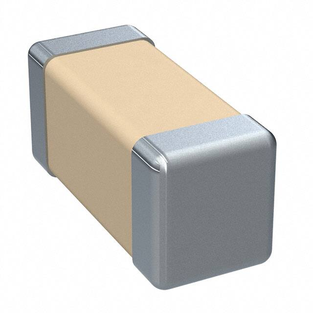


 工商网监
湘ICP备2023018690号
工商网监
湘ICP备2023018690号
