Surface Mount Multilayer Ceramic Capacitors
Commercial Grade
Surface Mount Multilayer Ceramic
Chip Capacitors
One world. One KEMET.
Electronic Components
�Surface Mount Multilayer Ceramic Chip Capacitors
Commercial Grade
Table of Contents Page
Why Choose KEMET......................................................................................................................................................... 4
Standard Products
C0G Dielectric, 10 – 200 VDC.......................................................................................................................................................6
X7R Dielectric, 6.3 – 250 VDC.....................................................................................................................................................16
X5R Dielectric, 4 – 50 VDC..........................................................................................................................................................28
Z5U Dielectric, 50 – 100 VDC......................................................................................................................................................37
Y5V Dielectric, 6.3 – 50 VDC.......................................................................................................................................................45
Capacitor Array, C0G Dielectric, 10 – 200 VDC...........................................................................................................................53
Capacitor Array, X7R Dielectric, 10 – 200 VDC...........................................................................................................................60
Commercial Off-the-Shelf (COTS) for Higher Reliability Applications, C0G Dielectric, 10 – 200 VDC........................................67
Commercial Off-the-Shelf (COTS) for Higher Reliability Applications, X7R Dielectric, 6.3 – 200 VDC.......................................76
Telecom “Tip and Ring” X7R Dielectric, 250 VDC.......................................................................................................................87
Flex Mitigation Solutions
Open Mode Design (FO-CAP), X7R Dielectric, 16 – 200 VDC....................................................................................................96
Floating Electrode Design (FE-CAP) X7R Dielectric, 6.3 – 250 VDC........................................................................................105
Flexible Termination System (FT-CAP) C0G Dielectric, 10 – 200 VDC..................................................................................... 114
Flexible Termination System (FT-CAP) X7R Dielectric, 6.3 – 250 VDC.....................................................................................123
High Voltage with Flexible Termination System (HV FT-CAP) X7R Dielectric, 500 – 3,000 VDC..............................................133
Flexible Termination System (FT-CAP), Ultra-Stable X8R Dielectric, 25 – 100 VDC (Commercial & Automotive Grade).........143
Floating Electrode Design with Flexible Termination System (FF-CAP) X7R Dielectric, 6.3 – 250 VDC................................... 151
KPS Series, X7R Dielectric, 10 – 250 VDC...............................................................................................................................160
KPS Series, High Voltage, X7R Dielectric, 500 – 630 VDC....................................................................................................... 171
KPS HT Series, High Temperature 150°C, X8L Dielectric, 10 VDC – 50 VDC..........................................................................178
SnPb End Metallization
Commercial “L” Series, SnPb Termination, C0G Dielectric, 10 – 200 VDC................................................................................185
Commercial “L” Series, SnPb Termination, X7R Dielectric, 6.3 – 250 VDC...............................................................................195
Commercial Off-the-Shelf (COTS) for Higher Reliability Applications, C0G Dielectric, 10 – 200 VDC......................................205
Commercial Off-the-Shelf (COTS) for Higher Reliability Applications, X7R Dielectric, 6.3 – 200 VDC.....................................214
High Temperature 150ºC, Ultra Stable X8R Dielectric, 25 – 100 VDC.......................................................................................225
High Temperature 150ºC, X8L Dielectric, 10 – 50 VDC.............................................................................................................233
Telecom “Tip and Ring,” X7R Dielectric, 250 VDC.....................................................................................................................242
Open Mode Design (FO-CAP), X7R Dielectric, 16 – 200 VDC..................................................................................................250
Floating Electrode Design (FE-CAP) X7R Dielectric, 6.3 – 250 VDC........................................................................................259
Flexible Termination System (FT-CAP) X7R Dielectric, 6.3 – 250 VDC.....................................................................................268
Floating Electrode Design with Flexible Termination System (FF-CAP) X7R Dielectric, 6.3 – 250 VDC...................................278
One world. One KEMET
© KEMET Electronics Corporation • P.O. Box 5928 • Greenville, SC 29606 (864) 963-6300 • www.kemet.com
CC101_COMM_SMD • 11/25/2013
2
�Bulk Capacitance Solutions (Stacked Capacitors)
KPS Series, X7R Dielectric, 10 – 250 VDC...............................................................................................................................287
KPS Series, High Voltage, X7R Dielectric, 500 – 630 VDC.......................................................................................................298
KPS HT Series, High Temperature 150°C, X8L Dielectric, 10 VDC – 50 VDC..........................................................................305
KEMET Power Solutions (KPS) MIL Series, Stacked Capacitors, 50 – 500 VDC..................................................................... 312
High Temperature
High Temperature 150ºC, Ultra Stable X8R Dielectric, 25 – 100 VDC.......................................................................................335
High Temperature 150ºC, X8L Dielectric, 10 – 50 VDC.............................................................................................................343
High Temperature 200ºC, C0G Dielectric, 10 – 200 VDC..........................................................................................................352
Flexible Termination System (FT-CAP), Ultra-Stable X8R Dielectric, 25 – 100 VDC (Commercial & Automotive Grade).........361
KPS HT Series, High Temperature 150°C, X8L Dielectric, 10 VDC – 50 VDC..........................................................................369
Pulse Detonation, High Voltage, High Temperature 200ºC, C0G Dielectric, 500 – 2,000 VDC (Industrial Grade)....................376
High Voltage
High Voltage C0G Dielectric, 500 – 3,000 VDC.........................................................................................................................383
High Voltage X7R Dielectric, 500 – 3,000 VDC.........................................................................................................................393
High Voltage with Flexible Termination System (HV FT-CAP), X7R Dielectric, 500 – 3,000 VDC.............................................404
ArcShield™ Technology, High Voltage, X7R Dielectric, 500 – 1,000 VDC (Commercial & Automotive Grade)......................... 414
KPS Series, High Voltage, X7R Dielectric, 500 – 630 VDC.......................................................................................................423
KPS HV, Large Case, SM Series, C0G Dielectric, 500 – 10,000 VDC (Industrial Grade).........................................................430
KPS HV, Large Case, SM Series, X7R Dielectric, 500 – 10,000 VDC (Industrial Grade)..........................................................440
Pulse Detonation, High Voltage, High Temperature 200ºC, C0G Dielectric, 500 – 2,000 VDC (Industrial Grade)....................451
Marking Information
Marking for X7R, COTS (X7R), SnPb (X7R), Tip & Ring (X7R), Open Mode (X7R), FE-CAP (X7R), FT-CAP (X7R), FF-CAP
(X7R), HV X7R, HV FT-CAP (X7R), HV X7R ARC SHIELD, X5R, AUTO (X5R), Z5U, X8L, Array X7R, KPS (X7R), and KPS
HV (X7R)....................................................................................................................................................................................458
Marking Information for C0G, 200°C C0G, COTS (C0G), SnPb (C0G), HV C0G, FT-CAP (C0G), FT-CAP (X8R), Y5V, X8R, HV/HT PULSE DETONATION (C0G),
and Array C0G is included within the appropriate product sections.
Packaging Information.................................................................................................................................................. 459
KPS Packaging Information......................................................................................................................................... 465
KEMET Corporation Sales Offices.............................................................................................................................. 470
Other KEMET Resources...............................................................................................................................................471
One world. One KEMET
© KEMET Electronics Corporation • P.O. Box 5928 • Greenville, SC 29606 (864) 963-6300 • www.kemet.com
CC101_COMM_SMD • 11/25/2013
3
�One world. One source. One KEMET.
When you partner with KEMET, our entire global organization provides you with the
coordinated service you need. No bouncing from supplier to supplier. No endless phone
calls and web browsing. We’re your single, integrated source for electronic component
solutions worldwide.
Less hassles. More solutions.
Our commitment to product quality and on-time delivery has helped customers
succeed for over 90 years. There’s a reason KEMET components can be found in
defense and aerospace equipment. Our reputation is built on a history of consistency,
reliability and service.
The “Easy-to-Buy-From” company.
KEMET offers a level of responsiveness that far surpasses any other supplier. Our
passion for customer service is evident throughout our global sales organization, which
offers localized support bolstered by our worldwide logistics capabilities. Whether you
need rush samples, technical assistance, in-person consultation, accelerated custom
design, design collaboration or prototype services, we have a solution.
OneOne
World.
world.One
OneKEMET
KEMET
©
Electronics Corporation
Corporation••P.O.
P.O. Box
Box5928
5928••Greenville,
Greenville,SC
SC29606
29606(864)
(864)963-6300
963-6300• www.kemet.com
• www.kemet.com
© KEMET
KEMET Electronics
CC101_COMM_SMD • 11/25/2013
4
�Made for you.
When you need custom products delivered on a tight schedule, you can trust KEMET.
Get direct design consultation from global experts, who help you get the job done on
time and within budget.
Working for a better world.
KEMET is dedicated to economically, environmentally and socially sustainable
development. We’ve adopted the Electronic Industry Code of Conduct (EICC) to
address all aspects of corporate responsibility. Our manufacturing facilities have won
numerous environmental excellence awards and recognitions, and our supply chain is
certified. We believe doing the right thing is in everyone’s interest.
About KEMET.
KEMET Corporation is a leading global supplier of electronic components. We offer
our customers the broadest selection of capacitor technologies in the industry across
multiple dielectrics, along with an expanding range of electromechanical devices, and
electromagnetic compatibility solutions. Our vision is to be the preferred supplier of
electronic component solutions for customers demanding the highest standards of
quality, delivery and service.
OneOne
World.
world.One
OneKEMET
KEMET
©
Electronics Corporation
Corporation••P.O.
P.O.Box
Box5928
5928••Greenville,
Greenville,SC
SC29606
29606(864)
(864)963-6300
963-6300• www.kemet.com
• www.kemet.com
© KEMET
KEMET Electronics
CC101_COMM_SMD • 11/25/2013
5
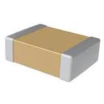
�Surface Mount Multilayer Ceramic Chip Capacitors (SMD MLCCs)
C0G Dielectric, 10 – 200 VDC (Commercial Grade)
Overview
KEMET’s C0G dielectric features a 125°C maximum operating
temperature and is considered “stable.” The Electronics
Components, Assemblies & Materials Association (EIA)
characterizes C0G dielectric as a Class I material. Components
of this classification are temperature compensating and are
suited for resonant circuit applications or those where Q and
stability of capacitance characteristics are required. C0G exhibits
no change in capacitance with respect to time and voltage and
boasts a negligible change in capacitance with reference to
ambient temperature. Capacitance change is limited to ±30
ppm/ºC from -55°C to +125°C.
Benefits
• -55°C to +125°C operating temperature range
• RoHS Compliant
• EIA 0201, 0402, 0603, 0805, 1206, 1210, 1808, 1812, 1825,
2220, and 2225 case sizes
• DC voltage ratings of 10 V, 16 V, 25 V, 50 V, 100 V, and 200 V
• Capacitance offerings ranging from 0.5 pF up to 0.47 μF
• Available capacitance tolerances of ±0.10 pF, ±0.25 pF, ±0.5
pF, ±1%, ±2%, ±5%, ±10%, and ±20%
• No piezoelectric noise
• Extremely low ESR and ESL
• High thermal stability
• High ripple current capability
• Preferred capacitance solution at line frequencies and into the
MHz range
• No capacitance change with respect to applied rated DC voltage
• Negligible capacitance change with respect to temperature from
-55°C to +125°C
• No capacitance decay with time
• Non-polar device, minimizing installation concerns
• 100% pure matte tin-plated termination finish allowing for
excellent solderability
• SnPb plated termination finish option available upon request (5%
minimum)
Ordering Information
C
Ceramic
1206
C
Case Size Specification/
(L" x W")
Series1
0201
0402
0603
0805
1206
1210
1808
1812
1825
2220
2225
C = Standard
104
J
3
G
Capacitance
Code (pF)
Capacitance
Tolerance2
Voltage
Dielectric
2 significant digits +
number of zeros.
Use 9 for 1.0 – 9.9 pF
Use 8 for 0.5 – .99 pF
e.g., 2.2 pF = 229
e.g., 0.5 pF = 508
B = ±0.10 pF
C = ±0.25 pF
D = ±0.5 pF
F = ±1%
G = ±2%
J = ±5%
K = ±10%
M = ±20%
8 = 10 V
4 = 16 V
3 = 25 V
5 = 50 V
1 = 100 V
2 = 200 V
G = C0G
A
C
TU
Packaging/Grade
Failure Rate/
Termination Finish3
(C-Spec)4
Design
Flexible termination option is available. Please see FT-CAP product bulletin C1062_C0G_FT-CAP_SMD
Additional capacitance tolerance offerings may be available. Contact KEMET for details.
3
Additional termination finish options may be available. Contact KEMET for details.
4
Additional reeling or packaging options may be available. Contact KEMET for details.
A = N/A
C = 100% Matte Sn Blank = Bulk
TU = 7" Reel
Unmarked
1
2
© KEMET Electronics Corporation • P.O. Box 5928 • Greenville, SC 29606 (864) 963-6300 • www.kemet.com
www.kemet.com
One world. One KEMET
CC101_COMM_SMD
C1003_C0G • 11/25/2013
61
�Surface Mount Multilayer Ceramic Chip Capacitors (SMD MLCCs) – C0G Dielectric, 10 – 200 VDC (Commercial Grade)
Dimensions – Millimeters (Inches)
100% Tin or SnPb Plate
L
W
B
T
Nickel Plate
S
Electrodes
Metric
Size
Code
B
Bandwidth
S
Separation
Minimum
0201
0603
0.60 (.024) ± 0.03 (.001) 0.30 (.012) ± 0.03 (.001)
0.15 (.006) ± 0.05 (.002)
N/A
0402
1005
1.00 (.040) ± 0.05 (.002) 0.50 (.020) ± 0.05 (.002)
0.30 (.012) ± 0.10 (.004)
0.30 (.012)
0603
1608
1.60 (.063) ± 0.15 (.006) 0.80 (.032) ± 0.15 (.006)
0.35 (.014) ± 0.15 (.006)
0.70 (.028)
0805
2012
2.00 (.079) ± 0.20 (.008) 1.25 (.049) ± 0.20 (.008)
0.50 (0.02) ± 0.25 (.010)
0.75 (.030)
1206
3216
3.20 (.126) ± 0.20 (.008) 1.60 (.063) ± 0.20 (.008)
1210
3225
1808
4520
0.50 (0.02) ± 0.25 (.010)
See Table 2 for
3.20 (.126) ± 0.20 (.008) 2.50 (.098) ± 0.20 (.008)
0.50 (0.02) ± 0.25 (.010)
Thickness
4.70 (.185) ± 0.50 (.020) 2.00 (.079) ± 0.20 (.008)
0.60 (.024) ± 0.35 (.014)
1812
4532
4.50 (.177) ± 0.30 (.012)
3.20 (.126) ± 0.30 (.012)
0.60 (.024) ± 0.35 (.014)
1825
4564
4.50 (.177) ± 0.30 (.012) 6.40 (.252) ± 0.40 (.016)
0.60 (.024) ± 0.35 (.014)
2220
5650
5.70 (.224) ± 0.40 (.016) 5.00 (.197) ± 0.40 (.016)
0.60 (.024) ± 0.35 (.014)
2225
5664
5.60 (.220) ± 0.40 (.016) 6.40 (.248) ± 0.40 (.016)
0.60 (.024) ± 0.35 (.014)
L
Length
W
Width
T
Thickness
Ceramic Surface Mount
EIA
Size
Code
Conductive Metalization
N/A
Mounting
Technique
Solder Reflow Only
Solder Wave or
Solder Reflow
Solder Reflow Only
Applications
Typical applications include critical timing, tuning, circuits requiring low loss, circuits with pulse, high current, decoupling, bypass,
filtering, transient voltage suppression, blocking and energy storage.
Qualification/Certification
Commercial Grade products are subject to internal qualification. Details regarding test methods and conditions are referenced in
Table 4, Performance and Reliability.
© KEMET Electronics Corporation • P.O. Box 5928 • Greenville, SC 29606 (864) 963-6300 • www.kemet.com
www.kemet.com
CC101_COMM_SMD
C1003_C0G • 11/25/2013
72
�Surface Mount Multilayer Ceramic Chip Capacitors (SMD MLCCs) – C0G Dielectric, 10 – 200 VDC (Commercial Grade)
Environmental Compliance
RoHS Compliant.
Electrical Parameters/Characteristics
Item
Parameters/Characteristics
Operating Temperature Range
Capacitance Change with Reference to +25°C and 0 VDC Applied (TCC)
Aging Rate (Maximum % Capacitance Loss/Decade Hour)
Dielectric Withstanding Voltage (DWV)
Dissipation Factor (DF) Maximum Limit @ 25ºC
Insulation Resistance (IR) Limit @ 25°C
-55°C to +125°C
±30 ppm/ºC
0%
250% of rated voltage
(5 ±1 seconds and charge/discharge not exceeding 50 mA)
0.1%
1,000 megohm microfarads or 100 GΩ
(Rated voltage applied for 120 ±5 seconds @ 25°C)
To obtain IR limit, divide MΩ-µF value by the capacitance and compare to GΩ limit. Select the lower of the two limits.
Capacitance and Dissipation Factor (DF) measured under the following conditions:
1 MHz ±100 kHz and 1.0 Vrms ±0.2 V if capacitance ≤ 1,000 pF
1 kHz ±50 Hz and 1.0 Vrms ±0.2 V if capacitance > 1,000 pF
Note: When measuring capacitance it is important to ensure the set voltage level is held constant. The HP4284 and Agilent E4980 have a feature known as
Automatic Level Control (ALC). The ALC feature should be switched to "ON."
Post Environmental Limits
High Temperature Life, Biased Humidity, Moisture Resistance
Dielectric
Rated DC
Voltage
Capacitance
Value
Dissipation Factor
(Maximum %)
C0G
All
All
0.5
Capacitance
Shift
Insulation
Resistance
0.3% or ±0.25 pF 10% of Initial Limit
© KEMET Electronics Corporation • P.O. Box 5928 • Greenville, SC 29606 (864) 963-6300 • www.kemet.com
www.kemet.com
CC101_COMM_SMD
C1003_C0G • 11/25/2013
83
�Surface Mount Multilayer Ceramic Chip Capacitors (SMD MLCCs) – C0G Dielectric, 10 – 200 VDC (Commercial Grade)
Table
Table 1A
1A –– Capacitance
Capacitance Range/Selection
Range/Selection Waterfall
Waterfall (0201
(0201 –– 1206
1206 Case
Case Sizes)
Sizes)
5
1
2
200
3
EB EB EB EB
EB EB EB EB
EB EB EB EB
EB EB EB EB
EB EB EB EB
EB EB EB EB
EB EB EB EB
EB EB EB EB
EB EB EB EB
EB EB EB EB
EB EB EB EB
EB EB EB EB
EB EB EB EB
EB EB EB EB
EB EB EB EB
EB EB EB EB
EB EB EB EB
EB EB EB EB
EB EB EB EB
EB EB EB EB
EB EB EB EB
EB EB EB EB
EB EB EB EB
EB EB EB EB
EB EB EB EB
EB EB EB EB
EB EB EB EB
EB EB EB EB
EB EB EB EB
EB EB EB EB
EB EB EB EB
EB EB EB EB
EB EB EB EB
EB EB EB EB
EB EB EB EB
EB EB EB EB
EB EB EB EB
EB EB EB EB
EB EB EB EB
EB EB EB EB
EB EB EB EB
EB EBTUEB EB
EB EB EB EB
Packaging/Grade
EB EB EB EB
EB (C-Spec)
EB EB EB
EB
EB= Bulk
EB EB
Blank
EB
EB EB
TU =EB7" Reel
EB EB EB EB
Unmarked
EB EB EB EB
EB EB EB EB
EB
EB
EB
EB
EB
EB
EB
EB
EB
EB
EB
EB
EB
EB
EB
EB
EB
EB
EB
EB
EB
EB
EB
EB
EB
EB
EB
EB
EB
EB
EB
EB
EB
EB
EB
EB
EB
EB
EB
EB
EB
EB
EB
EC
ED
ED
ED
ED
EE
EC
EB
EB
EB
EB
EB
EB
EB
EB
EB
EB
EB
EB
EB
EB
EB
EB
EB
EB
EB
EB
EB
EB
EB
EB
EB
EB
EB
EB
EB
EB
EB
EB
EB
EB
EB
EB
EB
EB
EB
EB
EB
EB
EB
EC
EC
ED
ED
ED
EE
EC
200
4
50
8
100
2
50
1
100
5
16
3
25
4
10
8
200
50
2
50
16
1
C1206C
100
5
16
3
25
4
10
8
100
2
C0805C
200
1
J K M AB¹ AB¹ AB¹
J K M
J K M AB² AB² AB²
J K M
J K M AB² AB² AB²
J K M
J K M AB² AB² AB²
J K M
J K M AB² AB² AB²
J K M
J K M AB² AB² AB²
J K M
J K M AB² AB² AB²
J K M
J K M AB² AB² AB²
J K M
J K M AB² AB² AB²
J K M
J K M AB² AB² AB²
J K M
J K M AB² AB² AB²
J K M
J K M AB² AB² AB²
J K M
J K M AB² AB² AB²
J K M
J K M
J K M
J K M
J K M
J K M
J K M
J K M
J K M
J K M
J K M
J K M
J K M
J K M
J K M
J K M104
J K M
Capacitance
J K M
J K Code
M (pF)
J2 signifi
K Mcant digits +
J number
K M of zeros.
J K M
Use 9 for 1.0 – 9.9 pF
J K M
Use 8 for 0.5 – .99 pF
J K M
BB BB BB BB
BB BB BB BB
BB BB BB BB
BB BB BB BB
BB BB BB BB
BB BB BB BB
BB BB BB BB
BB BB BB BB
BB BB BB BB
BB BB BB BB
BB BB BB BB
BB BB BB BB
BB BB BB BB
BB BB BB BB
BB BB BB BB
BB BB BB BB
BB BB BB BB
BB BB BB BB
BB BB BB BB
BB BB BB BB
BB BB BB BB
BB BB BB BB
BB BB BB BB
BB BB BB BB
BB BB BB BB
BB BB BB BB
BB BB BB BB
BB BB BB BB
BB BB BB BB
BB BB BB BB
BB BB BB BB
BB BB BB BB
BB BB BB BB
BB BB BB BB
BB BB BB BB
BB BB BB BB
BB BB BB BB
BB BB BB BB
BB BB BB BB
BB BB BB BB
BB BB BB BB
BB BB BB BB
BB BBJ BB BB
BB BB BB BB
Capacitance
BB BB BB BB
BBTolerance
BB BB BB
BB
BBpF
B = BB
±0.10
BB
BBpF
C =BB
±0.25
BB BB BB
D = ±0.5 pF
BB BB BB
CB
CB
CB
CB
CB
CB
CB
CB
CB
CB
CB
CB
CB
CB
CB
CB
CB
CB
CB
CB
CB
CB
CB
CB
CB
CB
BB BB CB
BB BB CB
BB BD CB
BB BD CB
BB
CB
BB
CB
BB
CB
BB
CB
BB
CB
BB
CB
BB
CB
BB
CB
BB
CB
BB
CB
BB
CB
BB
CB
3 CB
CB
Voltage CB
CB
8 = 10 V CB
4 = 16 V CB
CB
3 = 25 V
CB
5 = 50 V
CB
CB CB CB
CB CB CB
CB CB CB
CB CB CB
CB CB CB
CB CB CB
CB CB CB
CB CB CB
CB CB CB
CB CB CB
CB CB CB
CB CB CB
CB CB CB
CB CB CB
CB CB CB
CB CB CB
CB CB CB
CB CB CB
CB CB CB
CB CB CB
CB CB CB
CB CB CB
CB CB CB
CB CB CB
CB CB CB
CB CB CB
CB CB CF
CB CB CB
CB CB CB
CB CB CF
CB CB CB
CB CB CB
CB CB CB
CB CB CB
CB CB CB
CB CB CB
CB CB CB
CB CB CB
CB CB CB
CB CB CB
CB CB CB
CB CB CB
CB G
CB CB
CB CB CB
CB
CB CB
Dielectric
CB CB CB
CB
G = CB
C0GCB
CB CB CB
CB CB CB
CB CB CB
CB CB CB
25
Product
Availability
ChipThickness
Thickness
Codes
Product
Availabilityand
and Chip
Codes
See See
Table
2 for
Dimensions
Table
2 forChip
Chip Thickness
Thickness Dimensions
200
0.50 & 0.75 pF
508 & 758 B C D
1.0 - 9.1 pF*
109 - 919* B C D
10 pF
100
F G
11 pF
110
F G
12 pF
120
F G
13 pF
130
F G
15 pF
150
F G
16 pF
160
F G
18 pF
180
F G
20 pF
200
F G
22 pF
220
F G
24 pF
240
F G
27 pF
270
F G
30 pF
300
F G
33 pF
330
F G
36 pF
360
F G
39 pF
390
F G
43 pF
430
F G
47 pF
470
F G
51 pF
510
F G
56 pF
560
F G
62 pF
620
F G
68 pF
680
F G
75 pF
750
F G
82 pF
820
F G
91 pF
910
F G
100 pF
101
F G
110 - 270 pF*
111 - 271*
F G
300 pF
301
F G
330 pF
331
F G
360 pF
361
F G
390 pF
391
F G
430 pF
431
F G
470 pF
471
F G
510 pF
511
F G
560 pF
561
F G
620 pF
621
F G
680 pF
681
F G
750 pF
751
F G
820 pF
821
F G
910 pF
911
F G
1,000 pF
102
F G
C
1206
C F G
1,100 pF
112
1,200 pF
122
F G
Case Size
Specification/
1,300
pF
132
F G
Ceramic
(L" x W")
Series F G
1,500 pF
152
1,600 pF
162
F G
0201
C = Standard
1,800 pF
182
F G
0402
2,000 pF
202
F G
0603
2,200 pF
222
F G
0805
2,400 pF
242
F G
5
25
10
Capacitance
Capacitance
Tolerance
Tolerance
3
10
Rated Voltage (VDC)
4
100
8
C0603C
200
3
50
4
16
8
25
Voltage Code
25
C0402C
16
Cap
Code
C0201C
10
Capacitance
Case Size /
Series
CB CB DC
CB CB DC
CB CB DC
CB CB DC
CB CB DC
CB CB DC
CB CB DC
CB CB DC
CB CB DC
CB CB DC
CB CB DE
CB CB DC
CB CB DC
CB CB DC
CB CB DC
CB CB DC
CB CB DC
CB CB DC
CB CB DC
CB CB DC
CB CB DC
CB CB DC
CB CB DC
CB CB DC
CB CB DC
CB CB DC
CB CB DC
CB CB DC
CB CB DC
CB CB DC
CB CB DC
CB CB DC
CB CB DC
CB CB DC
CB CB DC
CB CB DC
CB CB DC
CB CB DC
CB CB DC
CB CB DC
CB CB DC
CB CB DC
A DC
CB CH
CB CH DC
Failure
Rate/
CB CH DD
Design
CB CH DD
CB
CH DD
A = N/A
CB CH DD
CB CH DC
CB CH DC
CB
DC
DC DC DC DC DC
DC DC DC DC DC
DC DC DC DC DC
DC DC DC DC DC
DC DC DC DC DC
DC DC DC DC DC
DC DC DC DC DC
DC DC DC DC DC
DC DC DC DC DC
DC DC DC DC DC
DE DE DE DC DC
DC DC DC DC DC
DC DC DC DC DC
DC DC DC DC DC
DC DC DC DC DC
DC DC DC DC DC
DC DC DC DC DC
DC DC DC DC DC
DC DC DC DC DC
DC DC DC DC DC
DC DC DC DC DC
DC DC DC DC DC
DC DC DC DC DC
DC DC DC DC DC
DC DC DC DC DC
DC DC DC DC DC
DC DC DC DC DC
DC DC DC DC DC
DC DC DC DC DC
DC DC DC DC DC
DC DC DC DC DC
DC DC DC DC DC
DC DC DC DC DC
DC DC DC DC DD
DC DC DC DC DC
DC DC DC DC DC
DC DC DC DC DC
DC DC DC DC DC
DC DC DC DC DC
DC DC DC DC DC
DC DC DC DD DD
DC DC DC DD DD
C DC DC
DC DC DC
DC DC DC DC DC
DD
DD DD Finish
DD DC
Termination
DD DD DD DD DC
DD
DDMatte
DD Sn
DC
C =DD
100%
DD DD DD DD DC
DC DC DC DC DC
DC DC DC DC DC
DC DC DC DC DC
25
16
10
200
100
50
16
25
10
100
200
50
16
10
100
50
16
25
10
25
16
10
F = ±1%
1206
e.g., 2.2 pF = 229
G = ±2%
1 = 100 V
Rated Voltage (VDC)
1210
e.g., 0.5 pF = 508
J = ±5%
2 = 200 V
Cap
1808
Voltage Code
8 4 3 8K = ±10%
4 3 5 1 2 8 4 3 5 1 2 8 4 3 5 1 2 8 4 3 5 1
Capacitance
Capacitance
Cap
Code
Code
1812
M = ±20%
Case
Series C0201C
C0402C
C0603C
C0805C
C1206C
CaseSize
Size // Series
C0201C
C0402C
C0603C
C0805C
C1206C
1825
2220
2225
*Capacitance range Includes
E24 decade values only. (i.e., 10, 11, 12, 13, 15, 16, 18, 20, 22, 24, 27, 30, 33, 36, 39, 43, 47, 51, 56, 62, 68, 75, 82 and 91).
2
xx¹ Available only in D, J, K,M tolerance
xx² Available only in J, K, M tolerance.
These products are protected under US Patents 7,172,985 & 7,670,981, other patents pending, and any foreign counterparts.
© KEMET Electronics Corporation • P.O. Box 5928 • Greenville, SC 29606 (864) 963-6300 • www.kemet.com
www.kemet.com
Roll Over for
Order Info.
CC101_COMM_SMD
C1003_C0G • 11/25/2013
94
�Surface Mount Multilayer Ceramic Chip Capacitors (SMD MLCCs) – C0G Dielectric, 10 – 200 VDC (Commercial Grade)
Table 1A – Capacitance Range/Selection Waterfall (0201 – 1206 Case Sizes) cont'd
2
10
16
25
50
100
200
10
16
25
50
100
200
200
1
DC
DD
DD
DD
DE
DE
DE
DE
DC
DC
DC
DC
DC
DC
DC
DC
DC
DC
DD
DF
DG
DG
DG
DC
DD
DD
DD
DE
DE
DE
DE
DC
DC
DC
DC
DC
DC
DC
DC
DC
DC
DD
DF
DG
DG
DG
DC
DD
DD
DD
DE
DE
DE
DE
DC
DC
DC
DC
DC
DC
DC
DC
DC
DC
DD
DF
DG
DG
DG
DC
DD
DD
DD
DE
DE
DE
DE
DC
DC
DC
DC
DC
DC
DC
DC
DD
DD
DF
DC
DC
DC
DC
DC
DC
DC
DC
DC
DC
DC
DC
DC
DC
DD
DE
DG
DC
DC
DC
DD
DD
DD
DD
DD
DD
DG
DG
DG
DG
EB
EC
EC
EC
EC
EC
EC
ED
ED
EB
EB
EB
EC
EC
ED
EB
EB
EB
EB
EB
EB
EC
EC
ED
EF
EH
EH
EB
EC
EC
EC
EC
EC
EC
ED
ED
EB
EB
EB
EC
EC
ED
EB
EB
EB
EB
EB
EB
EC
EC
ED
EF
EH
EH
EB
EC
EC
EC
EC
EC
EC
ED
ED
EB
EB
EB
EC
EC
ED
EB
EB
EB
EB
EB
EB
EC
EC
ED
EF
EH
EH
EB
EC
EC
EC
EC
EC
EC
ED
ED
EB
EB
EB
EC
EC
ED
EB
EB
EB
EB
EB
EB
EE
EE
EF
EH
EH
EC
EC
EE
EE
EF
EC
EC
ED
ED
EB
EB
EB
EB
EB
EB
EB
EB
EB
EC
EE
EE
EH
EH
EC
200
5
50
3
100
4
50
8
100
2
16
1
25
5
25
3
10
4
16
8
10
2
200
1
50
5
100
3
25
4
16
8
10
2
200
1
100
50
C1206C
2
8
4
3
5
1
2
8
4
3
5
1
2
8
C0201C
4
3
5
1
2
CB
CB
CB
CB
CB
CB
CB
50
3
CB
CB
CB
CB
CB
CB
CB
CB
CB
CB
CB
100
4
CB
CB
CB
CB
CB
CB
CB
CB
CB
CB
CB
CB
CB
CB
CB
CB
CB
25
8
CB
CB
CB
CB
CB
CB
CB
CB
CB
CB
CB
CB
CB
CB
CB
CB
CB
16
Voltage Code
100
Rated Voltage (VDC)
CB
CB
CB
CB
CB
CB
CB
CB
CB
CB
CB
CB
CB
CB
CB
CB
CB
10
Product Availability and Chip Thickness Codes
See Table 2 for Chip Thickness Dimensions
M
M
M
M
M
M
M
M
M
M
M
M
M
M
M
M
M
M
M
M
M
M
M
M
M
M
M
Case Size / Series
C0805C
200
16
10
25
16
5
200
K
K
K
K
K
K
K
K
K
K
K
K
K
K
K
K
K
K
K
K
K
K
K
K
K
K
K
3
50
J
J
J
J
J
J
J
J
J
J
J
J
J
J
J
J
J
J
J
J
J
J
J
J
J
J
J
4
16
G
G
G
G
G
G
G
G
G
G
G
G
G
G
G
G
G
G
G
G
G
G
G
G
G
G
G
8
C0603C
25
F
F
F
F
F
F
F
F
F
F
F
F
F
F
F
F
F
F
F
F
F
F
F
F
F
F
F
3
25
10
Capacitance
Tolerance
4
10
Capacitance
Cap
Code
8
16
272
302
332
362
392
432
472
512
562
622
682
752
822
912
103
123
153
183
223
273
333
393
473
563
683
823
104
Voltage Code
Rated Voltage (VDC)
C0402C
25
2,700 pF
3,000 pF
3,300 pF
3,600 pF
3,900 pF
4,300 pF
4,700 pF
5,100 pF
5,600 pF
6,200 pF
6,800 pF
7,500 pF
8,200 pF
9,100 pF
10,000 pF
12,000 pF
15,000 pF
18,000 pF
22,000 pF
27,000 pF
33,000 pF
39,000 pF
47,000 pF
56,000 pF
68,000 pF
82,000 pF
0.10 µF
C0201C
10
Capacitance
Cap
Code
Case Size /
Series
8
4
3
5
1
C0402C
C0603C
C0805C
EB
EB
EB
EB
EB
EB
EB
EB
EB
EB
EB
EC
EC
EC
ED
EF
EH
EH
C1206C
*Capacitance range Includes E24 decade values only. (i.e., 10, 11, 12, 13, 15, 16, 18, 20, 22, 24, 27, 30, 33, 36, 39, 43, 47, 51, 56, 62, 68, 75, 82 and 91).
xx¹ Available only in D, J, K,M tolerance
xx² Available only in J, K, M tolerance.
These products are protected under US Patents 7,172,985 & 7,670,981, other patents pending, and any foreign counterparts.
C
Ceramic
1206
C
Case Size Specification/
(L" x W")
Series
0201
0402
0603
0805
1206
1210
1808
1812
1825
2220
2225
C = Standard
104
J
3
G
Capacitance
Code (pF)
Capacitance
Tolerance
Voltage
Dielectric
2 significant digits +
number of zeros.
Use 9 for 1.0 – 9.9 pF
Use 8 for 0.5 – .99 pF
e.g., 2.2 pF = 229
e.g., 0.5 pF = 508
B = ±0.10 pF
C = ±0.25 pF
D = ±0.5 pF
F = ±1%
G = ±2%
J = ±5%
K = ±10%
M = ±20%
8 = 10 V
4 = 16 V
3 = 25 V
5 = 50 V
1 = 100 V
2 = 200 V
G = C0G
A
TU
Failure Rate/
Packaging/Grade
Termination Finish
Design
(C-Spec)
A = N/A
© KEMET Electronics Corporation • P.O. Box 5928 • Greenville, SC 29606 (864) 963-6300 • www.kemet.com
www.kemet.com
Roll Over for
Order Info.
C
C = 100% Matte Sn Blank = Bulk
TU = 7" Reel
Unmarked
CC101_COMM_SMD
C1003_C0G • 11/25/2013
105
�Surface Mount Multilayer Ceramic Chip Capacitors (SMD MLCCs) – C0G Dielectric, 10 – 200 VDC (Commercial Grade)
Table 1B – Capacitance Range/Selection Waterfall (1210 – 2225 Case Sizes)
J
J
J
J
J
J
J
J
J
J
J
J
J
J
J
J
J
J
J
J
J
J
J
J
J
J
J
J
J
J
J
J
J
J
J
J
J
J
J
J
J
J
J
J
J
J
J
J
J
2
5
1
2
100
100
200
200
1
50
50
5
200
200
2
100
100
1
50
50
100
100
5
200
200
50
50
2
C2220C
C2225C
5
1
2
200
200
F G
F G
F G
F G
F G
F G
F G
F G
F G
F G
F G
F G
F G
F G
F G
F G
F G
F G
F G
F G
F G
F G
F G
F G
F G
F G
F G
F G
F G
F G
F G
F G
F G
F G
F G
F G
F G
F G
F G
F G
F G
F G
F G
C F G
F G
F G
Specification/
SeriesF G
F G
C = Standard
F G
1
C1825C
100
100
B C D
B C D
5
100
100
25
25
Capacitance
Capacitance
Tolerance
Tolerance
2
50
50
1
C1812C
200
200
5
100
100
3
50
50
4
200
200
8
16
16
C1808C
50
50
0.5 & 0.75 pF
508 & 758
1.0 - 9.1 pF*
109 - 919*
10 - 91 pF*
100 - 910*
100 - 300 pF*
101 - 301*
330 - 430 pF*
331 - 431*
470 - 910 pF*
471 - 911*
1,000 pF
102
1,100 pF
112
1,200 pF
122
1,300 pF
132
1,500 pF
152
1,600 pF
162
1,800 pF
182
2,000 pF
202
2,200 pF
222
2,400 pF
242
2,700 pF
272
3,000 pF
302
3,300 pF
332
3,600 pF
362
3,900 pF
392
4,300 pF
432
4,700 pF
472
5,100 pF
512
5,600 pF
562
6,200 pF
622
6,800 pF
682
7,500 pF
752
8,200 pF
822
9,100 pF
912
10,000 pF
103
12,000 pF
123
15,000 pF
153
18,000 pF
183
22,000 pF
223
27,000 pF
273
33,000 pF
333
39,000 pF
393
47,000 pF
473
56,000 pF
563
68,000 pF
683
82,000 pF
823
0.10 µF
104
0.12 µF
124
0.15 µF
154
0.18 µFC
184
1206
0.22 µF
224
0.27 µF
Case274
Size
0.33Ceramic
µF
(L" x334
W")
0.39 µF
394
0201
0.47 µF
474
Voltage Code
Rated Voltage (VDC)
C1210C
10
10
Cap
Capacitance
Code
Case Size /
Series
KE
KE
KE
KE
KE
KE
KE
KE
KE
KE
KE
KE
KE
KE
KE
KE
KE
KE
KE
KE
KE
KE
KE
KE
KE
KE
KE
KE
KE
KE
KE
KE
KE
KE
KE
KE
KE
KE
KE
KE
Product
Availability
ChipThickness
Thickness
Codes
Product
Availabilityand
and Chip
Codes
See See
Table
2 for
Dimensions
Table
2 forChip
Chip Thickness
Thickness Dimensions
FB FB FB FB FB FB
K M FB FB FB FB FB FB
K M FB FB FB FB FB FB
K M FB FB FB FB FB FB
LF
LF
K M FB FB FB FB FB FB
LF
LF
K M FB FB FB FB FB FB
LF
LF
K M FB FB FB FB FB FB
LF
LF
K M FB FB FB FB FB FB
LF
LF
K M FB FB FB FB FB FC LF
LF
K M FB FB FB FB FB FE
LF
LF
K M FB FB FB FB FB FE
LF
LF
K M FB FB FB FB FB FE
LF
LF
K M FB FB FB FB FC FE
LF
LF
K M FB FB FB FB FC FG LF
LF
K M FB FB FB FB FC FC LF
LF
K M FB FB FB FB FC FC LF
LF
K M FB FB FB FB FC FF
LF
LF
K M FB FB FB FB FF
FF
LF
LF
K M FB FB FB FB FF
FF
LF
LF
K M FB FB FB FB FF
FF
LF
LF
K M FB FB FB FB FF
FF
LF
LF
K M FF
FF
FF
FF FG FG LF
LF
K M FB FB
FB FB FG FG
K M FB FB FB FB FG FG
K M FB FB FB FB FG FB
K M FB FB FB FB FG FB
K M FC FC FC FC FC FB
K M FC FC FC FC FC FB
K M FE FE FE FE FE FB
K M FF
FF
FF
FF
FF FB
K M FG FG FG FG FB FB
K M FG FG FG FG FB FC
K M FB FB FB FB FB FC
K M FB FB FB FB FB FF
K M FB FB FB FB FB FG
K M FB FB FB FB FB FH
K M FB FB FB FB FE FH
K M FB FB FB FB FE
FJ
K M FB FB FB FB FF
K M FB FB FB FC FG
K M FC FC FC FF FH
K M FE FE FE FG FM
K M FG FG FG FH
K M FH FH FH FM
K M 104
FJ
FJ
FJ
J
3
K M FK FK FK
K Capacitance
M
Capacitance
Voltage
K MCode (pF)
Tolerance
K M
2Ksignifi
B = ±0.10 pF
8 = 10 V
M cant digits +
LF
LF
LF
LF
LF
LF
LF
LF
LF
LF
LF
LF
LF
GB
GB
GB
GB
GB
GB
GB
GB
GB
GB
GB
GB
GB
GB
GB
GB
GB
GB
GB
GB
GB
GB
GB
GB
GB
GB
GB
GB
GB
GB
GB
GB
GB
GB
GB
GB
GB
GB
GB
HB
HB
HB
GB
GB
GD
HB
HB
HB
GB
GB
GH
HB
HB
HB
GB
GB
GJ
HB
HB
HB
JE
JE
JB
GB
GH
GB
HB
HB
HB
JE
JE
JB
GB
GB
GB
GB
GB
GB
GB
GB
GB
GB
GB
GB
GB
GB
GD
GGH
GK
GH
GG
GB
GB
GB
GB
GB
GB
GB
GB
GB
GB
GD
GH
GN
GB
GB
GB
GB
GB
GB
GB
GB
GD
GD
GK
GM
GM
HB
HB
HB
HB
HB
HB
HB
HB
HB
HE
HE
HG
HE
HE
Dielectric
A
Failure Rate/
Design
JE
JE
JB
JE
JB
JE
JE
JE
JB
JE
JE
JB
JE
JB
JB
JE
JB
JB
JB
JB
JB
JB
JB
JB
JB
JB
JB
JB
JB
JB
JB
JB
JB
JB
JB
JB
JB
JB
JD
JB
JB
JD
JB
JB JG
C JB JD JGTU
JB
JD
JL
JB
JF
Packaging/Grade
Termination Finish
JD JG (C-Spec)
JG
C = 100% Matte
JG Sn Blank = Bulk
Roll Over for
Order Info.
200
200
50
50
200
200
100
100
116
50
50
200
200
CC101_COMM_SMD
C1003_C0G • 11/25/2013
100
100
50
50
100
100
© KEMET Electronics Corporation • P.O. Box 5928 • Greenville, SC 29606 (864) 963-6300 • www.kemet.com
www.kemet.com
200
200
100
100
50
50
200
200
100
100
50
50
200
200
100
100
50
50
25
25
16
16
10
10
G = C0G
A = N/A
0402
number of zeros.
C = ±0.25 pF 4 = 16 V
TU = 7" Reel
Rated Voltage (VDC)
0603
Use
9
for
1.0
–
9.9
pF
D
=
±0.5
pF
3
=
25
V
Unmarked
Cap
Voltage Code
4 pF3 F =5 ±1%1
2 5 =550 V 1
2
5
1
2
5
1
2
5
1
2
5
1
2
Capacitance
Cap
Code
Capacitance
0805
Use 8 for 80.5 – .99
Code
1206
e.g., 2.2 pF = 229 C1210C
G = ±2%
1 = 100
V
CaseSize
Size // Series
C1210C
C1808C
C1812C
C1825C
C2220C
C2225C
Case
Series
C1808C
C1812C
C1825C
C2220C
C2225C
1210
e.g., 0.5 pF = 508
J = ±5%
2 = 200 V
1808
K =13,
±10%
*Capacitance range Includes
E24 decade values only. (i.e., 10, 11, 12,
15, 16, 18, 20, 22, 24, 27, 30, 33, 36, 39, 43, 47, 51, 56, 62, 68, 75, 82 and 91).
1812
M = ±20%
These products are protected
under US Patents 7,172,985 & 7,670,981, other patents pending, and any foreign counterparts.
1825
2220
2225
�Surface Mount Multilayer Ceramic Chip Capacitors (SMD MLCCs) – C0G Dielectric, 10 – 200 VDC (Commercial Grade)
Table 2 – Chip Thickness/Packaging Quantities
Paper Quantity
Plastic Quantity
Thickness
Code
Case
Size
Thickness ±
Range (mm)
7" Reel
13" Reel
7" Reel
13" Reel
AB
BB
BD
CB
CF
CH
DE
DC
DD
DF
DG
EB
EC
ED
EE
EF
EH
FB
FC
FE
FF
FG
FH
FM
FJ
FK
NC
LF
GB
GD
GH
GG
GK
GJ
GN
GM
HB
HE
HG
JB
JD
JE
JF
JG
JL
KE
0201
0402
0402
0603
0603
0603
0805
0805
0805
0805
0805
1206
1206
1206
1206
1206
1206
1210
1210
1210
1210
1210
1210
1210
1210
1210
1706
1808
1812
1812
1812
1812
1812
1812
1812
1812
1825
1825
1825
2220
2220
2220
2220
2220
2220
2225
0.30 ± 0.03
0.50 ± 0.05
0.55 ± 0.05
0.80 ± 0.07
0.80 ± 0.07
0.85 ± 0.07
0.70 ± 0.20
0.78 ± 0.10
0.90 ± 0.10
1.10 ± 0.10
1.25 ± 0.15
0.78 ± 0.10
0.90 ± 0.10
1.00 ± 0.10
1.10 ± 0.10
1.20 ± 0.15
1.60 ± 0.20
0.78 ± 0.10
0.90 ± 0.10
1.00 ± 0.10
1.10 ± 0.10
1.25 ± 0.15
1.55 ± 0.15
1.70 ± 0.20
1.85 ± 0.20
2.10 ± 0.20
1.00 ± 0.15
1.00 ± 0.15
1.00 ± 0.10
1.25 ± 0.15
1.40 ± 0.15
1.55 ± 0.10
1.60 ± 0.20
1.70 ± 0.15
1.70 ± 0.20
2.00 ± 0.20
1.10 ± 0.15
1.40 ± 0.15
1.60 ± 0.20
1.00 ± 0.15
1.30 ± 0.15
1.40 ± 0.15
1.50 ± 0.15
1.70 ± 0.15
2.00 ± 0.20
1.40 ± 0.15
15,000
10,000
10,000
4,000
4,000
4,000
4,000
4,000
4,000
0
0
4,000
0
0
0
0
0
0
0
0
0
0
0
0
0
0
0
0
0
0
0
0
0
0
0
0
0
0
0
0
0
0
0
0
0
0
0
50,000
50,000
10,000
15,000
10,000
10,000
10,000
10,000
0
0
10,000
0
0
0
0
0
0
0
0
0
0
0
0
0
0
0
0
0
0
0
0
0
0
0
0
0
0
0
0
0
0
0
0
0
0
0
0
0
0
0
0
0
0
0
2,500
2,500
4,000
4,000
2,500
2,500
2,500
2,000
4,000
4,000
2,500
2,500
2,500
2,000
2,000
2,000
2,000
4,000
2,500
1,000
1,000
1,000
1,000
1,000
1,000
1,000
500
1,000
1,000
1,000
1,000
1,000
1,000
1,000
1,000
500
1,000
0
0
0
0
0
0
0
0
0
10,000
10,000
10,000
10,000
10,000
10,000
10,000
8,000
10,000
10,000
10,000
10,000
10,000
8,000
8,000
8,000
8,000
10,000
10,000
4,000
4,000
4,000
4,000
4,000
4,000
4,000
2,000
4,000
4,000
4,000
4,000
4,000
4,000
4,000
4,000
2,000
4,000
Thickness
Code
Case
Size
Thickness ±
Range (mm)
7" Reel
13" Reel
7" Reel
13" Reel
Paper Quantity
Plastic Quantity
Package quantity based on finished chip thickness specifications.
© KEMET Electronics Corporation • P.O. Box 5928 • Greenville, SC 29606 (864) 963-6300 • www.kemet.com
www.kemet.com
CC101_COMM_SMD
C1003_C0G • 11/25/2013
127
�Surface Mount Multilayer Ceramic Chip Capacitors (SMD MLCCs) – C0G Dielectric, 10 – 200 VDC (Commercial Grade)
Table 3 – Chip Capacitor Land Pattern Design Recommendations per IPC–7351
EIA
Size
Code
Metric
Size
Code
0201
Density Level A:
Maximum (Most)
Land Protrusion (mm)
Density Level B:
Median (Nominal)
Land Protrusion (mm)
Density Level C:
Minimum (Least)
Land Protrusion (mm)
C
Y
X
V1
V2
C
Y
X
V1
V2
C
Y
X
V1
V2
0603
0.38
0.56
0.52
1.80
1.00
0.33
0.46
0.42
1.50
0.80
0.28
0.36
0.32
1.20
0.60
0402
1005
0.50
0.72
0.72
2.20
1.20
0.45
0.62
0.62
1.90
1.00
0.40
0.52
0.52
1.60
0.80
0603
1608
0.90
1.15
1.10
4.00
2.10
0.80
0.95
1.00
3.10
1.50
0.60
0.75
0.90
2.40
1.20
0805
2012
1.00
1.35
1.55
4.40
2.60
0.90
1.15
1.45
3.50
2.00
0.75
0.95
1.35
2.80
1.70
1206
3216
1.60
1.35
1.90
5.60
2.90
1.50
1.15
1.80
4.70
2.30
1.40
0.95
1.70
4.00
2.00
1210
3225
1.60
1.35
2.80
5.65
3.80
1.50
1.15
2.70
4.70
3.20
1.40
0.95
2.60
4.00
2.90
12101
3225
1.50
1.60
2.90
5.60
3.90
1.40
1.40
2.80
4.70
3.30
1.30
1.20
2.70
4.00
3.00
1808
4520
2.30
1.75
2.30
7.40
3.30
2.20
1.55
2.20
6.50
2.70
2.10
1.35
2.10
5.80
2.40
1812
4532
2.15
1.60
3.60
6.90
4.60
2.05
1.40
3.50
6.00
4.00
1.95
1.20
3.40
5.30
3.70
1825
4564
2.15
1.60
6.90
6.90
7.90
2.05
1.40
6.80
6.00
7.30
1.95
1.20
6.70
5.30
7.00
2220
5650
2.75
1.70
5.50
8.20
6.50
2.65
1.50
5.40
7.30
5.90
2.55
1.30
5.30
6.60
5.60
2225
5664
2.70
1.70
6.90
8.10
7.90
2.60
1.50
6.80
7.20
7.30
2.50
1.30
6.70
6.50
7.00
1
Only for capacitance values ≥ 22 µF
Density Level A: For low-density product applications. Recommended for wave solder applications and provides a wider process window for reflow solder
processes. KEMET only recommends wave soldering of EIA 0603, 0805 and 1206 case sizes.
Density Level B: For products with a moderate level of component density. Provides a robust solder attachment condition for reflow solder processes.
Density Level C: For high component density product applications. Before adapting the minimum land pattern variations the user should perform qualification
testing based on the conditions outlined in IPC Standard 7351 (IPC–7351).
Soldering Process
Recommended Soldering Technique:
• Solder wave or solder reflow for EIA case sizes 0603, 0805 and 1206
• All other EIA case sizes are limited to solder reflow only
Recommended Soldering Profile:
• KEMET recommends following the guidelines outlined in IPC/JEDEC J–STD–020
© KEMET Electronics Corporation • P.O. Box 5928 • Greenville, SC 29606 (864) 963-6300 • www.kemet.com
www.kemet.com
CC101_COMM_SMD
C1003_C0G • 11/25/2013
138
�Surface Mount Multilayer Ceramic Chip Capacitors (SMD MLCCs) – C0G Dielectric, 10 – 200 VDC (Commercial Grade)
Table 4 – Performance & Reliability: Test Methods and Conditions
Stress
Reference
Test or Inspection Method
Terminal Strength
JIS–C–6429
Appendix 1, Note: Force of 1.8 kg for 60 seconds.
Board Flex
JIS–C–6429
Appendix 2, Note: Standard termination system – 2.0 mm (minimum) for all except 3 mm for C0G.
Flexible termination system – 3.0 mm (minimum).
Magnification 50 X. Conditions:
Solderability
J–STD–002
a) Method B, 4 hours @ 155°C, dry heat @ 235°C
b) Method B @ 215°C category 3
c) Method D, category 3 @ 260°C
Temperature Cycling
JESD22 Method JA–104
Biased Humidity
MIL–STD–202 Method 103
Moisture Resistance
MIL–STD–202 Method 106
1,000 Cycles (-55°C to +125°C). Measurement at 24 hours +/- 2 hours after test conclusion.
Load Humidity: 1,000 hours 85°C/85% RH and rated voltage. Add 100 K ohm resistor. Measurement
at 24 hours +/- 2 hours after test conclusion.
Low Volt Humidity: 1,000 hours 85°C/85% RH and 1.5 V. Add 100 K ohm resistor.
Measurement at 24 hours +/- 2 hours after test conclusion.
t = 24 hours/cycle. Steps 7a and 7b not required. Unpowered.
Measurement at 24 hours +/- 2 hours after test conclusion.
-55°C/+125°C. Note: Number of cycles required – 300, maximum transfer time – 20 seconds, dwell
time – 15 minutes. Air – Air.
Thermal Shock
MIL–STD–202 Method 107
High Temperature Life
MIL–STD–202 Method 108
/EIA–198
Storage Life
MIL–STD–202 Method 108
150°C, 0 VDC for 1,000 hours.
Vibration
MIL–STD–202 Method 204
5 g's for 20 min., 12 cycles each of 3 orientations. Note: Use 8" X 5" PCB 0.031" thick 7 secure
points on one long side and 2 secure points at corners of opposite sides. Parts mounted within 2"
from any secure point. Test from 10 – 2,000 Hz
Mechanical Shock
MIL–STD–202 Method 213
Figure 1 of Method 213, Condition F.
Resistance to Solvents
MIL–STD–202 Method 215
Add aqueous wash chemical, OKEM Clean or equivalent.
1,000 hours at 125°C (85°C for X5R, Z5U and Y5V) with 2 X rated voltage applied.
Storage and Handling
Ceramic chip capacitors should be stored in normal working environments. While the chips themselves are quite robust in other
environments, solderability will be degraded by exposure to high temperatures, high humidity, corrosive atmospheres, and long term
storage. In addition, packaging materials will be degraded by high temperature– reels may soften or warp and tape peel force may
increase. KEMET recommends that maximum storage temperature not exceed 40ºC and maximum storage humidity not exceed 70%
relative humidity. Temperature fluctuations should be minimized to avoid condensation on the parts and atmospheres should be free of
chlorine and sulfur bearing compounds. For optimized solderability chip stock should be used promptly, preferably within 1.5 years of
receipt.
© KEMET Electronics Corporation • P.O. Box 5928 • Greenville, SC 29606 (864) 963-6300 • www.kemet.com
www.kemet.com
CC101_COMM_SMD
C1003_C0G • 11/25/2013
149
�Surface Mount Multilayer Ceramic Chip Capacitors (SMD MLCCs) – C0G Dielectric, 10 – 200 VDC (Commercial Grade)
Construction
Reference
Item
A
B
C
Termination
System
Material
Finish
100% Matte Sn
Barrier Layer
Ni
Base Metal
Cu
D
Inner Electrode
Ni
E
Dielectric Material
CaZrO3
Note: Image is exaggerated in order to clearly identify all components of construction.
Capacitor Marking (Optional):
Laser marking option is not available on:
•
•
•
•
C0G, Ultra Stable X8R and Y5V dielectric devices
EIA 0402 case size devices
EIA 0603 case size devices with Flexible Termination option.
KPS Commercial and Automotive grade stacked devices.
These capacitors are supplied unmarked only.
© KEMET Electronics Corporation • P.O. Box 5928 • Greenville, SC 29606 (864) 963-6300 • www.kemet.com
www.kemet.com
CC101_COMM_SMD
C1003_C0G • 11/25/2013
15
10
�Surface Mount Multilayer Ceramic Chip Capacitors (SMD MLCCs)
X7R Dielectric, 6.3 – 250 VDC (Commercial Grade)
Overview
KEMET’s X7R dielectric features a 125°C maximum operating
temperature and is considered “temperature stable.” The
Electronics Components, Assemblies & Materials Association
(EIA) characterizes X7R dielectric as a Class II material.
Components of this classification are fixed, ceramic dielectric
capacitors suited for bypass and decoupling applications
or for frequency discriminating circuits where Q and stability
of capacitance characteristics are not critical. X7R exhibits a
predictable change in capacitance with respect to time and voltage
and boasts a minimal change in capacitance with reference to
ambient temperature. Capacitance change is limited to ±15% from
-55°C to +125°C.
Benefits
Applications
•
•
•
•
Typical applications include decoupling, bypass, filtering and
transient voltage suppression.
•
•
•
•
•
•
-55°C to +125°C operating temperature range
Pb-Free and RoHS Compliant
Temperature stable dielectric
EIA 0402, 0603, 0805, 1206, 1210, 1808, 1812, 1825, 2220,
and 2225 case sizes
DC voltage ratings of 6.3 V, 10 V, 16 V, 25 V, 50 V, 100 V,
200 V, and 250 V
Capacitance offerings ranging from 10 pF to 47 μF
Available capacitance tolerances of ±5%, ±10%, and ±20%
Non-polar device, minimizing installation concerns
100% pure matte tin-plated termination finish allowing for
excellent solderability
SnPb termination finish option available upon request
(5% minimum)
Ordering Information
C
1206
C
106
M
4
R
Ceramic
Case Size
(L" x W")
Specification/
Series1
Capacitance
Code (pF)
Capacitance
Tolerance
Voltage
Dielectric
0402
0603
0805
1206
1210
1808
1812
1825
2220
2225
C = Standard
2 Significant
Digits + Number
of Zeros
J = ±5%
K = ±10%
M = ±20%
9 = 6.3 V
8 = 10 V
4 = 16 V
3 = 25 V
6 = 35 V
5 = 50 V
1 = 100 V
2 = 200 V
A = 250 V
R = X7R
A
C
TU
Failure Rate/
Termination Finish2
Design
A = N/A
C = 100% Matte Sn
Packaging/Grade
(C-Spec)3
Blank = Bulk
TU = 7" Reel
Unmarked
TM = 7" Reel
Marked
Flexible termination option is available. Please see FT-CAP product bulletin C1013_X7R_FT-CAP_SMD.
Additional termination finish options may be available. Contact KEMET for details.
3
Additional reeling or packaging options may be available. Contact KEMET for details.
1
2
One world. One KEMET
© KEMET Electronics Corporation • P.O. Box 5928 • Greenville, SC 29606 (864) 963-6300 • www.kemet.com
www.kemet.com
CC101_COMM_SMD
C1002_X7R_SMD • 11/25/2013
161
�Surface Mount Multilayer Ceramic Chip Capacitors (SMD MLCCs) – X7R Dielectric, 6.3 – 250 VDC (Commercial Grade)
Dimensions – Millimeters (Inches)
100% Tin or SnPb Plate
L
W
B
T
Nickel Plate
S
Conductive Metalization
EIA
Size
Code
Metric
Size
Code
L
Length
W
Width
B
Bandwidth
S
Separation
Minimum
Mounting
Technique
0402
1005
1.00 (.040) ±0.05 (.002)
0.50 (.020) ±0.05 (.002)
0.30 (.012) ±0.10 (.004)
0.30 (.012)
Solder Reflow Only
0603
1608
1.60 (.063) ±0.15 (.006)
0.80 (.032) ±0.15 (.006)
0.35 (.014) ±0.15 (.006)
0.70 (.028)
0805
2012
2.00 (.079) ±0.20 (.008)
1.25 (.049) ±0.20 (.008)
0.50 (0.02) ±0.25 (.010)
0.75 (.030)
1206
3216
3.20 (.126) ±0.20 (.008)
1.60 (.063) ±0.20 (.008)
0.50 (0.02) ±0.25 (.010)
12101
3225
3.20 (.126) ±0.20 (.008)
2.50 (.098) ±0.20 (.008)
1808
4520
4.70 (.185) ±0.50 (.020)
2.00 (.079) ±0.20 (.008)
See Table 2 0.50 (0.02) ±0.25 (.010)
for Thickness 0.60 (.024) ±0.35 (.014)
1812
4532
4.50 (.177) ±0.30 (.012)
3.20 (.126) ±0.30 (.012)
0.60 (.024) ±0.35 (.014)
1825
4564
4.50 (.177) ±0.30 (.012)
6.40 (.252) ±0.40 (.016)
0.60 (.024) ±0.35 (.014)
2220
5650
5.70 (.224) ±0.40 (.016)
5.00 (.197) ±0.40 (.016)
0.60 (.024) ±0.35 (.014)
2225
5664
5.60 (.220) ±0.40 (.016)
6.40 (.248) ±0.40 (.016)
0.60 (.024) ±0.35 (.014)
T
Thickness
For capacitance values ≥ 12 µF add 0.02 (0.001) to the width tolerance dimension.
Ceramic Surface Mount
1
Electrodes
N/A
Solder Wave or
Solder Reflow
Solder Reflow Only
Qualification/Certification
Commercial Grade products are subject to internal qualification. Details regarding test methods and conditions are referenced in
Table 4, Performance & Reliability.
Environmental Compliance
Pb-Free and RoHS Compliant.
© KEMET Electronics Corporation • P.O. Box 5928 • Greenville, SC 29606 (864) 963-6300 • www.kemet.com
www.kemet.com
CC101_COMM_SMD
C1002_X7R_SMD • 11/25/2013
172
�Surface Mount Multilayer Ceramic Chip Capacitors (SMD MLCCs) – X7R Dielectric, 6.3 – 250 VDC (Commercial Grade)
Electrical Parameters/Characteristics
Item
Parameters/Characteristics
Operating Temperature Range
Capacitance Change with Reference to +25°C and 0 VDC Applied (TCC)
Aging Rate (Maximum % Capacitance Loss/Decade Hour)
Dielectric Withstanding Voltage (DWV)
Dissipation Factor (DF) Maximum Limit @ 25ºC
Insulation Resistance (IR) Limit @ 25°C
-55°C to +125°C
±15%
3.0%
250% of rated voltage
(5 ±1 second and charge/discharge not exceeding 50 mA)
See Dissipation Factor (DF) Limits Table
See Insulation Resistance Limit Table
(Rated voltage applied for 120 ±5 seconds @ 25°C)
Regarding aging rate: Capacitance measurements (including tolerance) are indexed to a referee time of 48 or 1,000 hours. Please refer to a part number specific
datasheet for referee time details.
To obtain IR limit, divide MΩ-µF value by the capacitance and compare to GΩ limit. Select the lower of the two limits.
Capacitance and dissipation factor (DF) measured under the following conditions:
1 kHz ±50 Hz and 1.0 ±0.2 Vrms if capacitance ≤ 10 µF
120 Hz ±10 Hz and 0.5 ±0.1 Vrms if capacitance > 10 µF
Note: When measuring capacitance it is important to ensure the set voltage level is held constant. The HP4284 and Agilent E4980 have a feature known as
Automatic Level Control (ALC). The ALC feature should be switched to "ON."
Insulation Resistance Limit Table (X7R Dielectric)
EIA Case Size
1,000 Megohm
Microfarads or 100 GΩ
500 Megohm
Microfarads or 10 GΩ
0201
N/A
ALL
0402
< 0.012 µF
≥ 0.012 µF
0603
< 0.047 µF
≥ 0.047 µF
0805
< 0.047 µF
≥ 0.047 µF
1206
< 0.22 µF
≥ 0.22 µF
1210
< 0.39 µF
≥ 0.39 µF
1808
ALL
N/A
1812
< 2.2 µF
≥ 2.2 µF
1825
ALL
N/A
2220
< 10 µF
≥ 10 µF
2225
ALL
N/A
© KEMET Electronics Corporation • P.O. Box 5928 • Greenville, SC 29606 (864) 963-6300 • www.kemet.com
www.kemet.com
CC101_COMM_SMD
C1002_X7R_SMD • 11/25/2013
183
�Surface Mount Multilayer Ceramic Chip Capacitors (SMD MLCCs) – X7R Dielectric, 6.3 – 250 VDC (Commercial Grade)
Dissipation Factor (DF) Limits Table
EIA Case
Size
Rated DC
Voltage
Capacitance
< 16
0402
16/25
All
< 16
5.0%
< 1.0 uF
> 25
16/25
< 16
16/25
> 25
< 16
16/25
> 25
16/25
≥ 1.0 uF
≤ 2.2 µF
< 1.0 µF
> 2.2 µF
16/25
1210
< 10 µF
16/25
≥ 10 µF
16/25
> 25
2.5%
10.0%
3.5%
10.0%
5.0%
< 22 µF
3.5%
2.5%
≥ 22 µF
< 16
1812 – 2225
3.5%
2.5%
> 25
< 16
5.0%
5.0%
< 16
16/25
10.0%
≥ 1.0 µF
> 25
< 16
3.5%
2.5%
< 16
1206
3.5%
2.5%
< 16
0805
5.0%
> 25
16/25
0603
Dissipation
Factor
10.0%
5.0%
All
3.5%
2.5%
© KEMET Electronics Corporation • P.O. Box 5928 • Greenville, SC 29606 (864) 963-6300 • www.kemet.com
www.kemet.com
CC101_COMM_SMD
C1002_X7R_SMD • 11/25/2013
194
�Surface Mount Multilayer Ceramic Chip Capacitors (SMD MLCCs) – X7R Dielectric, 6.3 – 250 VDC (Commercial Grade)
Post Environmental Limits
High Temperature Life, Biased Humidity, Moisture Resistance
Dielectric
Case Size
Rated DC
Voltage
Capacitance
Value
< 16
0402
16/25
7.5
16/25
> 25
< 16
16/25
> 25
X7R
< 1.0 uF
> 25
< 16
1206
≥ 1.0 uF
≤ 2.2 µF
< 1.0 µF
> 2.2 µF
16/25
1210
< 10 µF
16/25
≥ 10 µF
16/25
> 25
3.0
20.0
5.0
20.0
7.5
< 22 µF
5.0
3.0
≥ 22 µF
< 16
1808 – 2225
5.0
3.0
> 25
< 16
7.5
7.5
< 16
16/25
10% of Initial
Limit
20.0
≥ 1.0 µF
> 25
< 16
±20%
5.0
3.0
< 16
16/25
Insulation
Resistance
5.0
< 16
16/25
0805
All
3.0
< 16
Capacitance
Shift
7.5
> 25
16/25
0603
Dissipation
Factor
(Maximum %)
20.0
7.5
All
5.0
3.0
© KEMET Electronics Corporation • P.O. Box 5928 • Greenville, SC 29606 (864) 963-6300 • www.kemet.com
www.kemet.com
CC101_COMM_SMD
C1002_X7R_SMD • 11/25/2013
205
�Surface Mount Multilayer Ceramic Chip Capacitors (SMD MLCCs) – X7R Dielectric, 6.3 – 250 VDC (Commercial Grade)
Table
Table 1A
1A –– Capacitance
Capacitance Range/Selection
Range/Selection Waterfall
Waterfall (0402
(0402 –– 1206
1206 Case
Case Sizes)
Sizes)
10
16
6
5
1
2
A
250
6.3
3
100
4
200
8
50
9
25
A
35
2
250
1
200
5
50
6
C1206C
100
3
25
4
35
8
16
9
10
2
6.3
1
100
5
200
3
25
4
C0805C
50
8
16
9
10
5
6.3
BB
BB
BB
BB
BB
BB
BB
BB
BB
BB
BB
BB
BB
BB
BB
BB
BB
BB
BB
BB
BB
BB
BB
BB
BB
BB
BB
BB
3
25
10 - 91 pF*
100 - 910*
J
K M BB
100 - 150 pF** 101 - 151**
J
K M BB
180 - 820 pF** 181 - 821**
J
K M BB
1000pF
102
J
K M BB
1200 pF
122
J
K M BB
1500 pF
152
J
K M BB
1800 pF
182
J
K M BB
2200 pF
222
J
K M BB
2700 pF
272
J
K M BB
3300 pF
332
J
K M BB
3900 pF
392
J
K M BB
4700 pF
472
J
K M BB
5600 pF
562
J
K M BB
6800 pF
682
J
K M BB
8200 pF
822
J
K M BB
10000 pF
103
J
K M BB
12000 pF
123
J
K M BB
15000 pF
153
J
K M BB
18000 pF
183
J
K M BB
22000 pF
223
J
K M BB
27000 pF
273
J
K M BB
33000 pF
333
J
K M BB
39000 pF
393
J
K M BB
47000 pF
473
J
K M BB
56000 pF
563
J
K M BB
68000 pF
683
J
K M BB
82000 pF
823
J
K M BB
0.1 µF
104
J
K M BB
0.12 µF
124
J
K M
0.15 µF
154
J
K M
0.18 µF
184
J
K M
0.22 µF
224
J
K M
0.27 µF
274
J
K M
0.33 µF
334
J
K M
0.39 µF
394
J
K M
0.47 µF
474
J
K M
0.56 µF
564
J
K M
0.68 µF
684
J
K M
0.82 µF
824
J
K M
1 µF
105
J
K M
1.2 µF
125
J
K M
1.5 µF
155
J
K M
1.8 µF
185
J
K M
2.2 µF
225
J
K M
2.7 µF
275
J
K M
3.3 µF C
3351206 J
K C
M
3.9 µF
395
J
K M
4.7 µF
475
K Mcation/
Case Size J Specifi
5.6 µFCeramic 565
M
(L" x W") J K Series
6.8 µF
685
J
K M
8.2 µF
8250402 J CK= Standard
M
10 µF
1060603 J
K M
22 µF
2260805 J
K M
C0603C
50
4
16
8
10
9
6.3
Voltage Code
Rated Voltage
(VDC)
10
Product Product
Availability
and Chip
Thickness
SeeTable
Table
2 for
Thickness
Dimensions
Availability
and Chip
ThicknessCodes
Codes ––See
2 for
ChipChip
Thickness
Dimensions
BB
BB
BB
BB
BB
BB
BB
BB
BB
BB
BB
BB
BB
BB
BB
BB
BB
BB
BB
BB
BB
BB
BB
BB
BB
BB
BB
BB
BB
BB
BB
BB
BB
BB
BB
BB
BB
BB
BB
BB
BB
BB
BB
BB
BB
BB
BB
BB
BB
BB
BB
BB
BB
BB
BB
BB
BB
BB
BB
BB
BB
BB
BB
BB
BB
BB
BB
BB
BB
BB
BB
BB
CB
CB
CB
CB
CB
CB
CB
CB
CB
CB
CB
CB
CB
CB
CB
CB
CB
CB
CB
CB
CB
CB
CB
CB
CB
CB
CB
CB
CB
CB
CB
CB
CB
CB
CB
CB
CB
CB
CB
CB
CB
CB
CB
CB
CB
CB
CB
CB
CB
CB
CB
CB
CB
CB
CB
CB
CB
CB
CB
CB
CB
CB
CB
CB
CB
CB
CB
CB
CB
CB
CB
CB
CB
CB
CB
CB
CB
CB
CB
CB
CB
CB
CB
CB
CB
CB
CB
CB
CB
CB
CB
CB
CB
CB
CB
CB
CB
CB
CB
CF
CB
CB
CB
CB
CB
CB
CB
CB
CB
CB
CB
CB
CB
CB
CB
CB
CB
CB
CB
CB
CB
CB
CB
CB
CB
CB
CB
CB
CB
CF
CB
CB
CB
CB
CB
CB
CB
CB
CB
CB
CB
CB
CB
CF
CB
CB
CB
CF
CB
CB
CB
CB
CB
CB
CB
CF
CB
CB
CB
CF
CB
CB
CB
CF
CB
CF
CB
CF
CB
CB
CB
CB
CB
CB
CB
CB
CB
CB
CF
CB
CB
CB
CB
CB
CB
CF
CB
CB
CB
CF
CB
CB
CB
CB
CB
CB
CB
CF
CB
CB
CB
CB
CB
CB
CB
CB
CB
CB
CB
CB
CC¹ CC¹ CC¹ CD¹
106
M
4
Capacitance
Code (pF)
Capacitance
Tolerance
Voltage
2 Significant
Digits + Number
of Zeros
J = ±5%
K = ±10%
M = ±20%
DC
DC
DC
DC
DC
DC
DC
DC
DC
DC
DC
DC
DC
DC
DC
DC
DC
DC
DC
DC
DC
DC
DC
DC
DD
DD
DD
DC
DC
DC
DC
DC
DD
DG
DG
DG
DD
DD
DD
DD
DE
DG
DG
DG
DC
DC
DC
DC
DC
DC
DC
DC
DC
DC
DC
DC
DC
DC
DC
DC
DC
DC
DC
DC
DC
DC
DC
DC
DD
DD
DD
DC
DC
DC
DC
DC
DD
DG
DG
DG
DD
DD
DD
DD
DE
DG
DG
DG
DC
DC
DC
DC
DC
DC
DC
DC
DC
DC
DC
DC
DC
DC
DC
DC
DC
DC
DC
DC
DC
DC
DC
DC
DD
DD
DD
DC
DC
DC
DC
DC
DD
DG
DG
DG
DD
DD
DD
DD
DE
DG
DG
DG
DC
DC
DC
DC
DC
DC
DC
DC
DC
DC
DC
DC
DC
DC
DC
DC
DC
DC
DC
DC
DC
DC
DC
DC
DD
DD
DD
DC
DC
DC
DC
DC
DD
DG
DG
DG
DG
DG
DG
DG
DC
DC
DC
DC
DC
DC
DC
DC
DC
DC
DC
DC
DC
DC
DC
DC
DC
DC
DC
DC
DC
DC
DC
DC
DD
DD
DD
DC
DD
DD
DG
DG
DD
DD
DE
DE
DH
DH
DC
DC
DC
DC
DC
DC
DC
DC
DC
DC
DC
DC
DC
DC
DC
DC
DC
DC
DC
DC
DC
DC
DC
DC
DD
DD
DD
DC
DD
DD
DG
DG
DD
DD
DE
DE
DH
DH
DC
DC
DC
DC
DC
DC
DC
DC
DC
DC
DC
DC
DC
DC
DC
DC
DC
DC
DC
DC
DD
DD
DD
DE
DE
DE
DE
DE
DG
DG
DG
DG
DG¹ DG¹
R
A
DG¹ DG¹ DG¹
Dielectric
Failure Rate/
Design
DC
DC
DC
DC
DC
DC
DC
DC
DC
DC
DC
DC
DC
DC
DC
DC
DC
DC
DC
DC
DE
DE
DE
DG
DG
EB EB EB
EB EB EB
DC EB EB EB
DC EB EB EB
DC EB EB EB
DC EB EB EB
DC EB EB EB
DC EB EB EB
DC EB EB EB
DC EB EB EB
DC EB EB EB
DC EB EB EB
DC EB EB EB
DC EB EB EB
DC EB EB EB
DC EB EB EB
DC EB EB EB
DC EB EB EB
DC EB EB EB
DC EB EB EB
EB EB EB
EB EB EB
EB EB EB
EB EB EB
EB EB EB
EB EB EB
EB EB EB
EB EB EB
EC EC EC
EC EC EC
EC EC EC
EC EC EC
EB EB EB
EB EB EB
EB EB EB
EC EC EC
ED ED ED
EE EE EE
EF EF EF
EF EF EF
ED ED ED
ED ED ED
ED ED ED
ED ED ED
EN EN EN
CED ED ED
EF EF EF
EF EF EF
Termination
EH Finish
EH EH
EH EH EH
C = 100%EH
Matte
EH SnEH
EH EH EH
EH² EH²
EB EB EB EB
EB EB EB EB
EB EB EB EB
EB EB EB EB
EB EB EB EB
EB EB EB EB
EB EB EB EB
EB EB EB EB
EB EB EB EB
EB EB EB EB
EB EB EB EB
EB EB EB EB
EB EB EB EB
EB EB EB EB
EB EB EB EB
EB EB EB EB
EB EB EB EB
EB EB EB EB
EB EB EB EB
EB EB EB EB
EB EB EB EB
EB EB EB EB
EB EB EB EC
EB EB EB EC
EB EB EB EB
EB EB EB EB
EB EB EB EB
EB EB EB EB
EC EC EC EC
EC EC EC EC
EC EC EC EC
EC EC EC EC
EB EC EC EM
EB EC EC EG
EB EC EC EG
EC EC EC EG
ED EC EC
EE ED ED
EF ED ED
EG ED ED
EG EH EH
EG EH EH
EF EH EH
EF EH EH
EH
EH TU
EH
EH
Packaging/Grade
100
50
25
35
16
10
6.3
250
200
50
100
25
35
16
10
6.3
100
200
25
50
16
10
6.3
25
50
EB
EB
EB
EB
EB
EB
EB
EB
EB
EB
EB
EB
EB
EB
EB
EB
EB
EB
EB
EB
ED
ED
ED
ED
EM
(C-Spec)
9 = 6.3 V
R = X7R
A = N/A
Blank = Bulk
8 = 10 V DG¹ DG¹
TU = 7" Reel
EH¹
4 = 16 V
Unmarked
1206 Rated Voltage
3 = 25 V
TM = 7" Reel
(VDC)
1210
6 = 35 V
Marked
1808 Voltage Code 9 8 4 3 5 9 8 4 3 55 = 50
Cap
Cap
1 V2
9 8 4 3 6 5 1 2 A 9 8 4 3 6 5 1
Cap
Cap Code
Code
1812 Case
1 = 100 V
Size/ /
Case Size
C0402C
C0603C
C0805C
C1206C
C0402C
C0603C 2 = 200 V
C0805C
C1206C
1825
Series
Series
2220
A
=
250
V
*Capacitance range
range Includes
Includes E24
E24 decade
decade values
values only.
only. (i.e.,
(i.e., 10,
10, 11,
11, 12,
12, 13,
13, 15,
15, 16,
16, 18,
18, 20,
20, 22,
22, 24,
24, 27,
27, 30,
30, 33,
33, 36,
36, 39,
39, 43,
43, 47,
47, 51,
51, 56,
56, 62,
62, 68,
68, 75,
75, 82
82 and
and 91)
91)
*Capacitance
**Capacitance range2225
Includes E12 decade values only. (i.e., 10, 12, 15, 18, 22, 27, 33, 39, 47, 56, 68 and 82)
16
EB
EB
EB
EB
EB
EB
EB
EB
EB
EB
EB
EB
EB
EB
EB
EB
EB
EB
EB
EB
EB
EB
EB
ED
ED
ED
ED
EM
EG
EG
250
Cap Tolerance
200
Cap
Code
C0402C
6.3
Cap
CapSize
Size/
Cap
/Series
Series
2
A
**Capacitance
range Includes E12 decade values only. (i.e., 10, 12, 15, 18, 22, 27, 33, 39, 47, 56, 68 and 82)
xx11 Available
Available only
only in
in K,
K, M
M tolerance.
tolerance.
xx
2
xx
xx2 Available
Available only
only in
in M
M tolerance.
tolerance.
© KEMET Electronics Corporation • P.O. Box 5928 • Greenville, SC 29606 (864) 963-6300 • www.kemet.com
www.kemet.com
Roll Over for
Order Info.
CC101_COMM_SMD
C1002_X7R_SMD • 11/25/2013
216
�Surface Mount Multilayer Ceramic Chip Capacitors (SMD MLCCs) – X7R Dielectric, 6.3 – 250 VDC (Commercial Grade)
Table 1B – Capacitance Range/Selection Waterfall (1210 – 2225 Case Sizes)
3
5
1
2
A
5
1
2
A
50
200
250
A
100
2
250
1
200
5
100
25
A
25
200
2
C2225C
50
50
100
1
250
250
5
200
3
100
2
C2220C
50
1
C1825C
250
5
100
A
200
2
50
1
100
5
C1812C
Product Product
Availability
and Chip
Thickness
SeeTable
Table
2 for
Thickness
Dimensions
Availability
and Chip
ThicknessCodes
Codes ––See
2 for
ChipChip
Thickness
Dimensions
Cap Tolerance
10 - 91 pF*
100 - 910*
J
100 - 270 pF** 101 - 271** J
330 pF
331
J
390 pF
391
J
470 - 1,200 pF** 471 - 122** J
1,500 pF
152
J
1,800 pF
182
J
2,200 pF
222
J
2,700 pF
272
J
3,300 pF
332
J
3,900 pF
392
J
4,700 pF
472
J
5,600 pF
562
J
6,800 pF
682
J
8,200 pF
822
J
10,000 pF
103
J
12,000 pF
123
J
15,000 pF
153
J
18,000 pF
183
J
22,000 pF
223
J
27,000 pF
273
J
33,000 pF
333
J
39,000 pF
393
J
47,000 pF
473
J
56,000 pF
563
J
68,000 pF
683
J
82,000 pF
823
J
0.10 µF
104
J
0.12 µF
124
J
0.15 µF
154
J
0.18 µF
184
J
0.22 µF
224
J
0.27 µF
274
J
0.33 µF
334
J
0.39 µF
394
J
0.47 µF
474
J
0.56 µF
564
J
0.68 µF C 684 1206J
0.82 µF
824
J
Case Size
1.0 µF Ceramic 105
J
(L" x W")
1.2 µF
125
J
1.5 µF
155 0402 J
1.8 µF
185 0603 J
3
C1808C
200
Rated Voltage
(VDC)
4
25
8
50
9
16
Voltage Code
10
Cap
Code
C1210C
6.3
Cap
Case
Size /
Series
K M FB FB
K M FB FB
K M FB FB
K M FB FB
K M FB FB
K M FB FB
K M FB FB
K M FB FB
K M FB FB
K M FB FB
K M FB FB
K M FB FB
K M FB FB
K M FB FB
K M FB FB
K M FB FB
K M FB FB
K M FB FB
K M FB FB
K M FB FB
K M FB FB
K M FB FB
K M FB FB
K M FB FB
K M FB FB
K M FB FB
K M FB FB
K M FB FB
K M FB FB
K M FC FC
K M FC FC
K M FC FC
K M FC FC
K M FD FD
K M FD FD
K M FD FD
K M FD FD
K M C FD FD
K M FF FF
Specification/
K M FH FH
Series
K M FH FH
KC =MStandard
FH FH
K M FH FH
FB FB FB FB
FB FB FB FB
FB FB FB FB
FB FB FB FB
FB FB FB FB
FB FB FB FB
FB FB FB FB
FB FB FB FB
FB FB FB FB
FB FB FB FB
FB FB FB FB
FB FB FB FB
FB FB FB FB
FB FB FB FB
FB FB FB FB
FB FB FB FB
FB FB FB FB
FB FB FB FB
FB FB FB FB
FB FB FB FB
FB FB FB FB
FB FB FB FB
FB FB FB FB
FB FB FB FB
FB FB FB FB
FB FB FB FB
FB FB FB FC
FB FB FB FD
FB FB FB FD
FC FC FC FD
FC FC FC FD
FC FC FC FD
FC FC FC FD
FD FD FD FD
FD FD FD FD
FD FD FD FD
FD FD FD FF
106FD FG
FD FD
FF FF FF FL
Capacitance
FH FH FH FM
Code (pF)
FH FH FG
cant
FH2 Signifi
FH FG
Digits
+ Number
FH FH
FG
FB
FB
FB
FB
FB
FE
FE
FB
FB
FB
FB
FB
FB
FB
FB
FB
FB
FB
FB
FB
FB
FB
FB
FC
FC
FC
FF
FG
FB
FB
FB
FB
FB
FB
FB
FB
FB
FB
FB
FB
FB
FB
FB
FB
FC
FC
FC
FF
FG
LF
LF
LF
LF
LF
LF
LF
LF
LF
LD
LD
LD
LD
LD
LD
LD
LD
LD
LD
LD
LD
LD
LD
LD
LD
LD
LD
LD
LD
M
Capacitance
Tolerance
J = ±5%
K = ±10%
M = ±20%
LF
LF
LF
LF
LF
LF
LF
LF
LF
LD
LD
LD
LD
LD
LD
LD
LD
LD
LD
LD
LD
LD
LD
LF
LF
LF
LF
LF
LF
LF
GB
GB
GB
GB
GB
GB
GB
LD GB
LD GB
LD GB
LD GB
LD GB
LD GB
LD GB
LD GB
GB
GB
GB
GB
GB
GB
GB
GB
GB
GB
GB
GB
GB
GB
GB
GB
GB
GC
4 GC
GE
VoltageGE
9 = 6.3 V
8 = 10 V
4 = 16 V
3 = 25 V
6 = 35 V
5
15 = 50
2 V3
1 = 100 V
C1808C
C1808C
2 = 200 V
A = 250 V
GB GB GB
GB GB GB
GB GB GB
GB GB GB
GB GB GB
GB GB GB
GB GB GB
GB GB GD
GB GB GH
GB GB GB
GB GB GB
GB GB GB
GB GB GB
GB GB GB
GB GB GB
GB GB GB
GB GB GB
GB GB GB
GB GB GB
GB GB GB
GB GB GB
GB GB GB
GB GB GB
GB GB GB
GB GB GB
GB GB GE
GB GB GG
GB GB GG
GB GG GG
GB GG GG
GB GG GG
GB GG GJ
GC GG
GC GGR
GE GG
GE Dielectric
GG
R = X7R
HB HB HB
HB HB HB
HB HB HB
GB HB HB HB
JE JE JE
GB HB HB HB
JE JE JE
GB HB HB HE
JE JE JE
GB HB HB HE
JE JE JE
GB HB HB
JE JE JE
GB HB HE
JE JE JE
GB HB HB HB HB JE JE JE
GB HB HB HB HB JE JE JE
GB HB HB HB HB JB JB JB
GB HB HB HB HB JB JB JB
GB HB HB HB HB JB JB JB
GB HB HB HB HB JB JB JB
GB HB HB HB HB JB JB JB
GB HB HB HB HB JC JC JC
GB HB HB HB HB JC JC JC
GB HB HB HB HB JC JC JC
GE HB HB HB HB JC JC JC
GG HB HB HB HB JC JC JC
GG HB HB HB HB JC JC JC
GG HB HB HB HB JC JC JC
GG HB HB HB HB JC JC JC
GG HB HB HD HD JC JC JC
GJ HB HB HD HD JC JC JC
HB HD HD HD JC JC JC
HBA HD HD HD JCC JC JD
HB HF HF HF JC JC JF
Failure Rate/
HB HF HF Termination
HF JC JC
JF
Finish
Design
HB
JC JC
A HC
= N/A
C = 100%
JC Matte
JC Sn
HD
JD JD
KE
KE
KE
KE
KE
KE
KE
KE
KE
KE
KE
KE
KE
KE
KE
KE
KE
KE
KE
KE
KE
JC JC
JC JC KC KC
JC JC KC KC
JC JC KC KC
JC JC KC KC
JC JC KC KC
JC JC KB KC
JC JC KB KC
JC JC KB KC
JC JC KB KC
JD JD KB KC
JD JD TU
KB KC
JF JF KB KC
Packaging/Grade
JF JF KB KD
(C-Spec)
KB KE
Blank = KC
Bulk
TU = 7" KD
Reel
KE
KE
KE
KE
KE
KE
KE
KC
KC
KC
KC
KC
KC
KC
KC
KD
KD
KD
KE
KE
KE
KC
KC
KC
KC
KC
KC
KC
KC
KD
KD
KD
KE
KE
KE
250
200
50
100
250
200
100
25
50
250
200
100
50
250
100
200
50
25
200
50
100
250
100
200
25
50
16
10
6.3
0805
of Zeros
Unmarked
Rated Voltage
1206 (VDC)
TM = 7" Reel
Marked
Cap 1210
Voltage Code 9
8
4
3
5
1
2
A
5
1
2
A
5
1
2
A
3
5
1
2
A
5
1
2
A
Cap
Cap
Cap Code
Code1808
1812Case
Size/
Case Size
C1210C
C1812C
C1825C
C2220C
C2225C
C1210C
C1812C
C1825C
C2220C
C2225C
1825 / Series
Series
2220
*Capacitance range Includes
E24 decade values only. (i.e., 10, 11, 12, 13, 15, 16, 18, 20, 22, 24, 27, 30, 33, 36, 39, 43, 47, 51, 56, 62, 68, 75, 82 and 91)
2225
**Capacitance range Includes E12 decade values only. (i.e., 10, 12, 15, 18, 22, 27, 33, 39, 47, 56, 68 and 82)
xx1 Available only in K, M tolerance.
xx2 Available only in M tolerance.
© KEMET Electronics Corporation • P.O. Box 5928 • Greenville, SC 29606 (864) 963-6300 • www.kemet.com
www.kemet.com
Roll Over for
Order Info.
CC101_COMM_SMD
C1002_X7R_SMD • 11/25/2013
227
�Surface Mount Multilayer Ceramic Chip Capacitors (SMD MLCCs) – X7R Dielectric, 6.3 – 250 VDC (Commercial Grade)
Table
Table 1B
1B –– Capacitance
Capacitance Range/Selection
Range/Selection Waterfall
Waterfall (1210
(1210 –– 2225
2225 Case
Case Sizes)
Sizes) cont'd
cont'd
A
3
5
1
2
A
5
50
200
250
25
50
100
200
250
50
1
2
A
250
2
250
1
1
2
A
100
5
200
A
100
2
200
1
100
C2225C
250
25
C2220C
100
5
C1825C
200
3
50
250
200
200
4
50
100
8
2
100
25
9
1
C1210C
C1210C
C1808C
C1808C
5
1
2
A
3
C1812C
C1812C
C1825C
C1825C
50
A
250
2
200
1
50
5
KD
100
3
25
2
JF JO
JO JO
JO
250
1
GK
200
5
JF
50
A
JF
100
2
GK GK
250
1
JF
100
5
HF
200
3
JF
25
GO GO GO¹
50
FG FT¹
FH
FM
FK
FS
200
FJ
FG
FM
FG
FG
FH
FM
FK
FS
50
FJ
FE
FF
FG
FC
FF
FG
FH
FH
100
Cap
Cap Code Voltage Code
Code
Case
Size/
Case Size
/ Series
Series
50
FS² FS²
5
C1812C
Product Product
Availability
and Chip
Thickness
SeeTable
Table
2 for
Thickness
Dimensions
Availability
and Chip
ThicknessCodes
Codes ––See
2 for
ChipChip
Thickness
Dimensions
250
Cap
Cap
16
FJ
FE
FF
FG
FC
FF
FG
FH
FH
FM
FS
200
Rated Voltage
(VDC)
A
100
M
M
M
M
M
M
M
M
M
M
M
M
2
25
K
K
K
K
K
K
K
K
K
K
K
K
1
50
J
J
J
J
J
J
J
J
J
J
J
J
5
10
225
275
335
395
475
565
685
825
106
156
226
476
3
FJ
FE
FF
FG
FC
FF
FG
FH
FH
FM
FS
FS²
Cap Tolerance
2.2 µF
2.7 µF
3.3 µF
3.9 µF
4.7 µF
5.6 µF
6.8 µF
8.2 µF
10 µF
15 µF
22 µF
47 µF
C1808C
4
16
8
10
Rated Voltage
(VDC)
9
6.3
Voltage Code
C1210C
6.3
Cap
Code
Cap
Case
Size /
Series
5
1
2
A
5
C2220C
C2220C
C2225C
C2225C
*Capacitance range Includes E24 decade values only. (i.e., 10, 11, 12, 13, 15, 16, 18, 20, 22, 24, 27, 30, 33, 36, 39, 43, 47, 51, 56, 62, 68, 75, 82 and 91)
*Capacitance range Includes E24 decade values only. (i.e., 10, 11, 12, 13, 15, 16, 18, 20, 22, 24, 27, 30, 33, 36, 39, 43, 47, 51, 56, 62, 68, 75, 82 and 91)
**Capacitance range Includes E12 decade values only. (i.e., 10, 12, 15, 18, 22, 27, 33, 39, 47, 56, 68 and 82)
**Capacitance
range Includes E12 decade values only. (i.e., 10, 12, 15, 18, 22, 27, 33, 39, 47, 56, 68 and 82)
xx11 Available only in K, M tolerance.
xx2 Available only in K, M tolerance.
xx2 Available only in M tolerance.
xx Available only in M tolerance.
Table
Table 22 –– Chip
Chip Thickness/Packaging
Thickness/Packaging Quantities
Quantities
Thickness
Code
Case
Size
BB
0402
CB
0603
CF
0603
CC
0603
CD
0603
DC C
0805
1206
DD
0805
DE
0805
Case
Size
DGCeramic (L"0805
x W")
DH
0805
0402
EB
1206
0603
EC
1206
0805
EN
1206
1206
ED
1206
1210
EE
1206
1808
EF
1206
1812
Thickness
Thickness
Code
Code
1825
Case
Case
2220
Size
Size
2225
Thickness ±
Range (mm)
Paper Quantity
7" Reel
0.50 ± 0.05
10,000
0.80 ± 0.07
4,000
0.80 ± 0.07
4,000
0.80 ± 0.10
4,000
0.80 ± 0.15
4,000
0.78
±
0.10
C
1064,000
0.90 ± 0.10
4,000
1.00cation/
± 0.10 Capacitance
0
Specifi
1.25
± 0.15
Series
Code (pF)0
1.25 ± 0.20
0
C = Standard
2 Significant
0.78 ± 0.10
4,000
Digits + Number
0.90 ± 0.10
0
of Zeros
0.95 ± 0.10
0
1.00 ± 0.10
0
1.10 ± 0.10
0
1.20 ± 0.15
0
Thickness
Thickness ±±
Range
(mm)
Range (mm)
13" Reel
50,000
10,000
15,000
10,000
10,000
M 10,000 4
10,000
Capacitance0
Voltage
Tolerance 0
0
J = ±5%
9 = 6.3 V
10,000
K = ±10%
8 = 10 V
0 4 = 16 V
M = ±20%
0 3 = 25 V
0 6 = 35 V
0 5 = 50 V
0 1 = 100 V
Plastic Quantity
7" Reel
0
0
0
0
0
0 R
0
2,500
Dielectric
2,500
2,500
R = X7R
4,000
4,000
4,000
2,500
2,500
2,500
13" Reel
0
0
0
0
0
A0
C
TU
0
10,000
Failure
Rate/
Packaging/Grade
Termination Finish
10,000
Design
(C-Spec)
10,000
A = N/A
C = 100% Matte Sn Blank = Bulk
10,000
TU = 7" Reel
10,000
Unmarked
10,000
TM = 7" Reel
10,000
Marked
10,000
10,000
2 = 200 V 7"
13"
13"
13" Reel
Reel
7" Reel
Reel
13" Reel
Reel
A = 250 V
Paper
Plastic
Paper Quantity
Quantity
Plastic Quantity
Quantity
7"
7" Reel
Reel
Package quantity based on finished chip thickness specifications.
Package quantity based on finished chip thickness specifications.
© KEMET Electronics Corporation • P.O. Box 5928 • Greenville, SC 29606 (864) 963-6300 • www.kemet.com
www.kemet.com
Roll Over for
Order Info.
CC101_COMM_SMD
C1002_X7R_SMD • 11/25/2013
238
�Surface Mount Multilayer Ceramic Chip Capacitors (SMD MLCCs) – X7R Dielectric, 6.3 – 250 VDC (Commercial Grade)
Table 2 – Chip Thickness/Packaging Quantities cont'd
Paper Quantity
Plastic Quantity
Thickness
Code
Case
Size
Thickness ±
Range (mm)
7" Reel
13" Reel
7" Reel
13" Reel
EM
EG
EH
FB
FC
FD
FE
FF
FG
FL
FH
FM
FJ
FT
FK
FS
NA
NC
LD
LF
GB
GC
GD
GE
GH
GG
GK
GJ
GO
HB
HC
HD
HE
HF
JB
JC
JD
JE
JF
JO
KB
KC
KD
KE
1206
1206
1206
1210
1210
1210
1210
1210
1210
1210
1210
1210
1210
1210
1210
1210
1706
1706
1808
1808
1812
1812
1812
1812
1812
1812
1812
1812
1812
1825
1825
1825
1825
1825
2220
2220
2220
2220
2220
2220
2225
2225
2225
2225
1.25 ± 0.15
1.60 ± 0.15
1.60 ± 0.20
0.78 ± 0.10
0.90 ± 0.10
0.95 ± 0.10
1.00 ± 0.10
1.10 ± 0.10
1.25 ± 0.15
1.40 ± 0.15
1.55 ± 0.15
1.70 ± 0.20
1.85 ± 0.20
1.90 ± 0.20
2.10 ± 0.20
2.50 ± 0.30
0.90 ± 0.10
1.00 ± 0.15
0.90 ± 0.10
1.00 ± 0.15
1.00 ± 0.10
1.10 ± 0.10
1.25 ± 0.15
1.30 ± 0.10
1.40 ± 0.15
1.55 ± 0.10
1.60 ± 0.20
1.70 ± 0.15
2.50 ± 0.20
1.10 ± 0.15
1.15 ± 0.15
1.30 ± 0.15
1.40 ± 0.15
1.50 ± 0.15
1.00 ± 0.15
1.10 ± 0.15
1.30 ± 0.15
1.40 ± 0.15
1.50 ± 0.15
2.40 ± 0.15
1.00 ± 0.15
1.10 ± 0.15
1.30 ± 0.15
1.40 ± 0.15
0
0
0
0
0
0
0
0
0
0
0
0
0
0
0
0
0
0
0
0
0
0
0
0
0
0
0
0
0
0
0
0
0
0
0
0
0
0
0
0
0
0
0
0
0
0
0
0
0
0
0
0
0
0
0
0
0
0
0
0
0
0
0
0
0
0
0
0
0
0
0
0
0
0
0
0
0
0
0
0
0
0
0
0
0
0
0
0
2,500
2,000
2,000
4,000
4,000
4,000
2,500
2,500
2,500
2,000
2,000
2,000
2,000
1,500
2,000
1,000
4,000
4,000
2,500
2,500
1,000
1,000
1,000
1,000
1,000
1,000
1,000
1,000
500
1,000
1,000
1,000
1,000
1,000
1,000
1,000
1,000
1,000
1,000
500
1,000
1,000
1,000
1,000
10,000
8,000
8,000
10,000
10,000
10,000
10,000
10,000
10,000
8,000
8,000
8,000
8,000
4,000
8,000
4,000
10,000
10,000
10,000
10,000
4,000
4,000
4,000
4,000
4,000
4,000
4,000
4,000
2,000
4,000
4,000
4,000
4,000
4,000
4,000
4,000
4,000
4,000
4,000
2,000
4,000
4,000
4,000
4,000
Thickness
Code
Case
Size
Thickness ±
Range (mm)
7" Reel
13" Reel
7" Reel
13" Reel
Paper Quantity
Plastic Quantity
Package quantity based on finished chip thickness specifications.
© KEMET Electronics Corporation • P.O. Box 5928 • Greenville, SC 29606 (864) 963-6300 • www.kemet.com
www.kemet.com
CC101_COMM_SMD
C1002_X7R_SMD • 11/25/2013
249
�Surface Mount Multilayer Ceramic Chip Capacitors (SMD MLCCs) – X7R Dielectric, 6.3 – 250 VDC (Commercial Grade)
Table 3 – Chip Capacitor Land Pattern Design Recommendations per IPC–7351
EIA
Size
Code
Metric
Size
Code
Density Level A:
Maximum (Most)
Land Protrusion (mm)
Density Level B:
Median (Nominal)
Land Protrusion (mm)
Density Level C:
Minimum (Least)
Land Protrusion (mm)
C
Y
X
V1
V2
C
Y
X
V1
V2
C
Y
X
V1
V2
0.72
0.72
2.20
1.20
0.45
0.62
0.62
1.90
1.00
0.40
0.52
0.52
1.60
0.80
0402
1005
0.50
0603
1608
0.90
1.15
1.10
4.00
2.10
0.80
0.95
1.00
3.10
1.50
0.60
0.75
0.90
2.40
1.20
0805
2012
1.00
1.35
1.55
4.40
2.60
0.90
1.15
1.45
3.50
2.00
0.75
0.95
1.35
2.80
1.70
1206
3216
1.60
1.35
1.90
5.60
2.90
1.50
1.15
1.80
4.70
2.30
1.40
0.95
1.70
4.00
2.00
1210
3225
1.60
1.35
2.80
5.65
3.80
1.50
1.15
2.70
4.70
3.20
1.40
0.95
2.60
4.00
2.90
12101
3225
1.50
1.60
2.90
5.60
3.90
1.40
1.40
2.80
4.70
3.30
1.30
1.20
2.70
4.00
3.00
1808
4520
2.30
1.75
2.30
7.40
3.30
2.20
1.55
2.20
6.50
2.70
2.10
1.35
2.10
5.80
2.40
1812
4532
2.15
1.60
3.60
6.90
4.60
2.05
1.40
3.50
6.00
4.00
1.95
1.20
3.40
5.30
3.70
1825
4564
2.15
1.60
6.90
6.90
7.90
2.05
1.40
6.80
6.00
7.30
1.95
1.20
6.70
5.30
7.00
2220
5650
2.75
1.70
5.50
8.20
6.50
2.65
1.50
5.40
7.30
5.90
2.55
1.30
5.30
6.60
5.60
2225
5664
2.70
1.70
6.90
8.10
7.90
2.60
1.50
6.80
7.20
7.30
2.50
1.30
6.70
6.50
7.00
Only for capacitance values ≥ 22 µF
Density Level A: For low-density product applications. Recommended for wave solder applications and provides a wider process window for reflow solder
processes. KEMET only recommends wave soldering of EIA 0603, 0805, and 1206 case sizes.
Density Level B: For products with a moderate level of component density. Provides a robust solder attachment condition for reflow solder processes.
Density Level C: For high component density product applications. Before adapting the minimum land pattern variations the user should perform qualification
testing based on the conditions outlined in IPC Standard 7351 (IPC–7351).
1
Soldering Process
Recommended Soldering Technique:
• Solder wave or solder reflow for EIA case sizes 0603, 0805, and 1206
• All other EIA case sizes are limited to solder reflow only
Recommended Soldering Profile:
• KEMET recommends following the guidelines outlined in IPC/JEDEC J–STD–020
© KEMET Electronics Corporation • P.O. Box 5928 • Greenville, SC 29606 (864) 963-6300 • www.kemet.com
www.kemet.com
CC101_COMM_SMD
C1002_X7R_SMD • 11/25/2013
25
10
�Surface Mount Multilayer Ceramic Chip Capacitors (SMD MLCCs) – X7R Dielectric, 6.3 – 250 VDC (Commercial Grade)
Table 4 – Performance & Reliability: Test Methods and Conditions
Stress
Reference
Terminal Strength
JIS–C–6429
Appendix 1, Note: Force of 1.8 kg for 60 seconds.
JIS–C–6429
Appendix 2, Note: Standard termination system – 2.0 mm (minimum) for all except 3 mm for C0G.
Flexible termination system – 3.0 mm (minimum).
Board Flex
Test or Inspection Method
Magnification 50 X. Conditions:
Solderability
J–STD–002
a) Method B, 4 hours @ 155°C, dry heat @ 235°C
b) Method B @ 215°C category 3
c) Method D, category 3 @ 260°C
Temperature Cycling
JESD22 Method JA–104
1,000 Cycles (-55°C to +125°C). Measurement at 24 hours +/- 2 hours after test conclusion.
Load Humidity: 1,000 hours 85°C/85% RH and rated voltage. Add 100 K ohm resistor. Measurement
at 24 hours +/- 2 hours after test conclusion.
Low Volt Humidity: 1,000 hours 85°C/85% RH and 1.5 V. Add 100 K ohm resistor.
Measurement at 24 hours +/- 2 hours after test conclusion.
t = 24 hours/cycle. Steps 7a and 7b not required. Unpowered.
Measurement at 24 hours +/- 2 hours after test conclusion.
-55°C/+125°C. Note: Number of cycles required – 300, maximum transfer time – 20 seconds, dwell
time – 15 minutes. Air – Air.
Biased Humidity
MIL–STD–202 Method 103
Moisture Resistance
MIL–STD–202 Method 106
Thermal Shock
MIL–STD–202 Method 107
High Temperature Life
MIL–STD–202 Method 108
/EIA–198
Storage Life
MIL–STD–202 Method 108
150°C, 0 VDC for 1,000 hours.
Vibration
MIL–STD–202 Method 204
5 g's for 20 min., 12 cycles each of 3 orientations. Note: Use 8" X 5" PCB 0.031" thick 7 secure
points on one long side and 2 secure points at corners of opposite sides. Parts mounted within 2"
from any secure point. Test from 10 – 2,000 Hz
Mechanical Shock
MIL–STD–202 Method 213
Figure 1 of Method 213, Condition F.
Resistance to Solvents
MIL–STD–202 Method 215
Add aqueous wash chemical, OKEM Clean or equivalent.
1,000 hours at 125°C (85°C for X5R, Z5U and Y5V) with 2 X rated voltage applied.
Storage & Handling
Ceramic chip capacitors should be stored in normal working environments. While the chips themselves are quite robust in other
environments, solderability will be degraded by exposure to high temperatures, high humidity, corrosive atmospheres, and long term
storage. In addition, packaging materials will be degraded by high temperature– reels may soften or warp and tape peel force may
increase. KEMET recommends that maximum storage temperature not exceed 40ºC and maximum storage humidity not exceed 70%
relative humidity. Temperature fluctuations should be minimized to avoid condensation on the parts and atmospheres should be free of
chlorine and sulfur bearing compounds. For optimized solderability chip stock should be used promptly, preferably within 1.5 years of
receipt.
© KEMET Electronics Corporation • P.O. Box 5928 • Greenville, SC 29606 (864) 963-6300 • www.kemet.com
www.kemet.com
CC101_COMM_SMD
C1002_X7R_SMD • 11/25/2013
26
11
�Surface Mount Multilayer Ceramic Chip Capacitors (SMD MLCCs) – X7R Dielectric, 6.3 – 250 VDC (Commercial Grade)
Construction
Reference
Item
A
B
C
Termination
System
Material
Finish
100% Matte Sn
Barrier Layer
Ni
Base Metal
Cu
D
Inner Electrode
Ni
E
Dielectric Material
BaTiO3
Note: Image is exaggerated in order to clearly identify all components of construction.
© KEMET Electronics Corporation • P.O. Box 5928 • Greenville, SC 29606 (864) 963-6300 • www.kemet.com
www.kemet.com
CC101_COMM_SMD
C1002_X7R_SMD • 11/25/2013
27
12
�Surface Mount Multilayer Ceramic Chip Capacitors (SMD MLCCs)
X5R Dielectric, 4 – 50 VDC (Commercial Grade)
Overview
KEMET’s X5R dielectric features an 85°C maximum operating
temperature and is considered “semi-stable.” The Electronics
Components, Assemblies & Materials Association (EIA)
characterizes X5R dielectric as a Class II material. Components
of this classification are fixed, ceramic dielectric capacitors
suited for bypass and decoupling applications or for frequency
discriminating circuits where Q and stability of capacitance
characteristics are not critical. X5R exhibits a predictable change
in capacitance with respect to time and voltage and boasts
a minimal change in capacitance with reference to ambient
temperature. Capacitance change is limited to ±15% from -55°C
to +85°C.
Benefits
Applications
•
•
•
•
•
•
•
•
•
Typical applications include decoupling, bypass, and filtering.
-55°C to +85°C operating temperature range
Pb-Free and RoHS Compliant
Temperature stable dielectric
EIA 0201, 0402, 0603, 0805, 1206, and 1210 case sizes
DC voltage ratings of 4 V, 6.3 V, 10 V, 16 V, 25 V, 35 V, and 50 V
Capacitance offerings ranging from 0.01 μF to 100 μF
Available capacitance tolerances of ±10% and ±20%
Non-polar device, minimizing installation concerns
100% pure matte tin-plated termination finish allowing for
excellent solderability
Ordering Information
C
1206
Ceramic
Case Size
(L" x W")
0201
0402
0603
0805
1206
1210
1
2
C
107
M
Specification/ Capacitance Code Capacitance
Series
(pF)
Tolerance
C = Standard
2 Significant
Digits + Number
of Zeros
K = ±10%
M = ±20%
9
P
Voltage
Dielectric
7=4V
9 = 6.3 V
8 = 10 V
4 = 16 V
3 = 25 V
6 = 35 V
5 = 50 V
P = X5R
A
C
TU
Failure Rate/
Termination Finish1
Design
A = N/A
Packaging/Grade
(C–Spec)2
C = 100% Matte Sn Blank = Bulk
TU = 7" Reel
Unmarked
TM = 7" Reel
Marked
Additional termination finish options may be available. Contact KEMET for details.
Additional reeling or packaging options may be available. Contact KEMET for details.
One world. One KEMET
© KEMET Electronics Corporation • P.O. Box 5928 • Greenville, SC 29606 (864) 963-6300 • www.kemet.com
www.kemet.com
CC101_COMM_SMD
C1006_X5R_SMD • 11/25/2013
281
�Surface Mount Multilayer Ceramic Chip Capacitors (SMD MLCCs) – X5R Dielectric, 4 – 50 VDC (Commercial Grade)
Dimensions – Millimeters (Inches)
100% Tin or SnPb Plate
L
W
B
T
Nickel Plate
S
EIA
Size
Code
Metric
Size
Code
B
Bandwidth
S
Separation
Minimum
0201
0603
0.60 (.024) ± 0.03 (.001) 0.30 (.012) ± 0.03 (.001)
0.15 (.006) ± 0.05 (.002)
N/A
0402
1005
1.00 (.040) ± 0.05 (.002) 0.50 (.020) ± 0.05 (.002)
0.30 (.012) ± 0.10 (.004)
0.30 (.012)
0603
1608
0.70 (.028)
0805
2012
1.60 (.063) ± 0.15 (.006) 0.80 (.032) ± 0.15 (.006) See Table 2 for 0.35 (.014) ± 0.15 (.006)
Thickness 0.50 (0.02) ± 0.25 (.010)
2.00 (.079) ± 0.20 (.008) 1.25 (.049) ± 0.20 (.008)
1206
3216
3.20 (.126) ± 0.20 (.008) 1.60 (.063) ± 0.20 (.008)
0.50 (0.02) ± 0.25 (.010)
12101
3225
3.20 (.126) ± 0.20 (.008) 2.50 (.098) ± 0.20 (.008)
0.50 (0.02) ± 0.25 (.010)
L
Length
W
Width
T
Thickness
Ceramic Surface Mount
1
Electrodes
Conductive Metalization
0.75 (.030)
N/A
Mounting
Technique
Solder Reflow Only
Solder Wave or
Solder Reflow
Solder Reflow Only
For capacitance values ≥ 22 µF add 0.10 (0.004) to the length and width tolerance dimension and add 0.15 (0.006) to the positive bandwidth tolerance dimension.
Qualification/Certification
Commercial Grade products are subject to internal qualification. Details regarding test methods and conditions are referenced in
Table 4, Performance & Reliability.
Environmental Compliance
Pb-Free and RoHS Compliant.
© KEMET Electronics Corporation • P.O. Box 5928 • Greenville, SC 29606 (864) 963-6300 • www.kemet.com
www.kemet.com
CC101_COMM_SMD
C1006_X5R_SMD • 11/25/2013
292
�Surface Mount Multilayer Ceramic Chip Capacitors (SMD MLCCs) – X5R Dielectric, 4 – 50 VDC (Commercial Grade)
Electrical Parameters/Characteristics
Item
Parameters/Characteristics
Operating Temperature Range
-55°C to +85°C
Capacitance Change with Reference to +25°C and 0 VDC Applied (TCC)
±15%
Aging Rate (Maximum % Capacitance Loss/Decade Hour)
4.0%
Dielectric Withstanding Voltage (DWV)
Dissipation Factor (DF) Maximum Limit @ 25ºC
Insulation Resistance (IR) Limit @ 25°C
250% of rated voltage
(5 ±1 seconds and charge/discharge not exceeding 50 mA)
See Dissipation Factor Limit Table
See Insulation Resistance Limit Table
(Rated voltage applied for 120 ±5 seconds @ 25°C)
Regarding aging rate: Capacitance measurements (including tolerance) are indexed to a referee time of 48 or 1,000 hours. Please refer to a part number specific
datasheet for referee time details.
To obtain IR limit, divide MΩ-µF value by the capacitance and compare to GΩ limit. Select the lower of the two limits.
Capacitance and dissipation factor (DF) measured under the following conditions:
1 kHz ±50 Hz and 1.0 ±0.2 Vrms if capacitance ≤ 10 µF
120 Hz ±10 Hz and 0.5 ±0.1 Vrms if capacitance > 10 µF
Note: When measuring capacitance it is important to ensure the set voltage level is held constant. The HP4284 and Agilent E4980 have a feature known as
Automatic Level Control (ALC). The ALC feature should be switched to "ON."
Post Environmental Limits
High Temperature Life, Biased Humidity, Moisture Resistance
Dielectric
Rated DC
Voltage
Capacitance
Value
> 25
X5R
Dissipation Factor
(Maximum %)
Insulation
Resistance
±20%
10% of Initial Limit
3.0
All
25
Capacitance
Shift
7.5
< 25
< 0.56 µF
7.5
< 25
≥ 0.56 µF
12.0
Dissipation Factor Limit Table
Rated DC Voltage
Capacitance
Dissipation Factor
50 – 200 V
All
3%
25 V
All
5%
< 25 V
< 0.56 µF
5%
< 25 V
≥ 0.56 µF
10%
© KEMET Electronics Corporation • P.O. Box 5928 • Greenville, SC 29606 (864) 963-6300 • www.kemet.com
www.kemet.com
CC101_COMM_SMD
C1006_X5R_SMD • 11/25/2013
303
�Surface Mount Multilayer Ceramic Chip Capacitors (SMD MLCCs) – X5R Dielectric, 4 – 50 VDC (Commercial Grade)
Insulation Resistance Limit Table
EIA Case Size
1,000 Megohm
Microfarads or 100 GΩ
500 Megohm
Microfarads or 10 GΩ
0201
N/A
ALL
0402
< 0.012 µF
≥ 0.012 µF
0603
< 0.047 µF
≥ 0.047 µF
0805
< 0.047 µF
≥ 0.047 µF
1206
< 0.22 µF
≥ 0.22 µF
1210
< 0.39 µF
≥ 0.39 µF
© KEMET Electronics Corporation • P.O. Box 5928 • Greenville, SC 29606 (864) 963-6300 • www.kemet.com
www.kemet.com
CC101_COMM_SMD
C1006_X5R_SMD • 11/25/2013
314
�Surface Mount Multilayer Ceramic Chip Capacitors (SMD MLCCs) – X5R Dielectric, 4 – 50 VDC (Commercial Grade)
Table
Table 11 –– Capacitance
Capacitance Range/Selection
Range/Selection Waterfall
Waterfall (1005
(1005 –– 1210
1210 Case
Case Sizes)
Sizes)
C
Case Size
Size //
Case
Series
Series
50
50
44
6.3
6.3
1010
1616
25
25
50
50
44
6.3
6.3
1010
3
3
5
5
9
9
8
8
4
4
3
3
6
6
35
35
1616
25
25
4
4
5
5
FD
FD
FD
FD
FD
FD
FD
FD
FF
FF
FH
FH FH
FH
50
50
1010
8
8
EB
EB
EB
EB
EB
FD
EB
FD
EC
FD
EC
FD
ED
FD
ED
FD
EE
FD
EE
FD
EF
FF
EF
FF
EG
FH
EG
FH
EC
FD
EC
FD
EC
FD
EC
FD
EC
FD
EC
FD
EE
FG
EE
FG
EF
FG
EF
FG
EH
FH
EH
FH
ED
FJ
ED
FJ
EH
EH EH
EH FK
FK
FG
FG
FJ
FJ
FK
FK
EH
FT
EH
FT
FD¹
FD¹
FF
FF
FG
FG
FH
FH
FS¹
FS¹
FS¹
FS¹
FD
FD
FD
FD
FD
FD
FD
FD
FF
FF
FH
FH
FD
FD
FD
FD
FD
FD
FG
FG
FG
FG
FH
FH
FJ
FJ
FK
FK
FG
FG
FJ
FJ
FK
FK
FT
FT
FD
FD
FF
FF
FG
FG
FH
FH
FS¹
FS¹
FS¹
FS¹
FD
FD
FD
FD
FD
FD
FD
FD
FF
FF
FH
FH
FD
FD
FD
FD
FD
FD
FG
FG
FG
FG
FH
FH
FJ
FJ
FK
FK
FG
FG
FJ
FJ
FK
FK
FT
FT
FG
FG
FG
FG
FH
FH
FJ
FJ
FS¹
FS¹
FS¹
FS¹
FD
FD
FD
FD
FD
FD
FD
FD
FF
FF
FH
FH
FD
FD
FD
FD
FD
FD
FG
FG
FG
FG
FH
FH
FJ
FJ
FK
FK
FE
FE
FJ
FJ
FG
FG
FH
FH
35
35
44
6.3
6.3
9
9
50
50
1616
5
5
1616
1010
55
99
88
44
33
66
55
BC¹
BC¹
CC
CC CC
CC CC
CC
6.3
6.3
10
10
16
16
25
25
50
50
44
6.3
6.3
10
10
16
16
25
25
50
50
CC¹
CC¹ CC¹
CC¹
77
99
88
44
77
99
88
33
55
44
77
99
88
44
33
55
C0201C
C0201C
107
C0402C
C0402C
C
M
(L" x W")
Series
(pF)
Tolerance
C = Standard
2 Significant
Digits + Number
of Zeros
K = ±10%
M = ±20%
C0603C
C0603C
DG¹
DG¹ DG¹
DG¹
DH¹
DH¹ DG¹
DG¹
EH
EH
EH¹
EH¹
EH¹
EH¹
EH¹
EH¹
EH¹
EH¹
25
25
CC¹ CC¹
CC¹
CC¹
16
16
BB¹
BB¹
EB
EB
EB
EB
EB
EB
EC
EC
ED
ED
EE
EE
EF
EF
EF
EF
EC
EC
EC
EC
EC
EC
EE
EE
EF
EF
EH
EH
ED
ED
EH
EH
EK
EK
EK
EK
ED
ED
EH
EH
88
44
33
50
50
CC
CC CC
CC CC
CC CC
CC
EB
EB
EB
EB
EB
EB
DC
EC
DC DC
DC DC
DC DC
DC DC
DC
EC
DD
DD
DD
DD
DD
ED
DD DD DD DD DD
ED
DE DE
DE DE
DE DE
DE DE
DE
EE
DE
EE
DF
EF
DF DF
DF DF
DF DF
DF DF
DF
EF
DG
DG DG
DG DG
DG DG
DG DG
DG DG
DG EF
EF
DC
DC
DC
DC
EC
DC DC DC DC
EC
DC DC
DC DC
DC
EC
DC
DC DC
EC
DD
EC
DD DD
DD DD
DD DD
DD
EC
DG
EE
DG DG
DG DG
DG DG
DG
EE
DL
DL
DL
DL
EF
DL DL DL DL
EF
DL DL
DL DL
DL DG
DG
EH
DL
EH
DG DG
DG DG
DG DG
DG
ED
DG
ED
DG
EH
DG DG
DG DH
DH DH
DH DG
DG
EH
DG
EK
DG DG
DG DG
DG
EK
DG
EK
DG DG
DG DG
DG
EK
ED
ED
DG
EH
DG DG
DG DG
DG DG
DG
EH
6.3
6.3
CC
CC
CC
CC
CC
CC
CC
CC
CC
CC
CC
CC
CC
CC
CC
CC CC
CC
25
25
CC
CC
CC
CC
CC
CC
CC
CC
CC
CC
CC
CC
CC
CC
CC
CC
16
16
BB¹
BB¹ BB¹
BB¹ BB¹
BB¹
BB
BB BB
BB
CC
CC
CC
CC
CC
CC
CC
CC
CC
CC
CC
CC
CC
CC
CC
CC
10
10
BB
BB BB
BB BB
BB
CC
CC
CC
CC
CC
CC
CC
CC
CC
CC
CC
CC
CC
CC
CC
CC
10
10
BB
BB
BB
BB
BB
BB
BB
BB
BB
BB
BB
BB
BB
BB
BB
BB
BB
BB
BB
BB
BB
BB
BB
BB
BB
BB
44
BB
BB
BB
BB
BB
BB
BB
BB
BB
BB
BB
BB
BB
BB
BB
BB
BB
BB
BB
BB
BB
BB
BB
BB
BB
BB
6.3
6.3
BB
BB
BB
BB
BB
BB
BB
BB
BB
BB
BB
BB
BB
BB
BB
BB
BB
BB
BB
BB
BB
BB
BB
BB
BB
BB
BB
BB
1206
0201
0402
0603
0805
1206
1210
3
3
Product
Product Availability
Availability and
and Chip
Chip Thickness
Thickness Codes
Codes –– See
See Table
Table 22 for
for Chip
Chip Thickness
Thickness Dimensions
Dimensions
AB
AB AB
AB AB
AB AB
AB BB
BB
BB
BB
BB
BB
BB
BB
BB
BB
BB
BB
BB
BB
BB
BB
BB
BB
BB
BB
BB
BB
BB
BB
AB
BB
AB AB
AB
BB
BB
BB
xx¹
tolerance.
xx¹ Available
Available only
only in
in M
MCase
tolerance.
Size
Specification/ Capacitance Code Capacitance
Ceramic
4
4
25
25
8
8
25
25
9
9
1010
7
7
16
16
5
5
10
10
3
3
50
50
4
4
6.3
6.3
8
8
50
50
9
9
C1210C
C1210C
6.3
6.3
7
7
1616
5
5
25
25
3
3
1010
4
4
50
50
8
8
6.3
6.3
9
9
1616
7
7
C1206C
C1206C
25
25
4
4
44
Voltage
Voltage Code
Code
8
8
16
16
Cap Code
Code
Cap
9
9
10
10
Cap
Cap
Rated Voltage
Voltage
Rated
(VDC)
(VDC)
7
7
44
103
103
123
123
153
153
183
183
223
223
273
273
333
333
393
393
473
473
563
563
683
683
823
823
104
104
224
224
274
274
334
334
394
394
474
474
564
564
684
684
824
824
105
105
125
125
155
155
185
185
225
225
275
275
335
335
395
395
475
475
565
565
685
685
825
825
106
106
126
126
156
156
186
186
226
226
476
476
107
107
Rated
Rated Voltage
Voltage
(VDC)
(VDC)
Cap Tolerance
Cap Tolerance
K
M
K
M
K
M
K
M
K
M
K
M
K
M
K
M
K
M
K
M
K
M
K
M
K
M
K
M
K
M
K
M
K
M
K
M
K
M
K
M
K
M
K
M
K
M
K
M
K
M
K
M
K
M
K
M
K
M
K
M
K
M
K
M
K
M
K
M
K
M
K
M
K
M
K
M
K
M
K
M
K
M
K
M
K
M
K
M
K
M
K
M
K
M
K
M
K
M
K
M
K
M
K
M
K
M
K
M
K
M
K
M
K
M
K
M
K
M
K
M
K
M
K
M
K
M
K
M
K
M
K
M
K
M
K
M
K
M
K
M
K
M
K
M
K
M
K
M
K
M
K
M
K
M
K
M
K
M
K
M
C0805C
C0805C
6.3
6.3
10,000
10,000 pF
pF
12,000
12,000 pF
pF
15,000 pF
pF
15,000
18,000
18,000 pF
pF
22,000
22,000 pF
pF
27,000
pF
27,000 pF
33,000 pF
pF
33,000
39,000 pF
pF
39,000
47,000
47,000 pF
pF
56,000
56,000 pF
pF
68,000
68,000 pF
pF
82,000 pF
pF
82,000
0.10
0.10 µF
µF
0.22
0.22 µF
µF
0.27
0.27 µF
µF
0.33 µF
µF
0.33
0.39
0.39 µF
µF
0.47
0.47 µF
µF
0.56
0.56 µF
µF
0.68 µF
µF
0.68
0.82
0.82 µF
µF
1.0
1.0 µF
µF
1.2
µF
1.2 µF
1.5 µF
µF
1.5
1.8
1.8 µF
µF
2.2
2.2 µF
µF
2.7
2.7 µF
µF
3.3 µF
µF
3.3
3.9 µF
µF
3.9
4.7
4.7 µF
µF
5.6
5.6 µF
µF
6.8
6.8 µF
µF
8.2 µF
µF
8.2
10
10 µF
µF
12
12 µF
µF
15
15 µF
µF
18 µF
µF
18
22
22 µF
µF
47
47 µF
µF
100
100 µF
µF
Voltage Code
Voltage Code
C0603C
C0603C
44
Cap
Cap
Code
Code
C0402C
C0402C
6.3
6.3
Cap
Cap
Case Size
Size //
Case
C0201C
C0201C
Series
Series
77
99
88
44
33
55
99
9
P
Voltage
Dielectric
7=4V
9 = 6.3 V
8 = 10 V
4 = 16 V
3 = 25 V
6 = 35 V
5 = 50 V
P = X5R
C0805C
C0805C
A
C1206C
C1206C
Failure Rate/
Termination Finish1
Design
A = N/A
© KEMET Electronics Corporation • P.O. Box 5928 • Greenville, SC 29606 (864) 963-6300 • www.kemet.com
www.kemet.com
Roll Over for
Order Info.
C
EB
EB
EB
EB
EB
EB
EC
EC
ED
ED
EE
EE
EF
EF
EF
EF
EC
EC
EC
EC
EC
EC
EE
EE
EF
EF
EH
EH
ED
ED
EH
EH
EH
EH
EH
EH
EH
EH
EH
EH
TU
FT¹
FT¹
FS¹
FS¹
C1210C
C1210C
Packaging/Grade
(C–Spec)2
C = 100% Matte Sn Blank = Bulk
TU = 7" Reel
Unmarked
TM = 7" Reel
Marked
CC101_COMM_SMD
C1006_X5R_SMD • 11/25/2013
325
�Surface Mount Multilayer Ceramic Chip Capacitors (SMD MLCCs) – X5R Dielectric, 4 – 50 VDC (Commercial Grade)
Table 2 – Chip Thickness/Packaging Quantities
Paper Quantity
Plastic Quantity
Thickness
Code
Case
Size
Thickness ±
Range (mm)
7" Reel
13" Reel
7" Reel
13" Reel
AB
BB
BC
CC
DC
DD
DL
DE
DF
DG
DH
EB
EK
EC
ED
EE
EF
EG
EH
FD
FE
FF
FG
FH
FJ
FT
FK
FS
0201
0402
0402
0603
0805
0805
0805
0805
0805
0805
0805
1206
1206
1206
1206
1206
1206
1206
1206
1210
1210
1210
1210
1210
1210
1210
1210
1210
0.30 ± 0.03
0.50 ± 0.05
0.50 ± 0.10
0.80 ± 0.10
0.78 ± 0.10
0.90 ± 0.10
0.95 ± 0.10
1.00 ± 0.10
1.10 ± 0.10
1.25 ± 0.15
1.25 ± 0.20
0.78 ± 0.10
0.80 ± 0.10
0.90 ± 0.10
1.00 ± 0.10
1.10 ± 0.10
1.20 ± 0.15
1.60 ± 0.15
1.60 ± 0.20
0.95 ± 0.10
1.00 ± 0.10
1.10 ± 0.10
1.25 ± 0.15
1.55 ± 0.15
1.85 ± 0.20
1.90 ± 0.20
2.10 ± 0.20
2.50 ± 0.30
15,000
10,000
10,000
4,000
4,000
4,000
0
0
0
0
0
4,000
0
0
0
0
0
0
0
0
0
0
0
0
0
0
0
0
0
50,000
50,000
10,000
10,000
10,000
0
0
0
0
0
10,000
0
0
0
0
0
0
0
0
0
0
0
0
0
0
0
0
0
0
0
0
0
0
4,000
2,500
2,500
2,500
2,500
4,000
2,000
4,000
2,500
2,500
2,500
2,000
2,000
4,000
2,500
2,500
2,500
2,000
2,000
1,500
2,000
1,000
0
0
0
0
0
0
10,000
10,000
10,000
10,000
10,000
10,000
8,000
10,000
10,000
10,000
10,000
8,000
8,000
10,000
10,000
10,000
10,000
8,000
8,000
4,000
8,000
4,000
Thickness
Code
Case
Size
Thickness ±
Range (mm)
7" Reel
13" Reel
7" Reel
13" Reel
Paper Quantity
Plastic Quantity
Package quantity based on finished chip thickness specifications.
© KEMET Electronics Corporation • P.O. Box 5928 • Greenville, SC 29606 (864) 963-6300 • www.kemet.com
www.kemet.com
CC101_COMM_SMD
C1006_X5R_SMD • 11/25/2013
336
�Surface Mount Multilayer Ceramic Chip Capacitors (SMD MLCCs) – X5R Dielectric, 4 – 50 VDC (Commercial Grade)
Table 3 – Chip Capacitor Land Pattern Design Recommendations per IPC–7351
EIA
Size
Code
Metric
Size
Code
0201
Density Level A:
Maximum (Most)
Land Protrusion (mm)
Density Level B:
Median (Nominal)
Land Protrusion (mm)
Density Level C:
Minimum (Least)
Land Protrusion (mm)
C
Y
X
V1
V2
C
Y
X
V1
V2
C
Y
X
V1
V2
0603
0.38
0.56
0.52
1.80
1.00
0.33
0.46
0.42
1.50
0.80
0.28
0.36
0.32
1.20
0.60
0402
1005
0.50
0.72
0.72
2.20
1.20
0.45
0.62
0.62
1.90
1.00
0.40
0.52
0.52
1.60
0.80
0603
1608
0.90
1.15
1.10
4.00
2.10
0.80
0.95
1.00
3.10
1.50
0.60
0.75
0.90
2.40
1.20
0805
2012
1.00
1.35
1.55
4.40
2.60
0.90
1.15
1.45
3.50
2.00
0.75
0.95
1.35
2.80
1.70
1206
3216
1.60
1.35
1.90
5.60
2.90
1.50
1.15
1.80
4.70
2.30
1.40
0.95
1.70
4.00
2.00
1210
3225
1.60
1.35
2.80
5.65
3.80
1.50
1.15
2.70
4.70
3.20
1.40
0.95
2.60
4.00
2.90
12101
3225
1.50
1.60
2.90
5.60
3.90
1.40
1.40
2.80
4.70
3.30
1.30
1.20
2.70
4.00
3.00
1
Only for capacitance values ≥ 22 µF
Density Level A: For low-density product applications. Recommended for wave solder applications and provides a wider process window for reflow solder
processes. KEMET only recommends wave soldering of EIA 0603, 0805 and 1206 case sizes.
Density Level B: For products with a moderate level of component density. Provides a robust solder attachment condition for reflow solder processes.
Density Level C: For high component density product applications. Before adapting the minimum land pattern variations the user should perform qualification
testing based on the conditions outlined in IPC Standard 7351 (IPC–7351).
Soldering Process
Recommended Soldering Technique:
• Solder wave or solder reflow for EIA case sizes 0603, 0805 and 1206
• All other EIA case sizes are limited to solder reflow only
Recommended Soldering Profile:
• KEMET recommends following the guidelines outlined in IPC/JEDEC J–STD–020
© KEMET Electronics Corporation • P.O. Box 5928 • Greenville, SC 29606 (864) 963-6300 • www.kemet.com
www.kemet.com
CC101_COMM_SMD
C1006_X5R_SMD • 11/25/2013
347
�Surface Mount Multilayer Ceramic Chip Capacitors (SMD MLCCs) – X5R Dielectric, 4 – 50 VDC (Commercial Grade)
Table 4 – Performance & Reliability: Test Methods and Conditions
Stress
Reference
Test or Inspection Method
Terminal Strength
JIS–C–6429
Appendix 1, Note: Force of 1.8 kg for 60 seconds.
Board Flex
JIS–C–6429
Appendix 2, Note: Standard termination system – 2.0 mm (minimum) for all except 3 mm for C0G.
Flexible termination system – 3.0 mm (minimum).
Magnification 50 X. Conditions:
Solderability
J–STD–002
a) Method B, 4 hours @ 155°C, dry heat @ 235°C
b) Method B @ 215°C category 3
c) Method D, category 3 @ 260°C
Temperature Cycling
JESD22 Method JA–104
Biased Humidity
MIL–STD–202 Method 103
Moisture Resistance
MIL–STD–202 Method 106
1,000 Cycles (-55°C to +125°C). Measurement at 24 hours +/- 2 hours after test conclusion.
Load Humidity: 1,000 hours 85°C/85% RH and rated voltage. Add 100 K ohm resistor. Measurement
at 24 hours +/- 2 hours after test conclusion.
Low Volt Humidity: 1,000 hours 85°C/85% RH and 1.5 V. Add 100 K ohm resistor.
Measurement at 24 hours +/- 2 hours after test conclusion.
t = 24 hours/cycle. Steps 7a and 7b not required. Unpowered.
Measurement at 24 hours +/- 2 hours after test conclusion.
-55°C/+125°C. Note: Number of cycles required – 300, maximum transfer time – 20 seconds, dwell
time – 15 minutes. Air – Air.
Thermal Shock
MIL–STD–202 Method 107
High Temperature Life
MIL–STD–202 Method 108
/EIA–198
Storage Life
MIL–STD–202 Method 108
150°C, 0 VDC for 1,000 hours.
Vibration
MIL–STD–202 Method 204
5 g's for 20 min., 12 cycles each of 3 orientations. Note: Use 8" X 5" PCB 0.031" thick 7 secure
points on one long side and 2 secure points at corners of opposite sides. Parts mounted within 2"
from any secure point. Test from 10 – 2,000 Hz
Mechanical Shock
MIL–STD–202 Method 213
Figure 1 of Method 213, Condition F.
Resistance to Solvents
MIL–STD–202 Method 215
Add aqueous wash chemical, OKEM Clean or equivalent.
1,000 hours at 125°C (85°C for X5R, Z5U and Y5V) with 2 X rated voltage applied.
Storage and Handling
Ceramic chip capacitors should be stored in normal working environments. While the chips themselves are quite robust in other
environments, solderability will be degraded by exposure to high temperatures, high humidity, corrosive atmospheres, and long term
storage. In addition, packaging materials will be degraded by high temperature– reels may soften or warp and tape peel force may
increase. KEMET recommends that maximum storage temperature not exceed 40ºC and maximum storage humidity not exceed 70%
relative humidity. Temperature fluctuations should be minimized to avoid condensation on the parts and atmospheres should be free of
chlorine and sulfur bearing compounds. For optimized solderability chip stock should be used promptly, preferably within 1.5 years of
receipt.
© KEMET Electronics Corporation • P.O. Box 5928 • Greenville, SC 29606 (864) 963-6300 • www.kemet.com
www.kemet.com
CC101_COMM_SMD
C1006_X5R_SMD • 11/25/2013
358
�Surface Mount Multilayer Ceramic Chip Capacitors (SMD MLCCs) – X5R Dielectric, 4 – 50 VDC (Commercial Grade)
Construction
Reference
Item
A
B
C
Termination
System
Material
Finish
100% Matte Sn
Barrier Layer
Ni
Base Metal
Cu
D
Inner Electrode
Ni
E
Dielectric Material
BaTiO3
Note: Image is exaggerated in order to clearly identify all components of construction.
© KEMET Electronics Corporation • P.O. Box 5928 • Greenville, SC 29606 (864) 963-6300 • www.kemet.com
www.kemet.com
CC101_COMM_SMD
C1006_X5R_SMD • 11/25/2013
369
�Surface Mount Multilayer Ceramic Chip Capacitors (SMD MLCCs)
Z5U Dielectric, 50 – 100 VDC (Commercial Grade)
Overview
KEMET’s Z5U dielectric features an 85°C maximum
operating temperature and is considered “general-purpose.”
The Electronics Components, Assemblies & Materials
Association (EIA) characterizes Z5U dielectric as a Class III
material. Components of this classification are fixed, ceramic
dielectric capacitors suited for bypass and decoupling or other
applications in which dielectric losses, high insulation resistance
and capacitance stability are not of major importance. Z5U exhibits
a predictable change in capacitance with respect to time and
voltage and displays wide variations in capacitance with reference
to ambient temperature. Capacitance change is limited to +22%,
-56% from +10°C to +85°C.
Benefits
Applications
•
•
•
•
•
•
•
•
Typical applications include limited temperature, decoupling and
bypass.
+10°C to +85°C operating temperature range
Pb-Free and RoHS Compliant
EIA 0805, 1206, 1210, 1812, 1825, and 2225 case sizes
DC voltage ratings of 50 and 100 V
Capacitance offerings ranging from 6,800 pF to 2.2 μF
Available capacitance tolerances of ±20% and +80%/ -20%
Non-polar device, minimizing installation concerns
100% pure matte tin-plated termination finish allowing for
excellent solderability
Ordering Information
1
2
C
1825
C
225
M
5
U
Ceramic
Case Size
(L" x W")
Specification/
Series
Capacitance
Code (pF)
Capacitance
Tolerance
Voltage
Dielectric
0805
1206
1210
1812
1825
2225
C = Standard
2 Significant Digits M = ±20%
+ Number of Zeros Z = +80%/ -20
5 = 50 V U = Z5U
1 = 100 V
A
C
TU
Failure Rate/
Packaging/Grade
Termination Finish2
Design
(C-Spec)2
A = N/A
C = 100% Matte Sn Blank = Bulk
TU = 7" Reel
Unmarked
TM = 7" Reel
Marked
Additional termination finish options may be available. Contact KEMET for details.
Additional reeling or packaging options may be available. Contact KEMET for details.
One world. One KEMET
© KEMET Electronics Corporation • P.O. Box 5928 • Greenville, SC 29606 (864) 963-6300 • www.kemet.com
www.kemet.com
CC101_COMM_SMD
C1004_Z5U_SMD • 11/25/2013
371
�Surface Mount Multilayer Ceramic Chip Capacitors (SMD MLCCs) – Z5U Dielectric, 50 – 100 VDC (Commercial Grade)
Dimensions – Millimeters (Inches)
100% Tin or SnPb Plate
L
W
B
T
Nickel Plate
S
Electrodes
Metric
Size
Code
B
Bandwidth
S
Separation
Minimum
0805
2012
2.00 (.079) ± 0.20 (.008) 1.25 (.049) ± 0.20 (.008)
0.50 (0.02) ± 0.25 (.010)
0.75 (.030)
1206
3216
3.20 (.126) ± 0.20 (.008) 1.60 (.063) ± 0.20 (.008)
0.50 (0.02) ± 0.25 (.010)
1210
3225
1812
4532
3.20 (.126) ± 0.20 (.008) 2.50 (.098) ± 0.20 (.008) See Table 2 for 0.50 (0.02) ± 0.25 (.010)
Thickness
4.50 (.177) ± 0.30 (.012) 3.20 (.126) ± 0.30 (.012)
0.60 (.024) ± 0.35 (.014)
1825
4564
4.50 (.177) ± 0.30 (.012) 6.40 (.252) ± 0.40 (.016)
0.60 (.024) ± 0.35 (.014)
2225
5664
5.60 (.220) ± 0.40 (.016) 6.40 (.248) ± 0.40 (.016)
0.60 (.024) ± 0.35 (.014)
L
Length
W
Width
T
Thickness
Qualification/Certification
N/A
Mounting
Technique
Solder Wave or
Solder Reflow
Solder Reflow Only
Ceramic Surface Mount
EIA
Size
Code
Conductive Metalization
Commercial Grade products are subject to internal qualification. Details regarding test methods and conditions are referenced in
Table 4, Performance & Reliability.
Environmental Compliance
Pb-Free and RoHS Compliant.
© KEMET Electronics Corporation • P.O. Box 5928 • Greenville, SC 29606 (864) 963-6300 • www.kemet.com
www.kemet.com
CC101_COMM_SMD
C1004_Z5U_SMD • 11/25/2013
382
�Surface Mount Multilayer Ceramic Chip Capacitors (SMD MLCCs) – Z5U Dielectric, 50 – 100 VDC (Commercial Grade)
Electrical Parameters/Characteristics
Item
Parameters/Characteristics
Operating Temperature Range
Capacitance Change with Reference to +25°C and 0 VDC Applied (TCC)
Aging Rate (Maximum % Capacitance Loss/Decade Hour)
Dielectric Withstanding Voltage (DWV)
Dissipation Factor (DF) Maximum Limit @ 25ºC
Insulation Resistance (IR) Limit @ 25°C
-10°C to +85°C
+22%, -56%
7.0%
250% of rated voltage
(5 ±1 seconds and charge/discharge not exceeding 50 mA)
4.0%
100 megohm microfarads or 10 GΩ
(Rated voltage applied for 120 ±5 seconds @ 25°C)
Regarding aging rate: Capacitance measurements (including tolerance) are indexed to a referee time of 48 or 1,000 hours. Please refer to a part number specific
datasheet for referee time details.
To obtain IR limit, divide MΩ-µF value by the capacitance and compare to GΩ limit. Select the lower of the two limits.
Capacitance and Dissipation Factor (DF) measured under the following conditions:
1 kHz ±50 Hz and 1.0 ±0.2 Vrms if capacitance ≤ 10 µF
120 Hz ±10 Hz and 0.5 ±0.1 Vrms if capacitance > 10 µF
Note: When measuring capacitance it is important to ensure the set voltage level is held constant. The HP4284 and Agilent E4980 have a feature known as
Automatic Level Control (ALC). The ALC feature should be switched to "ON."
Post Environmental Limits
High Temperature Life, Biased Humidity, Moisture Resistance
Dielectric
Z5U
Rated DC
Voltage
> 25
25
Capacitance
Value
All
Dissipation Factor
(Maximum %)
5.0
7.5
Capacitance
Shift
Insulation
Resistance
±30%
10% of Initial Limit
© KEMET Electronics Corporation • P.O. Box 5928 • Greenville, SC 29606 (864) 963-6300 • www.kemet.com
www.kemet.com
CC101_COMM_SMD
C1004_Z5U_SMD • 11/25/2013
393
�Surface Mount Multilayer Ceramic Chip Capacitors (SMD MLCCs) – Z5U Dielectric, 50 – 100 VDC (Commercial Grade)
Table 1 – Capacitance Range/Selection Waterfall (0805 – 2225 Case Sizes)
Capacitance
Case Size /
Series
Capacitance
Code
C0805C
C1206C
C1210C
C1812C
C1825C
C2225C
Voltage Code
5
1
5
1
5
1
5
1
5
1
5
1
Rated Voltage (VDC)
50
100
50
100
50
100
50
100
50
100
50
100
KB
KB
KB
KB
KB
KB
KB
KB
KC
KD
KD
KC
KC
KC
Product Availability and Chip Thickness Codes
See Table 2 for Chip Thickness Dimensions
Capacitance Tolerance
6,800 pF
8,200 pF
10,000 pF
12,000 pF
15,000 pF
18,000 pF
22,000 pF
27,000 pF
33,000 pF
39,000 pF
47,000 pF
56,000 pF
68,000 pF
82,000 pF
0.10 uF
0.12 uF
0.15 uF
0.18 uF
0.22 uF
0.27 uF
0.33 uF
0.39 uF
0.47 uF
0.56 uF
0.68 uF
0.82 uF
1.0 uF
1.2 uF
1.5 uF
1.8 uF
2.2 uF
682
822
103
123
153
183
223
273
333
393
473
563
683
823
104
124
154
184
224
274
334
394
474
564
684
824
105
125
155
185
225
M
M
M
M
M
M
M
M
M
M
M
M
M
M
M
M
M
M
M
M
M
M
M
M
M
M
M
M
M
M
M
Capacitance
Capacitance
Code
Z
Z
Z
Z
Z
Z
Z
Z
Z
Z
Z
Z
Z
Z
Z
Z
Z
Z
Z
Z
Z
Z
Z
Z
Z
Z
Z
Z
Z
Z
Z
DC
DC
DC
DC
DC
DC
DC
DC
DC
DC
DC
DD
DD
DD
DC
DC
DC
DC
EB
EB
EB
EB
EB
EB
EB
EB
EB
EB
EB
EB
EB
EC
EC
EC
EC
EB
EB
EB
EB
EB
EB
EB
EC
EC
EB
EB
EB
EB
FB
FB
FB
FB
FB
FB
FC
FC
FC
FC
FD
FD
FD
FD
FD
FF
FH
FB
FB
FB
FC
FD
FD
FD
GB
GB
GB
GB
GB
GB
GB
GB
GB
GB
GC
GC
GE
GE
GB
GB
GB
GB
HB
HB
HB
HB
HB
HB
HB
HB
HB
HB
HB
HC
HD
HF
HB
HB
HB
HB
HB
Rated Voltage (VDC)
50
100
50
100
50
100
50
100
50
100
50
100
Voltage Code
5
1
5
1
5
1
5
1
5
1
5
1
Case Size / Series
C0805C
C1206C
C1210C
C
1825
C
225
M
5
U
Ceramic
Case Size
(L" x W")
Specification/
Series
Capacitance
Code (pF)
Capacitance
Tolerance
Voltage
Dielectric
0805
1206
1210
1812
1825
2225
C = Standard
2 Significant Digits
+ Number of Zeros
M = ±20%
Z = +80%/ -20
5 = 50 V
1 = 100 V
U = Z5U
C1812C
A
C
C2225C
TU
Failure Rate/
Packaging/Grade
Termination Finish2
Design
(C-Spec)2
A = N/A
© KEMET Electronics Corporation • P.O. Box 5928 • Greenville, SC 29606 (864) 963-6300 • www.kemet.com
www.kemet.com
Roll Over for
Order Info.
C1825C
C = 100% Matte Sn
Blank = Bulk
TU = 7" Reel
Unmarked
TM = 7" Reel
Marked
CC101_COMM_SMD
C1004_Z5U_SMD • 11/25/2013
404
�Surface Mount Multilayer Ceramic Chip Capacitors (SMD MLCCs) – Z5U Dielectric, 50 – 100 VDC (Commercial Grade)
Table 2 – Chip Thickness/Packaging Quantities
Paper Quantity
Plastic Quantity
Thickness
Code
Case
Size
Thickness ±
Range (mm)
7" Reel
13" Reel
7" Reel
13" Reel
DC
DD
EB
EC
FB
FC
FD
FF
FH
GB
GC
GE
HB
HC
HD
HF
KB
KC
KD
0805
0805
1206
1206
1210
1210
1210
1210
1210
1812
1812
1812
1825
1825
1825
1825
2225
2225
2225
0.78 ± 0.10
0.90 ± 0.10
0.78 ± 0.10
0.90 ± 0.10
0.78 ± 0.10
0.90 ± 0.10
0.95 ± 0.10
1.10 ± 0.10
1.55 ± 0.15
1.00 ± 0.10
1.10 ± 0.10
1.30 ± 0.10
1.10 ± 0.15
1.15 ± 0.15
1.30 ± 0.15
1.50 ± 0.15
1.00 ± 0.15
1.10 ± 0.15
1.30 ± 0.15
4,000
4,000
4,000
0
0
0
0
0
0
0
0
0
0
0
0
0
0
0
0
10,000
10,000
10,000
0
0
0
0
0
0
0
0
0
0
0
0
0
0
0
0
0
0
4,000
4,000
4,000
4,000
4,000
2,500
2,000
1,000
1,000
1,000
1,000
1,000
1,000
1,000
1,000
1,000
1,000
0
0
10,000
10,000
10,000
10,000
10,000
10,000
8,000
4,000
4,000
4,000
4,000
4,000
4,000
4,000
4,000
4,000
4,000
Thickness
Code
Case
Size
Thickness ±
Range (mm)
7" Reel
13" Reel
7" Reel
13" Reel
Paper Quantity
Plastic Quantity
Package quantity based on finished chip thickness specifications.
© KEMET Electronics Corporation • P.O. Box 5928 • Greenville, SC 29606 (864) 963-6300 • www.kemet.com
www.kemet.com
CC101_COMM_SMD
C1004_Z5U_SMD • 11/25/2013
415
�Surface Mount Multilayer Ceramic Chip Capacitors (SMD MLCCs) – Z5U Dielectric, 50 – 100 VDC (Commercial Grade)
Table 3 – Chip Capacitor Land Pattern Design Recommendations per IPC-7351
EIA
Size
Code
Metric
Size
Code
0805
Density Level A:
Maximum (Most)
Land Protrusion (mm)
Density Level B:
Median (Nominal)
Land Protrusion (mm)
Density Level C:
Minimum (Least)
Land Protrusion (mm)
C
Y
X
V1
V2
C
Y
X
V1
V2
C
Y
X
V1
V2
2012
1.00
1.35
1.55
4.40
2.60
0.90
1.15
1.45
3.50
2.00
0.75
0.95
1.35
2.80
1.70
1206
3216
1.60
1.35
1.90
5.60
2.90
1.50
1.15
1.80
4.70
2.30
1.40
0.95
1.70
4.00
2.00
1210
3225
1.60
1.35
2.80
5.65
3.80
1.50
1.15
2.70
4.70
3.20
1.40
0.95
2.60
4.00
2.90
12101
3225
1.50
1.60
2.90
5.60
3.90
1.40
1.40
2.80
4.70
3.30
1.30
1.20
2.70
4.00
3.00
1812
4532
2.15
1.60
3.60
6.90
4.60
2.05
1.40
3.50
6.00
4.00
1.95
1.20
3.40
5.30
3.70
1825
4564
2.15
1.60
6.90
6.90
7.90
2.05
1.40
6.80
6.00
7.30
1.95
1.20
6.70
5.30
7.00
2225
5664
2.70
1.70
6.90
8.10
7.90
2.60
1.50
6.80
7.20
7.30
2.50
1.30
6.70
6.50
7.00
Only for capacitance values ≥ 22 µF
Density Level A: For low-density product applications. Recommended for wave solder applications and provides a wider process window for reflow solder
processes. KEMET only recommends wave soldering of EIA 0603, 0805, and 1206 case sizes.
Density Level B: For products with a moderate level of component density. Provides a robust solder attachment condition for reflow solder processes.
Density Level C: For high component density product applications. Before adapting the minimum land pattern variations the user should perform qualification
testing based on the conditions outlined in IPC Standard 7351 (IPC–7351).
1
Soldering Process
Recommended Soldering Technique:
• Solder wave or solder reflow for EIA case sizes 0603, 0805, and 1206
• All other EIA case sizes are limited to solder reflow only
Recommended Soldering Profile:
• KEMET recommends following the guidelines outlined in IPC/JEDEC J–STD–020
© KEMET Electronics Corporation • P.O. Box 5928 • Greenville, SC 29606 (864) 963-6300 • www.kemet.com
www.kemet.com
CC101_COMM_SMD
C1004_Z5U_SMD • 11/25/2013
426
�Surface Mount Multilayer Ceramic Chip Capacitors (SMD MLCCs) – Z5U Dielectric, 50 – 100 VDC (Commercial Grade)
Table 4 – Performance & Reliability: Test Methods and Conditions
Stress
Reference
Test or Inspection Method
Terminal Strength
JIS–C–6429
Appendix 1, Note: Force of 1.8 kg for 60 seconds.
Board Flex
JIS–C–6429
Appendix 2, Note: Standard termination system – 2.0 mm (minimum) for all except 3 mm for C0G.
Flexible termination system – 3.0 mm (minimum).
Magnification 50 X. Conditions:
Solderability
J–STD–002
a) Method B, 4 hours @ 155°C, dry heat @ 235°C
b) Method B @ 215°C category 3
c) Method D, category 3 @ 260°C
Temperature Cycling
JESD22 Method JA–104
Biased Humidity
MIL–STD–202 Method 103
Moisture Resistance
MIL–STD–202 Method 106
1,000 Cycles (-55°C to +125°C). Measurement at 24 hours +/- 2 hours after test conclusion.
Load Humidity: 1,000 hours 85°C/85% RH and rated voltage. Add 100 K ohm resistor. Measurement
at 24 hours +/- 2 hours after test conclusion.
Low Volt Humidity: 1,000 hours 85°C/85% RH and 1.5 V. Add 100 K ohm resistor.
Measurement at 24 hours +/- 2 hours after test conclusion.
t = 24 hours/cycle. Steps 7a and 7b not required. Unpowered.
Measurement at 24 hours +/- 2 hours after test conclusion.
-55°C/+125°C. Note: Number of cycles required – 300, maximum transfer time – 20 seconds, dwell
time – 15 minutes. Air – Air.
Thermal Shock
MIL–STD–202 Method 107
High Temperature Life
MIL–STD–202 Method 108
/EIA–198
Storage Life
MIL–STD–202 Method 108
150°C, 0 VDC for 1,000 hours.
Vibration
MIL–STD–202 Method 204
5 g's for 20 min., 12 cycles each of 3 orientations. Note: Use 8" X 5" PCB 0.031" thick 7 secure
points on one long side and 2 secure points at corners of opposite sides. Parts mounted within 2"
from any secure point. Test from 10 – 2,000 Hz
Mechanical Shock
MIL–STD–202 Method 213
Figure 1 of Method 213, Condition F.
Resistance to Solvents
MIL–STD–202 Method 215
Add aqueous wash chemical, OKEM Clean or equivalent.
1,000 hours at 125°C (85°C for X5R, Z5U and Y5V) with 2 X rated voltage applied.
Storage and Handling
Ceramic chip capacitors should be stored in normal working environments. While the chips themselves are quite robust in other
environments, solderability will be degraded by exposure to high temperatures, high humidity, corrosive atmospheres, and long term
storage. In addition, packaging materials will be degraded by high temperature– reels may soften or warp and tape peel force may
increase. KEMET recommends that maximum storage temperature not exceed 40ºC and maximum storage humidity not exceed 70%
relative humidity. Temperature fluctuations should be minimized to avoid condensation on the parts and atmospheres should be free of
chlorine and sulfur bearing compounds. For optimized solderability chip stock should be used promptly, preferably within 1.5 years of
receipt.
© KEMET Electronics Corporation • P.O. Box 5928 • Greenville, SC 29606 (864) 963-6300 • www.kemet.com
www.kemet.com
CC101_COMM_SMD
C1004_Z5U_SMD • 11/25/2013
437
�Surface Mount Multilayer Ceramic Chip Capacitors (SMD MLCCs) – Z5U Dielectric, 50 – 100 VDC (Commercial Grade)
Construction
Reference
Item
A
B
C
Termination
System
Material
Finish
100% Matte Sn
Barrier Layer
Ni
Base Metal
Cu
D
Inner Electrode
Ni
E
Dielectric Material
BaTiO3
Note: Image is exaggerated in order to clearly identify all components of construction.
© KEMET Electronics Corporation • P.O. Box 5928 • Greenville, SC 29606 (864) 963-6300 • www.kemet.com
www.kemet.com
CC101_COMM_SMD
C1004_Z5U_SMD • 11/25/2013
448
�Surface Mount Multilayer Ceramic Chip Capacitors (SMD MLCCs)
Y5V Dielectric, 6.3 – 50 VDC (Commercial Grade)
Overview
KEMET’s Y5V dielectric features an 85°C maximum
operating temperature and is considered “general-purpose.”
The Electronics Components, Assemblies & Materials
Association (EIA) characterizes Y5V dielectric as a Class III
material. Components of this classification are fixed, ceramic
dielectric capacitors suited for bypass and decoupling or other
applications in which dielectric losses, high insulation resistance
and capacitance stability are not of major importance. Y5V exhibits
a predictable change in capacitance with respect to time and
voltage and displays wide variations in capacitance with reference
to ambient temperature. Capacitance change is limited to +22%,
-82% from -30°C to +85°C.
Benefits
Applications
•
•
•
•
•
•
•
•
Typical applications include limited temperature, decoupling and
bypass.
-30°C to +85°C operating temperature range
Pb-Free and RoHS Compliant
EIA 0402, 0603, 0805, 1206, and 1210 case sizes
DC voltage ratings of 6.3 V, 10 V, 16 V, 25 V, and 50 V
Capacitance offerings ranging from 0.022 μF to 22 μF
Available capacitance tolerance of +80%/ -20%
Non-polar device, minimizing installation concerns
100% pure matte tin-plated termination finish that allowing for
excellent solderability
Ordering Information
1
2
C
1210
C
226
Z
4
V
Ceramic
Case Size
(L" x W")
Specification/
Series
Capacitance
Code (pF)
Capacitance
Tolerance
Voltage
Dielectric
0402
0603
0805
1206
1210
C = Standard
9 = 6.3 V
8 = 10 V
4 = 16 V
3 = 25 V
5 = 50 V
V = Y5V
2 Significant Digits Z = +80%/ -20%
+ Number of Zeros
A
C
TU
Failure Rate/
Termination Finish1
Design
A = N/A
Packaging/Grade
(C-Spec)2
C = 100% Matte Sn Blank = Bulk
TU = 7" Reel
Unmarked
Additional termination finish options may be available. Contact KEMET for details.
Additional reeling or packaging options may be available. Contact KEMET for details.
One world. One KEMET
© KEMET Electronics Corporation • P.O. Box 5928 • Greenville, SC 29606 (864) 963-6300 • www.kemet.com
www.kemet.com
CC101_COMM_SMD
C1005_Y5V_SMD • 11/25/2013
451
�Surface Mount Multilayer Ceramic Chip Capacitors (SMD MLCCs) – Y5V Dielectric, 6.3 – 50 VDC (Commercial Grade)
Dimensions – Millimeters (Inches)
100% Tin or SnPb Plate
L
W
B
T
Nickel Plate
S
Electrodes
Conductive Metalization
Metric
Size
Code
B
Bandwidth
S
Separation
Minimum
Mounting
Technique
0402
1005
1.00 (.040) ± 0.05 (.002) 0.50 (.020) ± 0.05 (.002)
0.30 (.012) ± 0.10 (.004)
0.30 (.012)
Solder Reflow Only
0603
1608
1.60 (.063) ± 0.15 (.006) 0.80 (.032) ± 0.15 (.006)
0.70 (.028)
3216
0.35 (.014) ± 0.15 (.006)
See Table 2 for
2.00 (.079) ± 0.20 (.008) 1.25 (.049) ± 0.20 (.008)
0.50 (0.02) ± 0.25 (.010)
Thickness
3.20 (.126) ± 0.20 (.008) 1.60 (.063) ± 0.20 (.008)
0.50 (0.02) ± 0.25 (.010)
0805
2012
1206
1210
3225
3.20 (.126) ± 0.20 (.008) 2.50 (.098) ± 0.20 (.008)
L
Length
W
Width
T
Thickness
0.75 (.030)
N/A
0.50 (0.02) ± 0.25 (.010)
Qualification/Certification
Solder Wave or Solder
Reflow
Solder Reflow Only
Ceramic Surface Mount
EIA
Size
Code
Commercial Grade products are subject to internal qualification. Details regarding test methods and conditions are referenced in
Table 4, Performance & Reliability.
Environmental Compliance
Pb-Free and RoHS Compliant.
© KEMET Electronics Corporation • P.O. Box 5928 • Greenville, SC 29606 (864) 963-6300 • www.kemet.com
www.kemet.com
CC101_COMM_SMD
C1005_Y5V_SMD • 11/25/2013
462
�Surface Mount Multilayer Ceramic Chip Capacitors (SMD MLCCs) – Y5V Dielectric, 6.3 – 50 VDC (Commercial Grade)
Electrical Parameters/Characteristics
Item
Parameters/Characteristics
Operating Temperature Range
Capacitance Change with Reference to +25°C and 0 VDC Applied (TCC)
Aging Rate (Maximum % Capacitance Loss/Decade Hour)
Dielectric Withstanding Voltage (DWV)
Dissipation Factor (DF) Maximum Limit @ 25ºC
Insulation Resistance (IR) Limit @ 25°C
-30°C to +85°C
+22%, -82%
7.0%
250% of rated voltage
(5 ±1 seconds and charge/discharge not exceeding 50 mA)
10% (6.3 and 10 V), 7% (16 and 25 V) and 5% (50 V)
See Insulation Resistance Limit Table
(Rated voltage applied for 120 ±5 seconds @ 25°C)
Regarding aging rate: Capacitance measurements (including tolerance) are indexed to a referee time of 1,000 hours.
To obtain IR limit, divide MΩ-µF value by the capacitance and compare to GΩ limit. Select the lower of the two limits.
Capacitance and Dissipation Factor (DF) measured under the following conditions:
1 kHz ±50 Hz and 1.0 ±0.2 Vrms
120 Hz ±10 Hz and 0.5 ±0.1 Vrms if capacitance >10 µF
Note: When measuring capacitance it is important to ensure the set voltage level is held constant. The HP4284 and Agilent E4980 have a feature known as
Automatic Level Control (ALC). The ALC feature should be switched to "ON."
Post Environmental Limits
High Temperature Life, Biased Humidity, Moisture Resistance
Dielectric
Rated DC
Voltage
Capacitance
Value
Dissipation Factor
(Maximum %)
> 25
Y5V
16/25
Capacitance
Shift
Insulation
Resistance
±30%
10% of Initial Limit
7.5
All
< 16
10.0
15.0
Insulation Resistance Limit Table
EIA Case Size
100 Megohm
Microfarads or 10 GΩ
50 Megohm
Microfarads or 10 GΩ
All
≥ 16 V
≤ 10 V
© KEMET Electronics Corporation • P.O. Box 5928 • Greenville, SC 29606 (864) 963-6300 • www.kemet.com
www.kemet.com
CC101_COMM_SMD
C1005_Y5V_SMD • 11/25/2013
473
�Surface Mount Multilayer Ceramic Chip Capacitors (SMD MLCCs) – Y5V Dielectric, 6.3 – 50 VDC (Commercial Grade)
Table 1 – Capacitance Range/Selection Waterfall (0402 – 1210 Case Sizes)
25
8
4
3
5
FD
FD
FD
FD
FD
FD
FD
FF
FH
FD
FD
FD
FD
FE
FG
FG
FH
FH
FH
FT
FD
FD
FD
FD
FD
FD
FD
FF
FH
FD
FD
FD
FD
FE
FG
FG
FH
FH
FH
FT
FD
FD
FD
FD
FD
FD
FD
FF
FH
FD
FD
FD
FD
FE
FG
FG
FH
FH
FH
FS
FD
FD
FD
FD
FD
FD
FD
FF
FH
FD
FD
FD
FD
FD
FD
FD
FF
FH
FH
Product Availability and Chip Thickness Codes
See Table 2 for Chip Thickness Dimensions
DC
DC
DC
DD
DD
DD
DD
DD
DC
DG
Rated Voltage
(VDC)
6.3
10
16
25
50
EH
50
EH
25
EH
EC
EB
EB
EB
EC
EB
EB
EB
EG
16
EH
EC
EB
EB
EB
EC
EB
EB
EB
EF
EC
EC
ED
EE
EF
EM
EJ
10
EC
EB
EB
EB
EC
EB
EB
EB
EF
EC
EC
ED
EE
EH
EM
EJ
EJ
EH
6.3
DG
EC
EB
EB
EB
EC
EB
EB
EB
EF
EC
EC
ED
EE
EH
EM
EJ
EJ
EH
50
DC
DC
DC
DD
DD
DD
DD
DD
DC
DC
DC
DC
DC
DC
DC
DC
DC
DD
DE
DG
DG
25
DC
DC
DC
DD
DD
DD
DD
DD
DC
DC
DC
DC
DC
DC
DC
DC
DC
DD
DE
DG
DG
DC
DC
DD
DG
DG
DG
16
DC
DC
DC
DD
DD
DD
DD
DD
DC
DC
DC
DC
DC
DC
DC
DC
DC
DD
DE
DG
DG
DC
DC
DD
DG
DL
DG
DF
DG
DG
10
DC
DC
DC
DD
DD
DD
DD
DD
DC
DC
DC
DC
DC
DC
DC
DC
DC
DD
DE
DG
DG
DC
DC
DD
DG
DL
DG
DF
DG
DG
6.3
BB
CC
9
25
BB
CC
5
16
BB
CB
CB
CB
CB
CB
CB
CB
CB
CC
CC
CC
CC
CC
CC
CC
3
10
BB
CB
CB
CB
CB
CB
CB
CB
CB
CC
CC
CC
CC
CC
CC
CC
CC
CC
4
50
16
BB
CB
CB
CB
CB
CB
CB
CB
CB
CC
CC
CC
CC
CC
CC
CC
CC
CC
CC
CC
CC
CC
8
25
10
BB
CB
CB
CB
CB
CB
CB
CB
CB
CC
CC
CC
CC
CC
CC
CC
CC
CC
CC
CC
CC
CC
9
16
6.3
BB
BB
BB
BB
BB
BB
BB
BB
BB
5
10
16
BB
BB
BB
BB
BB
BB
BB
BB
BB
3
6.3
10
BB
BB
BB
BB
BB
BB
BB
BB
BB
4
50
6.3
Capacitance
Tolerance
M
Z
M
Z
M
Z
M
Z
M
Z
M
Z
M
Z
M
Z
M
Z
M
Z
M
Z
M
Z
M
Z
M
Z
M
Z
M
Z
M
Z
M
Z
M
Z
M
Z
M
Z
M
Z
M
Z
M
Z
M
Z
M
Z
M
Z
M
Z
M
Z
M
Z
M
Z
M
Z
8
25
Rated Voltage
(VDC)
9
16
3
10
4
6.3
8
50
9
25
4
16
8
10
9
C1210C
6.3
Voltage Code
C1206C
6.3
Cap Code
C0805C
16
Capacitance
223
273
333
393
473
563
683
823
104
124
154
184
224
274
334
394
474
564
684
824
105
125
155
185
225
335
475
565
685
106
156
226
C0603C
10
22,000 pF
27,000 pF
33,000 pF
39,000 pF
47,000 pF
56,000 pF
68,000 pF
82,000 pF
0.10 µF
0.12 µF
0.15 µF
0.18 µF
0.22 µF
0.27 µF
0.33 µF
0.39 µF
0.47 µF
0.56 µF
0.68 µF
0.82 µF
1.0 µF
1.2 µF
1.5 µF
1.8 µF
2.2 µF
3.3 µF
4.7 µF
5.6 µF
6.8 µF
10 µF
15 µF
22 µF
C0402C
6.3
Cap
Capacitance Code
Case Size /
Series
Voltage Code
9
8
4
9
8
4
3
9
8
4
3
5
9
8
4
3
5
9
8
4
3
5
Case Size /
Series
C0402C
C0603C
C0805C
C
1210
C
226
Z
4
V
Ceramic
Case Size
(L" x W")
Specification/
Series
Capacitance
Code (pF)
Capacitance
Tolerance
Voltage
Dielectric
0402
0603
0805
1206
1210
C = Standard
9 = 6.3 V
8 = 10 V
4 = 16 V
3 = 25 V
5 = 50 V
V = Y5V
2 Significant Digits Z = +80%/ -20%
+ Number of Zeros
C1206C
A
Failure Rate/
Termination Finish
Design
A = N/A
© KEMET Electronics Corporation • P.O. Box 5928 • Greenville, SC 29606 (864) 963-6300 • www.kemet.com
www.kemet.com
Roll Over for
Order Info.
C
C1210C
TU
Packaging/Grade
(C-Spec)
C = 100% Matte Sn Blank = Bulk
TU = 7" Reel
Unmarked
CC101_COMM_SMD
C1005_Y5V_SMD • 11/25/2013
484
�Surface Mount Multilayer Ceramic Chip Capacitors (SMD MLCCs) – Y5V Dielectric, 6.3 – 50 VDC (Commercial Grade)
Table 2 – Chip Thickness/Packaging Quantities
Paper Quantity
Plastic Quantity
Thickness
Code
Case
Size
Thickness ±
Range (mm)
7" Reel
13" Reel
7" Reel
13" Reel
BB
CB
CC
DC
DD
DL
DE
DF
DG
EB
EC
ED
EE
EF
EM
EG
EH
EJ
FD
FE
FF
FG
FH
FT
FS
0402
0603
0603
0805
0805
0805
0805
0805
0805
1206
1206
1206
1206
1206
1206
1206
1206
1206
1210
1210
1210
1210
1210
1210
1210
0.50 ± 0.05
0.80 ± 0.07
0.80 ± 0.10
0.78 ± 0.10
0.90 ± 0.10
0.95 ± 0.10
1.00 ± 0.10
1.10 ± 0.10
1.25 ± 0.15
0.78 ± 0.10
0.90 ± 0.10
1.00 ± 0.10
1.10 ± 0.10
1.20 ± 0.15
1.25 ± 0.15
1.60 ± 0.15
1.60 ± 0.20
1.70 ± 0.20
0.95 ± 0.10
1.00 ± 0.10
1.10 ± 0.10
1.25 ± 0.15
1.55 ± 0.15
1.90 ± 0.20
2.50 ± 0.30
10,000
4,000
4,000
4,000
4,000
0
0
0
0
4,000
0
0
0
0
0
0
0
0
0
0
0
0
0
0
0
50,000
10,000
10,000
10,000
10,000
0
0
0
0
10,000
0
0
0
0
0
0
0
0
0
0
0
0
0
0
0
0
0
0
0
0
4,000
2,500
2,500
2,500
4,000
4,000
2,500
2,500
2,500
2,500
2,000
2,000
2,000
4,000
2,500
2,500
2,500
2,000
1,500
1,000
0
0
0
0
0
10,000
10,000
10,000
10,000
10,000
10,000
10,000
10,000
10,000
10,000
8,000
8,000
8,000
10,000
10,000
10,000
10,000
8,000
4,000
4,000
Thickness
Code
Case
Size
Thickness ±
Range (mm)
7" Reel
13" Reel
7" Reel
13" Reel
Paper Quantity
Plastic Quantity
Package quantity based on finished chip thickness specifications.
© KEMET Electronics Corporation • P.O. Box 5928 • Greenville, SC 29606 (864) 963-6300 • www.kemet.com
www.kemet.com
CC101_COMM_SMD
C1005_Y5V_SMD • 11/25/2013
495
�Surface Mount Multilayer Ceramic Chip Capacitors (SMD MLCCs) – Y5V Dielectric, 6.3 – 50 VDC (Commercial Grade)
Table 3 – Chip Capacitor Land Pattern Design Recommendations per IPC-7351
EIA
Size
Code
Metric
Size
Code
0402
Density Level A:
Maximum (Most)
Land Protrusion (mm)
Density Level B:
Median (Nominal)
Land Protrusion (mm)
Density Level C:
Minimum (Least)
Land Protrusion (mm)
C
Y
X
V1
V2
C
Y
X
V1
V2
C
Y
X
V1
V2
1005
0.50
0.72
0.72
2.20
1.20
0.45
0.62
0.62
1.90
1.00
0.40
0.52
0.52
1.60
0.80
0603
1608
0.90
1.15
1.10
4.00
2.10
0.80
0.95
1.00
3.10
1.50
0.60
0.75
0.90
2.40
1.20
0805
2012
1.00
1.35
1.55
4.40
2.60
0.90
1.15
1.45
3.50
2.00
0.75
0.95
1.35
2.80
1.70
1206
3216
1.60
1.35
1.90
5.60
2.90
1.50
1.15
1.80
4.70
2.30
1.40
0.95
1.70
4.00
2.00
1210
3225
1.60
1.35
2.80
5.65
3.80
1.50
1.15
2.70
4.70
3.20
1.40
0.95
2.60
4.00
2.90
12101
3225
1.50
1.60
2.90
5.60
3.90
1.40
1.40
2.80
4.70
3.30
1.30
1.20
2.70
4.00
3.00
1
Only for capacitance values ≥ 22 µF
Density Level A: For low-density product applications. Recommended for wave solder applications and provides a wider process window for reflow solder
processes. KEMET only recommends wave soldering of EIA 0603, 0805, and 1206 case sizes.
Density Level B: For products with a moderate level of component density. Provides a robust solder attachment condition for reflow solder processes.
Density Level C: For high component density product applications. Before adapting the minimum land pattern variations the user should perform qualification
testing based on the conditions outlined in IPC Standard 7351 (IPC–7351).
Soldering Process
Recommended Soldering Technique:
• Solder wave or solder reflow for EIA case sizes 0603, 0805, and 1206
• All other EIA case sizes are limited to solder reflow only
Recommended Soldering Profile:
• KEMET recommends following the guidelines outlined in IPC/JEDEC J–STD–020
© KEMET Electronics Corporation • P.O. Box 5928 • Greenville, SC 29606 (864) 963-6300 • www.kemet.com
www.kemet.com
CC101_COMM_SMD
C1005_Y5V_SMD • 11/25/2013
506
�Surface Mount Multilayer Ceramic Chip Capacitors (SMD MLCCs) – Y5V Dielectric, 6.3 – 50 VDC (Commercial Grade)
Table 4 – Performance & Reliability: Test Methods and Conditions
Stress
Reference
Test or Inspection Method
Terminal Strength
JIS–C–6429
Appendix 1, Note: Force of 1.8 kg for 60 seconds.
Board Flex
JIS–C–6429
Appendix 2, Note: Standard termination system – 2.0 mm (minimum) for all except 3 mm for C0G.
Flexible termination system – 3.0 mm (minimum).
Magnification 50 X. Conditions:
Solderability
J–STD–002
a) Method B, 4 hours @ 155°C, dry heat @ 235°C
b) Method B @ 215°C category 3
c) Method D, category 3 @ 260°C
Temperature Cycling
JESD22 Method JA–104
Biased Humidity
MIL–STD–202 Method 103
Moisture Resistance
MIL–STD–202 Method 106
1,000 Cycles (-55°C to +125°C). Measurement at 24 hours +/- 2 hours after test conclusion.
Load Humidity: 1,000 hours 85°C/85% RH and rated voltage. Add 100 K ohm resistor. Measurement
at 24 hours +/- 2 hours after test conclusion.
Low Volt Humidity: 1,000 hours 85°C/85% RH and 1.5 V. Add 100 K ohm resistor.
Measurement at 24 hours +/- 2 hours after test conclusion.
t = 24 hours/cycle. Steps 7a and 7b not required. Unpowered.
Measurement at 24 hours +/- 2 hours after test conclusion.
-55°C/+125°C. Note: Number of cycles required – 300, maximum transfer time – 20 seconds, dwell
time – 15 minutes. Air – Air.
Thermal Shock
MIL–STD–202 Method 107
High Temperature Life
MIL–STD–202 Method 108
/EIA–198
Storage Life
MIL–STD–202 Method 108
150°C, 0 VDC for 1,000 hours.
Vibration
MIL–STD–202 Method 204
5 g's for 20 min., 12 cycles each of 3 orientations. Note: Use 8" X 5" PCB 0.031" thick 7 secure
points on one long side and 2 secure points at corners of opposite sides. Parts mounted within 2"
from any secure point. Test from 10 – 2,000 Hz
Mechanical Shock
MIL–STD–202 Method 213
Figure 1 of Method 213, Condition F.
Resistance to Solvents
MIL–STD–202 Method 215
Add aqueous wash chemical, OKEM Clean or equivalent.
1,000 hours at 125°C (85°C for X5R, Z5U and Y5V) with 2 X rated voltage applied.
Storage and Handling
Ceramic chip capacitors should be stored in normal working environments. While the chips themselves are quite robust in other
environments, solderability will be degraded by exposure to high temperatures, high humidity, corrosive atmospheres, and long term
storage. In addition, packaging materials will be degraded by high temperature– reels may soften or warp and tape peel force may
increase. KEMET recommends that maximum storage temperature not exceed 40ºC and maximum storage humidity not exceed 70%
relative humidity. Temperature fluctuations should be minimized to avoid condensation on the parts and atmospheres should be free of
chlorine and sulfur bearing compounds. For optimized solderability chip stock should be used promptly, preferably within 1.5 years of
receipt.
© KEMET Electronics Corporation • P.O. Box 5928 • Greenville, SC 29606 (864) 963-6300 • www.kemet.com
www.kemet.com
CC101_COMM_SMD
C1005_Y5V_SMD • 11/25/2013
517
�Surface Mount Multilayer Ceramic Chip Capacitors (SMD MLCCs) – Y5V Dielectric, 6.3 – 50 VDC (Commercial Grade)
Construction
Reference
Item
A
B
C
Termination
System
Material
Finish
100% Matte Sn
Barrier Layer
Ni
Base Metal
Cu
D
Inner Electrode
Ni
E
Dielectric Material
BaTiO3
Note: Image is exaggerated in order to clearly identify all components of construction.
Capacitor Marking (Optional):
Laser marking option is not available on:
•
•
•
•
C0G, Ultra Stable X8R and Y5V dielectric devices
EIA 0402 case size devices
EIA 0603 case size devices with Flexible Termination option.
KPS Commercial and Automotive grade stacked devices.
These capacitors are supplied unmarked only.
© KEMET Electronics Corporation • P.O. Box 5928 • Greenville, SC 29606 (864) 963-6300 • www.kemet.com
www.kemet.com
CC101_COMM_SMD
C1005_Y5V_SMD • 11/25/2013
528
�Surface Mount Multilayer Ceramic Chip Capacitors (SMD MLCCs)
Capacitor Array, C0G Dielectric, 10 – 200 VDC
(Commercial & Automotive Grade)
Overview
KEMET’s Ceramic Chip Capacitor Array in C0G dielectric is an
advanced passive technology where multiple capacitor elements
are integrated into one common monolithic structure. Array
technology promotes reduced placement costs and increased
throughput. This is achieved by alternatively placing one device
rather than two or four discrete devices. Use of capacitor arrays
also saves board space which translates into increased board
density and more functions per board. Arrays consume only
a portion of the space required for standard chips resulting in
savings in inventory and pick/place machine positions.
Industries Alliance (EIA) characterizes C0G dielectric as a Class
I material. Components of this classification are temperature
compensating and are suited for resonant circuit applications or
those where Q and stability of capacitance characteristics are
required. C0G exhibits no change in capacitance with respect to
time and voltage and boasts a negligible change in capacitance
with reference to ambient temperature. Capacitance change is
limited to ±30 ppm/ºC from -55°C to +125°C.
KEMET automotive grade array capacitors meet the demanding
Automotive Electronics Council's AEC–Q200 qualification
requirements.
KEMET’s C0G dielectric features a 125°C maximum operating
temperature and is considered “stable.”The Electronics
Benefits
•
•
•
•
•
-55°C to +125°C operating temperature range
Saves both circuit board and inventory space
Reduces placement costs and increases throughput
RoHS Compliant
EIA 0508 (2-element) and 0612 (4-element) case sizes
Ordering Information
CA
Ceramic
Array
06
4
C
Case Size Number of Specification/
(L" x W")1 Capacitors
Series
05 = 0508
06 = 0612
2=2
4=4
C = Standard
X = Flexible
Termination
104
K
4
G
Capacitance
Code (pF)
Capacitance
Tolerance
Voltage
Dielectric
2 Significant
Digits + Number
of Zeros
J = ±5%
K = ±10%
M = ±20%
8 = 10 V G = C0G
4 = 16 V
3 = 25 V
5 = 50 V
1 = 100 V
2 = 200 V
A
C
Failure Rate/ Termination
Design
Finish2
A = N/A
C = 100%
Matte Sn
L = SnPb (5%
minimum)
TU
Packaging/Grade
(C-Spec)3
Blank = Bulk
TU = 7" Reel
Unmarked
AUTO =
Automotive Grade
All previous reference to metric case dimension "1632" has been replaced with an inch standard reference of "0612". Please reference all new designs using the
"0612" nomenclature. "CA064" replaces "C1632" in the ordering code.
2
Additional termination finish options may be available. Contact KEMET for details.
2,3
SnPb termination finish option is not available on automotive grade product.
3
Additional reeling or packaging options may be available. Contact KEMET for details.
1
One world. One KEMET
© KEMET Electronics Corporation • P.O. Box 5928 • Greenville, SC 29606 (864) 963-6300 • www.kemet.com
www.kemet.com
C1016_C0G_ARRAY_SMD
CC101_COMM_SMD • 11/25/2013
531
�Surface Mount Multilayer Ceramic Chip Capacitors (SMD MLCCs)
Capacitor Array, C0G Dielectric, 10 – 200 VDC, (Commercial & Automotive Grade)
Dimensions – Millimeters (Inches)
EIA
Size
Code
Metric
Size
Code
L
Length
W
Width
BW
Bandwidth
BL
Bandlength
0508
1220
1.30 (0.051)
±0.15 (0.006)
2.10 (0.083)
±0.15 (0.006)
0.53 (0.021)
±0.08 (0.003)
0.30 (0.012)
±0.20 (0.008)
0612
1632
1.60 (0.063)
±0.20 (0.008)
3.20 (0.126)
±0.20 (0.008)
0.40 (0.016)
±0.20 (0.008)
0.30 (0.012)
±0.20 (0.008)
T
Thickness
See Table 2 for
Thickness
P
Pitch
P
Reference
1.00 (0.039)
±0.10 (0.004)
0.50 (0.020)
±0.10 (0.004)
0.80 (0.031)
±0.10 (0.004)
0.40 (0.016)
±0.05 (0.002)
Benefits cont'd
•
•
•
•
•
DC voltage ratings of 10 V, 16 V, 25 V, 50 V, 100 V, and 200 V
Capacitance offerings ranging from 10 pF to 2,200 pF
Available capacitance tolerances of ±5%, ±10%, and ±20%
Non-polar device, minimizing installation concerns
100% pure matte tin-plated termination finish allowing for
excellent solderability
• SnPb termination finish option available upon request (5%
minimum)
• Flexible termination option available upon request
• Commercial and Automotive (AEC–Q200) grades available
Applications
Typical applications include those that can benefit from board area savings, cost savings and overall volumetric reduction such as
telecommunications, computers, handheld devices and automotive.
Qualification/Certification
Commercial Grade products are subject to internal qualification. Details regarding test methods and conditions are referenced in
Table 4, Performance & Reliability.
Automotive Grade products meet or exceed the requirements outlined by the Automotive Electronics Council. Details regarding test
methods and conditions are referenced in document AEC–Q200, Stress Test Qualification for Passive Components. For additional
information regarding the Automotive Electronics Council and AEC–Q200, please visit their website at www.aecouncil.com.
© KEMET Electronics Corporation • P.O. Box 5928 • Greenville, SC 29606 (864) 963-6300 • www.kemet.com
www.kemet.com
C1016_C0G_ARRAY_SMD
CC101_COMM_SMD • 11/25/2013
542
�Surface Mount Multilayer Ceramic Chip Capacitors (SMD MLCCs)
Capacitor Array, C0G Dielectric, 10 – 200 VDC, (Commercial & Automotive Grade)
Environmental Compliance
Pb-Free and RoHS Compliant (excluding SnPb termination finish option).
Electrical Parameters/Characteristics
Item
Parameters/Characteristics
Operating Temperature Range
Capacitance Change with Reference to +25°C and 0 VDC Applied (TCC)
Aging Rate (Maximum % Capacitance Loss/Decade Hour)
Dielectric Withstanding Voltage (DWV)
Dissipation Factor (DF) Maximum Limit @ 25ºC
Insulation Resistance (IR) Limit @ 25°C
-55°C to +125°C
±30 ppm/ºC
0%
250% of rated voltage
(5 ±1 seconds and charge/discharge not exceeding 50 mA)
0.1%
1,000 megohm microfarads or 100 GΩ
(Rated voltage applied for 120 ±5 seconds @ 25°C)
To obtain IR limit, divide MΩ-µF value by the capacitance and compare to GΩ limit. Select the lower of the two limits.
Capacitance and dissipation factor (DF) measured under the following conditions:
1 MHz ±100 kHz and 1.0 Vrms ±0.2 V if capacitance ≤ 1,000 pF
1 kHz ±50 Hz and 1.0 Vrms ±0.2 V if capacitance > 1,000 pF
Note: When measuring capacitance it is important to ensure the set voltage level is held constant. The HP4284 and Agilent E4980 have a feature known as
Automatic Level Control (ALC). The ALC feature should be switched to "ON."
Post Environmental Limits
High Temperature Life, Biased Humidity, Moisture Resistance
Dielectric
Rated DC
Voltage
Capacitance
Value
Dissipation Factor
(Maximum %)
C0G
All
All
0.5
Capacitance
Shift
Insulation
Resistance
0.3% or ±0.25 pF 10% of Initial Limit
© KEMET Electronics Corporation • P.O. Box 5928 • Greenville, SC 29606 (864) 963-6300 • www.kemet.com
www.kemet.com
C1016_C0G_ARRAY_SMD
CC101_COMM_SMD • 11/25/2013
553
�Surface Mount Multilayer Ceramic Chip Capacitors (SMD MLCCs)
Capacitor Array, C0G Dielectric, 10 – 200 VDC, (Commercial & Automotive Grade)
Table
Table 11 –– Capacitance
Capacitance Range/Selection
Range/Selection Waterfall
Waterfall (0508
(0508 –– 0612
0612 Case
Case Sizes)
Sizes)
Capacitance
Capacitance
Capacitance
Capacitance
Code
Code
Case Size
Size //
Case
Series
Series
C0508
C0508 (CA052C
(CA052C 2-Cap
2-Cap Case
Case Size)
Size)
Voltage
Code
Voltage Code
Rated Voltage
Rated Voltage
(VDC) (VDC)
8
8
4
4
3
3
5
5
1
1
8
8
4
4
3
3
5
5
1
1
2
2
10
10
16
16
25
25
50
50
100
100
10
10
16
16
25
25
50
50
100
100
200
200
Capacitance
Capacitance
Tolerance
Tolerance
10
10 pF
pF
12 pF
pF
12
15
15 pF
pF
18
18 pF
pF
22
22 pF
pF
27 pF
pF
27
33
33 pF
pF
39
39 pF
pF
47
pF
47 pF
56 pF
pF
56
68
68 pF
pF
82
82 pF
pF
100
100 pF
pF
120 pF
pF
120
150
150 pF
pF
180
180 pF
pF
220
220 pF
pF
270 pF
pF
270
330
330 pF
pF
390
390 pF
pF
470
pF
470 pF
560 pF
pF
560
680
680 pF
pF
820
820 pF
pF
1,000
1,000 pF
pF
1,100 pF
pF
1,100
1,200
1,200 pF
pF
1,300
1,300 pF
pF
1,500
pF
1,500 pF
1,600 pF
pF
1,600
1,800
1,800 pF
pF
2,000
2,000 pF
pF
2,200
2,200 pF
pF
100
100
120
120
150
150
180
180
220
220
270
270
330
330
390
390
470
470
560
560
680
680
820
820
101
101
121
121
151
151
181
181
221
221
271
271
331
331
391
391
471
471
561
561
681
681
821
821
102
102
112
112
122
122
132
132
152
152
162
162
182
182
202
202
222
222
JJ
JJ
JJ
JJ
JJ
JJ
JJ
JJ
JJ
JJ
JJ
JJ
JJ
JJ
JJ
JJ
JJ
JJ
JJ
JJ
JJ
JJ
JJ
JJ
JJ
JJ
JJ
JJ
JJ
JJ
JJ
JJ
JJ
Capacitance
Capacitance
Capacitance
Capacitance
Code Code
K
K
K
K
K
K
K
K
K
K
K
K
K
K
K
K
K
K
K
K
K
K
K
K
K
K
K
K
K
K
K
K
K
K
K
K
K
K
K
K
K
K
K
K
K
K
K
K
K
K
K
K
K
K
K
K
K
K
K
K
K
K
K
K
K
K
M
M
M
M
M
M
M
M
M
M
M
M
M
M
M
M
M
M
M
M
M
M
M
M
M
M
M
M
M
M
M
M
M
M
M
M
M
M
M
M
M
M
M
M
M
M
M
M
M
M
M
M
M
M
M
M
M
M
M
M
M
M
M
M
M
M
Product
Availability
ChipThickness
Thickness
Codes
Product
Availabilityand
and Chip
Codes
See See
Table
2
for
Chip
Thickness
Dimensions
Table 2 for Chip Thickness Dimensions
PA
PA
PA
PA
PA
PA
PA
PA
PA
PA
PA
PA
PA
PA
PA
PA
PA
PA
PA
PA
PA
PA
PA
PA
PA
PA
PA
PA
PA
PA
PA
PA
PA
PA
PA
PA
PA
PA
PA
PA
PA
PA
10
10
8
8
Rated
Rated Voltage
Voltage (VDC)
(VDC)
Voltage Code
Voltage Code
Case
Series
CaseSize
Size // Series
C0612
C0612 (CA064C
(CA064C 4-Cap
4-Cap Case
Case Size)
Size)
PA
PA
PA
PA
PA
PA
PA
PA
PA
PA
PA
PA
PA
PA
PA
PA
PA
PA
PA
PA
PA
PA
PA
PA
PA
PA
PA
PA
PA
PA
PA
PA
PA
PA
PA
PA
PA
PA
PA
PA
PA
PA
PA
PA
PA
PA
PA
PA
PA
PA
PA
PA
PA
PA
PA
PA
PA
PA
PA
PA
PA
PA
PA
PA
PA
PA
PA
PA
PA
PA
PA
PA
PA
PA
PA
PA
PA
PA
PA
PA
PA
PA
PA
PA
16
16
4
4
PA
PA
PA
PA
PA
PA
PA
PA
PA
PA
PA
PA
PA
PA
PA
PA
PA
PA
PA
PA
PA
PA
PA
PA
PA
PA
PA
PA
PA
PA
PA
PA
PA
PA
PA
PA
PA
PA
PA
PA
PA
PA
25
25
3
3
50
50
5
5
C0508
C0508
PA
PA
PA
PA
PA
PA
PA
PA
PA
PA
PA
PA
PA
PA
PA
PA
PA
PA
PA
PA
PA
PA
PA
PA
PA
PA
PA
PA
PA
PA
PA
PA
PA
PA
PA
PA
PA
PA
PA
PA
PA
PA
100
100
1
1
MA
MA
MA
MA
MA
MA
MA
MA
MA
MA
MA
MA
MA
MA
MA
MA
MA
MA
MA
MA
MA
MA
MA
MA
MA
MA
MA
MA
MA
MA
MA
MA
MA
MA
MA
MA
MA
MA
MA
MA
MA
MA
MA
MA
MA
MA
MA
MA
MA
MA
MA
MA
MA
MA
MA
MA
MA
MA
MA
MA
MA
MA
MA
MA
MA
MA
MA
MA
MA
MA
MA
MA
MA
MA
MA
MA
MA
MA
MA
MA
MA
MA
MA
MA
MA
MA
MA
MA
MA
MA
MA
MA
MA
MA
MA
MA
MA
MA
MA
MA
MA
MA
MA
MA
MA
MA
MA
MA
MA
MA
MA
MA
MA
MA
MA
MA
MA
MA
MA
MA
MA
MA
MA
MA
MA
MA
MA
MA
MA
MA
MA
MA
MA
MA
MA
MA
MA
MA
MA
MA
MA
MA
MA
MA
MA
MA
MA
MA
MA
MA
MA
MA
MA
MA
MA
MA
MA
MA
MA
MA
MA
MA
MA
MA
MA
MA
MA
MA
MA
MA
MA
MA
MA
MA
MA
MA
MA
MA
MA
MA
MA
MA
MA
MA
MA
MA
MA
MA
MA
MA
MA
MA
MA
MA
MA
MA
MA
MA
MA
MA
MA
MA
MA
MA
MA
MA
MA
MA
MA
MA
MA
MA
MA
MA
MA
MA
MA
MA
MA
MA
MA
MA
MA
MA
10
10
8
8
16
16
4
4
25
25
3
3
50
50
5
5
100
100
1
1
200
200
2
2
C0612
C0612
KEMET
KEMET reserves
reserves the
the right
right to
to substitute
substitute product
product with
with an
an improved
improved temperature
temperature characteristic,
characteristic, tighter
tighter capacitance
capacitance tolerance
tolerance and/or
and/or higher
higher voltage
voltage capability
capability within
within
the
same
form
factor
(confi
guration
and
dimensions).
the same form factor (configuration and dimensions).
These
These products
products are
are protected
protected under
under US
US Patents
Patents 7,172,985
7,172,985 and
and 7,670,981,
7,670,981, other
other patents
patents pending,
pending, and
and any
any foreign
foreign counterparts.
counterparts.
4
C
104
K
Table
Quantities
Table 22CA–– Chip
Chip06 Thickness/Packaging
Thickness/Packaging
Quantities
Ceramic
Array
Thickness
Thickness
Code
Code
PA
PA
MA
MA
Case Size Number of Specification/
(L" x W") Capacitors
Series
Case
Thickness ±
0508
0612
0612
0.80 ± 0.10
0.80
0.80 ±
± 0.10
0.10
±
05 =Case
0508 2 = 2Thickness
Standard
Size
RangeCX ==(mm)
(mm)
06 = Size
0612 4 = 4Range
Flexible
0508
0.80 Termination
± 0.10
Capacitance
Capacitance
Code
(pF)Quantity
Tolerance
Paper
Paper Quantity
J = ±5%
13"
Reel
K = Reel
±10%
13"
2 Significant
7" Reel
Reel
Digits
+ Number
7"
of0 Zeros
0
00
Package quantity
quantity based
based on
on finished
finished chip
cations.
Package
chip thickness
thickness specifi
specifications.
M =0±20%
0
00
4
G
Voltage
Dielectric
A
Failure Rate/ Termination
Finish
Design
Plastic Quantity
Quantity
Plastic
8 = 10 V G = C0G A = N/A
7"
Reel
13" Reel
Reel
4 =7"
16 Reel
V
13"
3 = 25
V
4,000
4,000
5 = 50
V
4,000
1 = 100
V
4,000
2 = 200 V
10,000
10,000
10,000
10,000
© KEMET Electronics Corporation • P.O. Box 5928 • Greenville, SC 29606 (864) 963-6300 • www.kemet.com
www.kemet.com
Roll Over for
Order Info.
C
C = 100%
Matte Sn
L = SnPb (5%
minimum)
TU
Packaging/Grade
(C-Spec)
Blank = Bulk
TU = 7" Reel
Unmarked
AUTO =
Automotive Grade
C1016_C0G_ARRAY_SMD
CC101_COMM_SMD • 11/25/2013
564
�Surface Mount Multilayer Ceramic Chip Capacitors (SMD MLCCs)
Capacitor Array, C0G Dielectric, 10 – 200 VDC, (Commercial & Automotive Grade)
Table 3 – Chip Capacitor Array Land Pattern Design Recommendations per IPC-7351
EIA SIZE
CODE
METRIC
SIZE
CODE
Density Level A:
Maximum (Most) Land
Protrusion (mm)
Density Level B:
Median (Nominal) Land
Protrusion (mm)
Density Level C:
Minimum (Least) Land
Protrusion (mm)
C
Y
X
P
V1
V2
C
Y
X
P
V1
V2
C
Y
X
P
V1
V2
0508/CA052
1220
1.60
1.00
0.55
1.00
3.50
3.30
1.50
0.90
0.50
1.00
2.90
2.80
1.40
0.75
0.45
1.00
2.40
2.50
0612/CA064
1632
1.80
1.10
0.50
0.80
3.90
4.40
1.80
0.95
0.50
0.80
3.30
3.90
1.70
0.85
0.40
0.80
2.80
3.60
Density Level A: For low-density product applications. Provides a wider process window for reflow solder processes.
Density Level B: For products with a moderate level of component density. Provides a robust solder attachment condition for reflow solder processes.
Density Level C: For high component density product applications. Before adapting the minimum land pattern variations the user should perform qualification
testing based on the conditions outlined in IPC Standard 7351 (IPC–7351).
V2
P
V1
C
X
Y
Grid Placement Courtyard
Soldering Process
Recommended Soldering Technique:
• Solder reflow only
Recommended Soldering Profile:
• KEMET recommends following the guidelines outlined in IPC/JEDEC J–STD–020
© KEMET Electronics Corporation • P.O. Box 5928 • Greenville, SC 29606 (864) 963-6300 • www.kemet.com
www.kemet.com
C1016_C0G_ARRAY_SMD
CC101_COMM_SMD • 11/25/2013
575
�Surface Mount Multilayer Ceramic Chip Capacitors (SMD MLCCs)
Capacitor Array, C0G Dielectric, 10 – 200 VDC, (Commercial & Automotive Grade)
Table 4 – Performance & Reliability: Test Methods and Conditions
Stress
Reference
Test or Inspection Method
Terminal Strength
JIS–C–6429
Appendix 1, Note: Force of 1.8 kg for 60 seconds.
Board Flex
JIS–C–6429
Appendix 2, Note: Standard termination system – 2.0 mm (minimum) for all except 3 mm for C0G.
Flexible termination system – 3.0 mm (minimum).
Magnification 50 X. Conditions:
Solderability
J–STD–002
a) Method B, 4 hours @ 155°C, dry heat @ 235°C
b) Method B @ 215°C category 3
c) Method D, category 3 @ 260°C
Temperature Cycling
JESD22 Method JA–104
Biased Humidity
MIL–STD–202 Method 103
Moisture Resistance
MIL–STD–202 Method 106
1,000 Cycles (-55°C to +125°C). Measurement at 24 hours +/- 2 hours after test conclusion.
Load Humidity: 1,000 hours 85°C/85% RH and rated voltage. Add 100 K ohm resistor. Measurement
at 24 hours +/- 2 hours after test conclusion.
Low Volt Humidity: 1,000 hours 85°C/85% RH and 1.5 V. Add 100 K ohm resistor.
Measurement at 24 hours +/- 2 hours after test conclusion.
t = 24 hours/cycle. Steps 7a and 7b not required. Unpowered.
Measurement at 24 hours +/- 2 hours after test conclusion.
-55°C/+125°C. Note: Number of cycles required – 300, maximum transfer time – 20 seconds, dwell
time – 15 minutes. Air – Air.
Thermal Shock
MIL–STD–202 Method 107
High Temperature Life
MIL–STD–202 Method 108
/EIA–198
Storage Life
MIL–STD–202 Method 108
150°C, 0 VDC for 1,000 hours.
Vibration
MIL–STD–202 Method 204
5 g's for 20 min., 12 cycles each of 3 orientations. Note: Use 8" X 5" PCB 0.031" thick 7 secure
points on one long side and 2 secure points at corners of opposite sides. Parts mounted within 2"
from any secure point. Test from 10 – 2,000 Hz
Mechanical Shock
MIL–STD–202 Method 213
Figure 1 of Method 213, Condition F.
Resistance to Solvents
MIL–STD–202 Method 215
Add aqueous wash chemical, OKEM Clean or equivalent.
1,000 hours at 125°C (85°C for X5R, Z5U and Y5V) with 2 X rated voltage applied.
Storage & Handling
Ceramic chip capacitors should be stored in normal working environments. While the chips themselves are quite robust in other
environments, solderability will be degraded by exposure to high temperatures, high humidity, corrosive atmospheres, and long term
storage. In addition, packaging materials will be degraded by high temperature– reels may soften or warp and tape peel force may
increase. KEMET recommends that maximum storage temperature not exceed 40ºC and maximum storage humidity not exceed 70%
relative humidity. Temperature fluctuations should be minimized to avoid condensation on the parts and atmospheres should be free of
chlorine and sulfur bearing compounds. For optimized solderability chip stock should be used promptly, preferably within 1.5 years of
receipt.
© KEMET Electronics Corporation • P.O. Box 5928 • Greenville, SC 29606 (864) 963-6300 • www.kemet.com
www.kemet.com
C1016_C0G_ARRAY_SMD
CC101_COMM_SMD • 11/25/2013
586
�Surface Mount Multilayer Ceramic Chip Capacitors (SMD MLCCs)
Capacitor Array, C0G Dielectric, 10 – 200 VDC, (Commercial & Automotive Grade)
Construction – Standard Termination
Reference
Item
A
B
Termination
System
Material
Finish
100% Matte Sn
Barrier Layer
Ni
Base Metal
Cu
C
D
Inner Electrode
Ni
E
Dielectric Material
CaZrO3
Note: Image is exaggerated in order to clearly identify all components of construction.
Construction – Flexible Termination
Reference
Item
A
B
C
D
Termination
System
Material
Finish
100% Matte Sn
Barrier Layer
Ni
Epoxy Layer
Ag
Base Metal
Cu
E
Inner Electrode
Ni
F
Dielectric Material
CaZrO3
Note: Image is exaggerated in order to clearly identify all components of construction.
Capacitor Marking (Optional):
Laser marking option is not available on:
•
•
•
•
C0G, Ultra Stable X8R and Y5V dielectric devices
EIA 0402 case size devices
EIA 0603 case size devices with Flexible Termination option.
KPS Commercial and Automotive grade stacked devices.
These capacitors are supplied unmarked only.
© KEMET Electronics Corporation • P.O. Box 5928 • Greenville, SC 29606 (864) 963-6300 • www.kemet.com
www.kemet.com
C1016_C0G_ARRAY_SMD
CC101_COMM_SMD • 11/25/2013
597
�Surface Mount Multilayer Ceramic Chip Capacitors (SMD MLCCs)
Capacitor Array, X7R Dielectric, 10 – 200 VDC
(Commercial & Automotive Grade)
Overview
KEMET’s Ceramic Chip Capacitor Array in X7R dielectric is an
advanced passive technology where multiple capacitor elements
are integrated into one common monolithic structure. Array
technology promotes reduced placement costs and increased
throughput. This is achieved by alternatively placing one device
rather than two or four discrete devices. Use of capacitor arrays
also saves board space which translates into increased board
density and more functions per board. Arrays consume only a
portion of the space required for standard chips resulting in savings
in inventory and pick/place machine positions.
KEMET’s X7R dielectric features a 125°C maximum operating
temperature and is considered “temperature stable.” The
Electronics Industries Alliance (EIA) characterizes X7R dielectric
as a Class II material. Components of this classification are fixed,
ceramic dielectric capacitors suited for bypass and decoupling
applications or for frequency discriminating circuits where Q and
stability of capacitance characteristics are not critical. X7R exhibits
a predictable change in capacitance with respect to time and
voltage and boasts a minimal change in capacitance with reference
to ambient temperature. Capacitance change is limited to ±15%
from -55°C to +125°C.
KEMET automotive grade array capacitors meet the demanding
Automotive Electronics Council's AEC–Q200 qualification
requirements.
Benefits
•
•
•
•
•
•
-55°C to +125°C operating temperature range
Saves both circuit board and inventory space
Reduces placement costs and increases throughput
RoHS Compliant
EIA 0508 (2-element) and 0612 (4-element) case sizes
DC voltage ratings of 10 V, 16 V, 25 V, 50 V, 100 V, and 200 V
Ordering Information
CA
06
4
C
Ceramic Case Size Number of Specification/
Array
(L" x W")1 Capacitors
Series
05 = 0508
06 = 0612
2=2
4=4
104
K
4
R
Capacitance
Code (pF)
Capacitance
Tolerance
Voltage
Dielectric
C = Standard
2 Significant
X = Flexible Digits + Number
Termination
of Zeros
J = ±5%
K = ±10%
M = ±20%
8 = 10 V R = X7R
4 = 16 V
3 = 25 V
5 = 50 V
1 = 100 V
2 = 200 V
A
C
TU
Failure Rate/ Termination
Design
Finish2
A = N/A
C = 100%
Matte Sn
L = SnPb
(5%
minimum)
Packaging/Grade
(C-Spec)3
Blank = Bulk
TU = 7" Reel
Unmarked
TM = 7" Reel Marked
AUTO = Automotive
Grade
All previous reference to metric case dimension "1632" has been replaced with an inch standard reference of "0612". Please reference all new designs using the
"0612" nomenclature. "CA064" replaces "C1632" in the ordering code.
2
Additional termination finish options may be available. Contact KEMET for details.
2,3
SnPb termination finish option is not available on automotive grade product.
3
Additional reeling or packaging options may be available. Contact KEMET for details.
1
One world. One KEMET
© KEMET Electronics Corporation • P.O. Box 5928 • Greenville, SC 29606 (864) 963-6300 • www.kemet.com
www.kemet.com
C1017_X7R_ARRAY_SMD
CC101_COMM_SMD • 11/25/2013
601
�Surface Mount Multilayer Ceramic Chip Capacitors (SMD MLCCs)
Capacitor Array, X7R Dielectric, 10 – 200 VDC (Commercial & Automotive Grade)
Dimensions – Millimeters (Inches)
EIA
Size
Code
Metric
Size
Code
L
Length
W
Width
BW
Bandwidth
BL
Bandlength
0508
1220
1.30 (0.051)
±0.15 (0.006)
2.10 (0.083)
±0.15 (0.006)
0.53 (0.021)
±0.08 (0.003)
0.30 (0.012)
±0.20 (0.008)
0612
1632
1.60 (0.063)
±0.20 (0.008)
3.20 (0.126)
±0.20 (0.008)
0.40 (0.016)
±0.20 (0.008)
0.30 (0.012)
±0.20 (0.008)
T
Thickness
See Table 2 for
Thickness
P
Pitch
P
Reference
1.00 (0.039)
±0.10 (0.004)
0.50 (0.020)
±0.10 (0.004)
0.80 (0.031)
±0.10 (0.004)
0.40 (0.016)
±0.05 (0.002)
Benefits cont'd
•
•
•
•
Capacitance offerings ranging from 330 pF – 0.22 µF
Available capacitance tolerances of ±5%, ±10%, and ±20%
Non-polar device, minimizing installation concerns
100% pure matte tin-plated termination finish allowing for
excellent solderability
• SnPb termination finish option available upon request (5%
minimum)
• Flexible termination option available upon request
• Commercial and Automotive (AEC–Q200) grades available
Applications
Typical applications include those that can benefit from board area savings, cost savings and overall volumetric reduction such as
telecommunications, computers, handheld devices and automotive.
Qualification/Certification
Commercial Grade products are subject to internal qualification. Details regarding test methods and conditions are referenced in
Table 4, Performance & Reliability.
Automotive Grade products meet or exceed the requirements outlined by the Automotive Electronics Council. Details regarding test
methods and conditions are referenced in document AEC–Q200, Stress Test Qualification for Passive Components. For additional
information regarding the Automotive Electronics Council and AEC–Q200, please visit their website at www.aecouncil.com.
© KEMET Electronics Corporation • P.O. Box 5928 • Greenville, SC 29606 (864) 963-6300 • www.kemet.com
www.kemet.com
C1017_X7R_ARRAY_SMD
CC101_COMM_SMD • 11/25/2013
612
�Surface Mount Multilayer Ceramic Chip Capacitors (SMD MLCCs)
Capacitor Array, X7R Dielectric, 10 – 200 VDC (Commercial & Automotive Grade)
Environmental Compliance
Pb-Free and RoHS Compliant (excluding SnPb termination finish option).
Electrical Parameters/Characteristics
Item
Parameters/Characteristics
Operating Temperature Range
Capacitance Change with Reference to +25°C and 0 VDC Applied (TCC
Aging Rate (Maximum % Capacitance Loss/Decade Hour)
Dielectric Withstanding Voltage (DWV)
Dissipation Factor (DF) Maximum Limit @ 25ºC
Insulation Resistance (IR) Limit @ 25°C
-55°C to +125°C
±15%
3.0%
250% of rated voltage
(5 ±1 seconds and charge/discharge not exceeding 50 mA)
5%(10 V), 3.5%(16 V and 25 V) and 2.5%(50 V to 200 V)
1,000 megohm microfarads or 100 GΩ
(Rated voltage applied for 120 ±5 seconds @ 25°C)
Regarding aging rate: Capacitance measurements (including tolerance) are indexed to a referee time of 1,000 hours.
To obtain IR limit, divide MΩ-µF value by the capacitance and compare to GΩ limit. Select the lower of the two limits.
Capacitance and dissipation factor (DF) measured under the following conditions:
1 kHz ±50 Hz and 1.0 ±0.2 Vrms if capacitance ≤ 10 µF
120 Hz ±10 Hz and 0.5 ±0.1 Vrms if capacitance > 10 µF
Note: When measuring capacitance it is important to ensure the set voltage level is held constant. The HP4284 and Agilent E4980 have a feature known as
Automatic Level Control (ALC). The ALC feature should be switched to "ON."
Post Environmental Limits
High Temperature Life, Biased Humidity, Moisture Resistance
Dielectric
Rated DC
Voltage
Capacitance
Value
> 25
X7R
16/25
< 16
Dissipation Factor
(Maximum %)
Capacitance
Shift
Insulation
Resistance
±20%
10% of Initial Limit
3.0
All
5.0
7.5
© KEMET Electronics Corporation • P.O. Box 5928 • Greenville, SC 29606 (864) 963-6300 • www.kemet.com
www.kemet.com
C1017_X7R_ARRAY_SMD
CC101_COMM_SMD • 11/25/2013
623
�Surface Mount Multilayer Ceramic Chip Capacitors (SMD MLCCs)
Capacitor Array, X7R Dielectric, 10 – 200 VDC (Commercial & Automotive Grade)
Table
Table 11 –– Capacitance
Capacitance Range/Selection
Range/Selection Waterfall
Waterfall (0508
(0508 –– 0612
0612 Case
Case Sizes)
Sizes)
Capacitance
Capacitance
Capacitance
Capacitance
Code
Code
330
330 pF
pF
390
390 pF
pF
470 pF
pF
470
560
560 pF
pF
680
680 pF
pF
820
pF
820 pF
1,000 pF
pF
1,000
1,200
1,200 pF
pF
1,500
1,500 pF
pF
1,800
1,800 pF
pF
2,200 pF
pF
2,200
2,700
2,700 pF
pF
3,300
3,300 pF
pF
3,900
3,900 pF
pF
4,700 pF
pF
4,700
5,600
5,600 pF
pF
6,800
6,800 pF
pF
8,200
8,200 pF
pF
10,000 pF
pF
10,000
12,000
12,000 pF
pF
15,000
15,000 pF
pF
18,000
18,000 pF
pF
22,000 pF
pF
22,000
27,000
27,000 pF
pF
33,000
33,000 pF
pF
39,000
39,000 pF
pF
47,000 pF
pF
47,000
56,000
56,000 pF
pF
68,000
68,000 pF
pF
82,000
pF
82,000 pF
0.10 uF
uF
0.10
0.15
0.15 uF
uF
0.22
0.22 uF
uF
331
331
391
391
471
471
561
561
681
681
821
821
102
102
122
122
152
152
182
182
222
222
272
272
332
332
392
392
472
472
562
562
682
682
822
822
103
103
123
123
153
153
183
183
223
223
273
273
333
333
393
393
473
473
563
563
683
683
823
823
104
104
154
154
224
224
Capacitance
Capacitance
Capacitance
Capacitance
Code Code
Case
Case Size
Size // Series
Series C0508
C0508 (CA052C
(CA052C 2-Cap
2-Cap Case
Case Size)
Size)
Rated
Rated Voltage
Voltage (VDC)
(VDC)
8
8
10
10
4
4
16
16
JJ
JJ
JJ
JJ
JJ
JJ
JJ
JJ
JJ
JJ
JJ
JJ
JJ
JJ
JJ
JJ
JJ
JJ
JJ
JJ
JJ
JJ
JJ
JJ
JJ
JJ
JJ
JJ
JJ
JJ
JJ
JJ
JJ
PA
PA
PA
PA
PA
PA
PA
PA
PA
PA
PA
PA
PA
PA
PA
PA
PA
PA
PA
PA
PA
PA
PA
PA
PA
PA
PA
PA
PA
PA
PA
PA
PA
PA
PA
PA
PA
PA
PA
PA
PA
PA
PA
PA
PA
PA
PA
PA
PA
PA
PA
PA
PA
PA
PA
PA
PA
PA
PA
PA
PA
PA
PA
PA
PA
PA
PA
PA
PA
PA
PA
PA
PA
PA
PA
PA
PA
PA
PA
PA
PA
PA
PA
PA
PA
PA
PA
PA
PA
PA
PA
PA
PA
PA
PA
PA
PA
PA
PA
PA
PA
PA
PA
PA
PA
PA
PA
PA
PA
PA
PA
PA
PA
PA
PA
PA
PA
PA
PA
PA
PA
PA
PA
PA
PA
PA
PA
PA
Voltage Code
Voltage Code
Capacitance
Capacitance
Tolerance
Tolerance
K
K
K
K
K
K
K
K
K
K
K
K
K
K
K
K
K
K
K
K
K
K
K
K
K
K
K
K
K
K
K
K
K
K
K
K
K
K
K
K
K
K
K
K
K
K
K
K
K
K
K
K
K
K
K
K
K
K
K
K
K
K
K
K
K
K
M
M
M
M
M
M
M
M
M
M
M
M
M
M
M
M
M
M
M
M
M
M
M
M
M
M
M
M
M
M
M
M
M
M
M
M
M
M
M
M
M
M
M
M
M
M
M
M
M
M
M
M
M
M
M
M
M
M
M
M
M
M
M
M
M
M
Rated
Rated Voltage
Voltage (VDC)
(VDC)
Voltage Code
Voltage Code
Case
Series
CaseSize
Size // Series
10
10
8
8
16
16
4
4
C0612
C0612 (CA064C
(CA064C 4-Cap
4-Cap Case
Case Size)
Size)
3
5
1
8
4
3
5
3
5
1
8
4
3
5
25
50
100
10
16
25
50
25
50
100
10
16
25
50
Product
Availability
ChipThickness
Thickness
Codes
Product
Availabilityand
and Chip
Codes
See See
Table
2 for
Dimensions
Table
2 forChip
Chip Thickness
Thickness Dimensions
1
1
100
100
2
2
200
200
PA
PA
PA
PA
PA
PA
PA
PA
PA
PA
PA
PA
PA
PA
PA
PA
PA
PA
PA
PA
PA
PA
PA
PA
PA
PA
PA
PA
PA
PA
PA
PA
PA
PA
PA
PA
PA
PA
PA
PA
PA
PA
PA
PA
PA
PA
PA
PA
PA
PA
PA
PA
PA
PA
PA
PA
PA
PA
PA
PA
PA
PA
PA
PA
PA
PA
PA
PA
PA
PA
PA
PA
PA
PA
PA
PA
PA
PA
PA
PA
PA
PA
PA
PA
PA
PA
PA
PA
PA
PA
PA
PA
PA
PA
PA
PA
PA
PA
PA
PA
PA
PA
PA
PA
PA
PA
PA
PA
PA
PA
PA
PA
PA
PA
PA
PA
PA
PA
PA
PA
PA
PA
PA
PA
PA
PA
PA
PA
PA
PA
PA
PA
PA
PA
PA
PA
PA
PA
PA
PA
PA
PA
PA
PA
PA
PA
PA
PA
PA
PA
PA
PA
PA
PA
MA
MA
MA
MA
MA
MA
MA
MA
MA
MA
MA
MA
MA
MA
MA
MA
MA
MA
MA
MA
MA
MA
MA
MA
MA
MA
MA
MA
MA
MA
MA
MA
MA
MA
MA
MA
MA
MA
MA
MA
MA
MA
MA
MA
MA
MA
MA
MA
MA
MA
MA
MA
MA
MA
MA
MA
MA
MA
MA
MA
MA
MA
MA
MA
MA
MA
MA
MA
MA
MA
MA
MA
MA
MA
MA
MA
MA
MA
MA
MA
MA
MA
MA
MA
MA
MA
MA
MA
MA
MA
MA
MA
MA
MA
MA
MA
MA
MA
MA
MA
MA
MA
MA
MA
MA
MA
MA
MA
MA
MA
MA
MA
MA
MA
MA
MA
MA
MA
MA
MA
MA
MA
MA
MA
MA
MA
MA
MA
MA
MA
MA
MA
MA
MA
MA
MA
MA
MA
MA
MA
MA
MA
MA
MA
MA
MA
MA
MA
MA
MA
MA
MA
MA
MA
MA
MA
MA
MA
MA
MA
MA
MA
MA
MA
MA
MA
MA
MA
MA
MA
MA
MA
MA
MA
MA
MA
MA
MA
MA
MA
MA
MA
MA
MA
MA
MA
MA
MA
MA
MA
MA
MA
MA
MA
MA
MA
MA
MA
MA
MA
MA
MA
MA
MA
MA
MA
MA
MA
MA
MA
MA
MA
MA
MA
MA
MA
MA
MA
MA
MA
MA
MA
MA
MA
MA
MA
MA
MA
MA
MA
MA
MA
MA
MA
MA
MA
MA
MA
MA
MA
MA
MA
MA
MA
MA
MA
MA
MA
MA
MA
MA
MA
MA
MA
MA
MA
MA
MA
MA
MA
MA
MA
MA
MA
25
25
3
3
50
50
5
5
100
100
1
1
10
10
8
8
16
16
4
4
25
25
3
3
50
50
5
5
100
100
1
1
200
200
2
2
C0508
C0508
C0612
C0612
Table
Table 22 –– Chip
Chip Thickness
Thickness // Packaging
Packaging Quantities
Quantities
Thickness
Thickness
Code
Code
Case
Case
Size
Size
Thickness ±
±
Thickness
Range
(mm)
Range (mm)
CA
060508
4 0.80
C
PA
0508
0.80 ±
± 0.10
0.10
PA
MA
0612
0.80
±
Ceramic
Case Size
MA
0612 Number of
0.80Specifi
± 0.10
0.10cation/
Array
(L" x W")1
Capacitors
Series
Paper Quantity
Quantity
Paper
7" Reel
Reel
13" Reel
Reel
7"
13"
104
00
00
Capacitance
Code (pF)
Package
nished chip
cations.
Package quantity
quantity based
based on
on fifinished
chip thickness
thickness specifi
specifications.
05 = 0508
06 = 0612
2=2
4=4
C = Standard
2 Significant
X = Flexible Digits + Number
Termination
of Zeros
K00
00
Capacitance
Tolerance
J = ±5%
K = ±10%
M = ±20%
Plastic Quantity
Quantity
Plastic
7" Reel
Reel
13" Reel
Reel
7"
13"
4 4,000
4,000 R
A
C
10,000
10,000
4,000
10,000
Failure
Rate/ Termination
Voltage4,000
Dielectric 10,000
2
Design
8 = 10 V R = X7R
4 = 16 V
3 = 25 V
5 = 50 V
1 = 100 V
2 = 200 V
A = N/A
© KEMET Electronics Corporation • P.O. Box 5928 • Greenville, SC 29606 (864) 963-6300 • www.kemet.com
www.kemet.com
Roll Over for
Order Info.
Finish
C = 100%
Matte Sn
L = SnPb
(5%
minimum)
TU
Packaging/Grade
(C-Spec)3
Blank = Bulk
TU = 7" Reel
Unmarked
TM = 7" Reel Marked
AUTO = Automotive
Grade
C1017_X7R_ARRAY_SMD
CC101_COMM_SMD • 11/25/2013
634
�Surface Mount Multilayer Ceramic Chip Capacitors (SMD MLCCs)
Capacitor Array, X7R Dielectric, 10 – 200 VDC (Commercial & Automotive Grade)
Table 3 – Chip Capacitor Array Land Pattern Design Recommendations per IPC–7351
EIA SIZE
CODE
METRIC
SIZE
CODE
Density Level A:
Maximum (Most) Land
Protrusion (mm)
Density Level B:
Median (Nominal) Land
Protrusion (mm)
Density Level C:
Minimum (Least) Land
Protrusion (mm)
C
Y
X
P
V1
V2
C
Y
X
P
V1
V2
C
Y
X
P
V1
V2
0508/CA052
1220
1.60
1.00
0.55
1.00
3.50
3.30
1.50
0.90
0.50
1.00
2.90
2.80
1.40
0.75
0.45
1.00
2.40
2.50
0612/CA064
1632
1.80
1.10
0.50
0.80
3.90
4.40
1.80
0.95
0.50
0.80
3.30
3.90
1.70
0.85
0.40
0.80
2.80
3.60
Density Level A: For low-density product applications. Provides a wider process window for reflow solder processes.
Density Level B: For products with a moderate level of component density. Provides a robust solder attachment condition for reflow solder processes.
Density Level C: For high component density product applications. Before adapting the minimum land pattern variations the user should perform qualification
testing based on the conditions outlined in IPC Standard 7351 (IPC–7351).
V2
P
V1
C
X
Y
Grid Placement Courtyard
Soldering Process
Recommended Soldering Technique:
• Solder reflow only
Recommended Soldering Profile:
• KEMET recommends following the guidelines outlined in IPC/JEDEC J–STD–020
© KEMET Electronics Corporation • P.O. Box 5928 • Greenville, SC 29606 (864) 963-6300 • www.kemet.com
www.kemet.com
C1017_X7R_ARRAY_SMD
CC101_COMM_SMD • 11/25/2013
645
�Surface Mount Multilayer Ceramic Chip Capacitors (SMD MLCCs)
Capacitor Array, X7R Dielectric, 10 – 200 VDC (Commercial & Automotive Grade)
Table 4 – Performance & Reliability: Test Methods and Conditions
Stress
Reference
Terminal Strength
JIS–C–6429
Appendix 1, Note: Force of 1.8 kg for 60 seconds.
JIS–C–6429
Appendix 2, Note: Standard termination system – 2.0 mm (minimum) for all except 3 mm for C0G.
Flexible termination system – 3.0 mm (minimum).
Board Flex
Test or Inspection Method
Magnification 50 X. Conditions:
Solderability
J–STD–002
a) Method B, 4 hours @ 155°C, dry heat @ 235°C
b) Method B @ 215°C category 3
c) Method D, category 3 @ 260°C
Temperature Cycling
JESD22 Method JA–104
1,000 Cycles (-55°C to +125°C). Measurement at 24 hours +/- 2 hours after test conclusion.
Load Humidity: 1,000 hours 85°C/85% RH and rated voltage. Add 100 K ohm resistor. Measurement
at 24 hours +/- 2 hours after test conclusion.
Low Volt Humidity: 1,000 hours 85°C/85% RH and 1.5 V. Add 100 K ohm resistor.
Measurement at 24 hours +/- 2 hours after test conclusion.
t = 24 hours/cycle. Steps 7a and 7b not required. Unpowered.
Measurement at 24 hours +/- 2 hours after test conclusion.
-55°C/+125°C. Note: Number of cycles required – 300, maximum transfer time – 20 seconds, dwell
time – 15 minutes. Air – Air.
Biased Humidity
MIL–STD–202 Method 103
Moisture Resistance
MIL–STD–202 Method 106
Thermal Shock
MIL–STD–202 Method 107
High Temperature Life
MIL–STD–202 Method 108
/EIA–198
Storage Life
MIL–STD–202 Method 108
150°C, 0 VDC for 1,000 hours.
Vibration
MIL–STD–202 Method 204
5 g's for 20 min., 12 cycles each of 3 orientations. Note: Use 8" X 5" PCB 0.031" thick 7 secure
points on one long side and 2 secure points at corners of opposite sides. Parts mounted within 2"
from any secure point. Test from 10 – 2,000 Hz
Mechanical Shock
MIL–STD–202 Method 213
Figure 1 of Method 213, Condition F.
Resistance to Solvents
MIL–STD–202 Method 215
Add aqueous wash chemical, OKEM Clean or equivalent.
1,000 hours at 125°C (85°C for X5R, Z5U and Y5V) with 2 X rated voltage applied.
Storage & Handling
Ceramic chip capacitors should be stored in normal working environments. While the chips themselves are quite robust in other
environments, solderability will be degraded by exposure to high temperatures, high humidity, corrosive atmospheres, and long term
storage. In addition, packaging materials will be degraded by high temperature– reels may soften or warp and tape peel force may
increase. KEMET recommends that maximum storage temperature not exceed 40ºC and maximum storage humidity not exceed 70%
relative humidity. Temperature fluctuations should be minimized to avoid condensation on the parts and atmospheres should be free of
chlorine and sulfur bearing compounds. For optimized solderability chip stock should be used promptly, preferably within 1.5 years of
receipt.
© KEMET Electronics Corporation • P.O. Box 5928 • Greenville, SC 29606 (864) 963-6300 • www.kemet.com
www.kemet.com
C1017_X7R_ARRAY_SMD
CC101_COMM_SMD • 11/25/2013
656
�Surface Mount Multilayer Ceramic Chip Capacitors (SMD MLCCs)
Capacitor Array, X7R Dielectric, 10 – 200 VDC (Commercial & Automotive Grade)
Construction – Standard Termination
Reference
Item
A
B
Termination
System
Material
Finish
100% Matte Sn
Barrier Layer
Ni
Base Metal
Cu
C
D
Inner Electrode
Ni
E
Dielectric Material
BaTiO3
Note: Image is exaggerated in order to clearly identify all components of construction.
Construction – Flexible Termination
Reference
Item
A
B
C
D
Termination
System
Material
Finish
100% Matte Sn
Barrier Layer
Ni
Epoxy Layer
Ag
Base Metal
Cu
E
Inner Electrode
Ni
F
Dielectric Material
BaTiO3
Note: Image is exaggerated in order to clearly identify all components of construction.
© KEMET Electronics Corporation • P.O. Box 5928 • Greenville, SC 29606 (864) 963-6300 • www.kemet.com
www.kemet.com
C1017_X7R_ARRAY_SMD
CC101_COMM_SMD • 11/25/2013
667
�Surface Mount Multilayer Ceramic Chip Capacitors (SMD MLCCs)
Commercial Off-the-Shelf (COTS) for Higher Reliability
Applications, C0G Dielectric, 10 – 200 VDC
Overview
KEMET’s COTS program is an extension of KEMET knowledge
of high reliability test regimes and requirements. KEMET regularly
supplies “up-screened” products by working with customer
drawings and imposing specified design and test requirements.
The COTS program offers the same high quality and high reliability
components as up-screened products, but at a lower cost to
the customer. This is accomplished by eliminating the need for
customer-specific drawings to achieve the reliability level required
for customer applications. A series of tests and inspections have
been selected to provide the accelerated conditioning and 100%
screening necessary to eliminate infant mortal failures from the
population.
temperature. Capacitance change is limited to ±30 ppm/ºC from
-55°C to +125°C.
All COTS testing includes voltage conditioning and post-electrical
testing as per MIL–PRF–55681. For enhanced reliability, KEMET
also provides the following test level options and conformance
certifications:
Test Level A
Test Level B
Test Level C
Voltage Conditioning
DWV
IR@25°C
CAP
DF
Voltage Conditioning
DWV
IR@25°C
CAP
DF
Voltage Conditioning
DWV
IR@25°C
CAP
DF
PDA 8%
PDA 8%
PDA 8%
C of C
DPA
DPA
C of C
85/85
KEMET’s C0G dielectric features a 125°C maximum operating
temperature and is considered “stable.” The Electronics
Components, Assemblies & Materials Association (EIA)
characterizes C0G dielectric as a Class I material. Components
of this classification are temperature compensating and are suited
for resonant circuit applications or those where Q and stability
of capacitance characteristics are required. C0G exhibits no
change in capacitance with respect to time and voltage and boasts
a negligible change in capacitance with reference to ambient
C of C
Ordering Information
C
Ceramic
1206
T
Case Size Specification/
(L" x W")
Series
0402
0603
0805
1206
1210
1812
2220
T = COTS
104
K
5
G
A
C
TU
Capacitance
Code (pF)
Capacitance
Tolerance1
Voltage
Dielectric
Failure Rate/Design
Termination
Finish2
Packaging/Grade
(C-Spec)3
2 Significant
Digits + Number
of Zeros
Use 9 for
1.0 – 9.9 pF
Use 8 for
0.5 – .99 pF
ex. 2.2 pF = 229
ex. 0.5 pF = 508
B = ±0.10 pF
C = ±0.25 pF
D = ±0.5 pF
F = ± 1%
G = ±2%
J = ±5%
K = ±10%
M = ±20%
8 = 10 V
4 = 16 V
3 = 25 V
6 = 35 V
5 = 50 V
1 = 100 V
2 = 200 V
G = C0G
A = Testing per MIL–PRF–
55681 PDA 8%
B= Testing per MIL–PRF–
55681 PDA 8%, DPA per
EIA–469
C = Testing per MIL–
PRF–55681 PDA 8%, DPA
per EIA–469, Humidity per
MIL–STD–202, Method 103,
Condition A
C = 100%
Matte Sn
L = SnPb (5%
minimum)
Blank = Bulk
TU = 7" Reel
Unmarked
TM = 7" Reel
Marked
Additional capacitance tolerance offerings may be available. Contact KEMET for details.
Additional termination finish options may be available. Contact KEMET for details.
3
Additional reeling or packaging options may be available. Contact KEMET for details.
1
2
One world. One KEMET
© KEMET Electronics Corporation • P.O. Box 5928 • Greenville, SC 29606 (864) 963-6300 • www.kemet.com
www.kemet.com
C1026_C0G_COTS_SMD
CC101_COMM_SMD • 11/25/2013
671
�Surface Mount Multilayer Ceramic Chip Capacitors (SMD MLCCs)
Commercial Off-the-Shelf (COTS) for Higher Reliability Applications, C0G Dielectric, 10 – 200 VDC
Dimensions – Millimeters (Inches)
100% Tin or SnPb Plate
L
W
B
T
Nickel Plate
S
Electrodes
Metric
Size
Code
B
Bandwidth
S
Separation
Minimum
Mounting
Technique
0402
1005
1.00 (.040) ± 0.05 (.002) 0.50 (.020) ± 0.05 (.002)
0.30 (.012) ± 0.10 (.004)
0.30 (.012)
Solder Reflow Only
0603
1608
1.60 (.063) ± 0.15 (.006) 0.80 (.032) ± 0.15 (.006)
0.35 (.014) ± 0.15 (.006)
0.70 (.028)
0805
2012
2.00 (.079) ± 0.20 (.008) 1.25 (.049) ± 0.20 (.008)
0.50 (0.02) ± 0.25 (.010)
0.75 (.030)
1206
3216
1210
3225
See Table 2 for
0.50 (0.02) ± 0.25 (.010)
Thickness
3.20 (.126) ± 0.20 (.008) 2.50 (.098) ± 0.20 (.008)
0.50 (0.02) ± 0.25 (.010)
1812
4532
4.50 (.177) ± 0.30 (.012)
3.20 (.126) ± 0.30 (.012)
0.60 (.024) ± 0.35 (.014)
2220
5650
5.70 (.224) ± 0.40 (.016) 5.00 (.197) ± 0.40 (.016)
0.60 (.024) ± 0.35 (.014)
L
Length
W
Width
T
Thickness
Solder Wave or
Solder Reflow
3.20 (.126) ± 0.20 (.008) 1.60 (.063) ± 0.20 (.008)
Benefits
• -55°C to +125°C operating temperature range
• Voltage conditioning and post-electrical testing per MIL–PRF–
55681, Paragraph 4.8.3.1, Standard Voltage Conditioning
• Destructive Physical Analysis (DPA) per EIA–469
• Humidity, steady state, low voltage (85/85) per MIL–STD–202,
Method 103, Condition A
• Certificate of compliance
• RoHS Compliant (excluding SnPb end metallization option)
• EIA 0402, 0603, 0805, 1206, 1210, 1812, and 2220 case sizes
• DC voltage ratings of 10 V, 16 V, 25 V, 50 V, 100 V, and 200 V
• Capacitance offerings ranging from 0.5 pF up to 0.47 μF
• Available capacitance tolerances of ±0.10 pF, ±0.25 pF, ±0.5 pF,
±1%, ±2%, ±5%, ±10%, and ±20%
•
•
•
•
•
•
•
•
•
•
Ceramic Surface Mount
EIA
Size
Code
Conductive Metalization
N/A
Solder Reflow Only
No piezoelectric noise
Extremely low ESR and ESL
High thermal stability
High ripple current capability
Preferred capacitance solution at line frequencies and into the
MHz range
No capacitance change with respect to applied rated DC voltage
Negligible capacitance change with respect to temperature
No capacitance decay with time
Non-polar device, minimizing installation concerns
SnPb end metallization option available upon request
(5% minimum)
Applications
Typical applications include military, space quality and high reliability electronics.
© KEMET Electronics Corporation • P.O. Box 5928 • Greenville, SC 29606 (864) 963-6300 • www.kemet.com
www.kemet.com
C1026_C0G_COTS_SMD
CC101_COMM_SMD • 11/25/2013
682
�Surface Mount Multilayer Ceramic Chip Capacitors (SMD MLCCs)
Commercial Off-the-Shelf (COTS) for Higher Reliability Applications, C0G Dielectric, 10 – 200 VDC
Qualification/Certification
Commercial Grade products are subject to internal qualification. Details regarding test methods and conditions are referenced in
Table 4, Performance & Reliability.
Environmental Compliance
Pb-Free and RoHS Compliant.
Electrical Parameters/Characteristics
Item
Parameters/Characteristics
Operating Temperature Range
Capacitance Change with Reference to +25°C and 0 VDC Applied (TCC)
Aging Rate (Maximum % Capacitance Loss/Decade Hour)
Dielectric Withstanding Voltage (DWV)
Dissipation Factor (DF) Maximum Limit @ 25ºC
Insulation Resistance (IR) Limit @ 25°C
-55°C to +125°C
±30 ppm/ºC
0%
250% of rated voltage
(5 ±1 seconds and charge/discharge not exceeding 50 mA)
0.1%
1,000 megohm microfarads or 100 GΩ
(Rated voltage applied for 120 ±5 seconds @ 25°C)
To obtain IR limit, divide MΩ-µF value by the capacitance and compare to GΩ limit. Select the lower of the two limits.
Capacitance and dissipation factor (DF) measured under the following conditions:
1 MHz ±100 kHz and 1.0 Vrms ±0.2 V if capacitance ≤ 1,000 pF
1 kHz ±50 Hz and 1.0 Vrms ±0.2 V if capacitance > 1,000 pF
Note: When measuring capacitance it is important to ensure the set voltage level is held constant. The HP4284 and Agilent E4980 have a feature known as
Automatic Level Control (ALC). The ALC feature should be switched to "ON."
Post Environmental Limits
High Temperature Life, Biased Humidity, Moisture Resistance
Dielectric
Rated DC
Voltage
Capacitance
Value
Dissipation Factor
(Maximum %)
C0G
All
All
0.5
Capacitance
Shift
Insulation
Resistance
0.3% or ±0.25 pF 10% of Initial Limit
© KEMET Electronics Corporation • P.O. Box 5928 • Greenville, SC 29606 (864) 963-6300 • www.kemet.com
www.kemet.com
C1026_C0G_COTS_SMD
CC101_COMM_SMD • 11/25/2013
693
�Surface Mount Multilayer Ceramic Chip Capacitors (SMD MLCCs)
Commercial Off-the-Shelf (COTS) for Higher Reliability Applications, C0G Dielectric, 10 – 200 VDC
Table
Table 1A
1A –– Capacitance
Capacitance Range/Selection
Range/Selection Waterfall
Waterfall (0402
(0402 –– 0805
0805 Case
Case Sizes)
Sizes)
Voltage
5
1 Dielectric
2
8
Failure
Rate/Design
4
3
5
1
200
200
C
DC
DC
DC
DC
DC
DC
DC
DC
DC
DC
DC
DC
DC
DC
DC
DC
DD
DD
DD
DD
DC
DC
DC
DC
DD
DD
DD
DE
DE
DE
DE
DC
DC
DC
DC
DC
DC
DC
DC
DD
DD
DF
DC
DC
DC
DC
DC
DC
DC
DC
DC
DC
DC
DC
DD
DD
DC
DC
DD
DD
DD
DD
DC
DC
DC
DC
DC
DC
DC
DC
DC
DC
DC
DC
DC
DC
DC
DC
DC
DD
DE
DG
DC
DC
DC
DC
DC
DC
DC
DC
DC
DC
DD
DC
DD
DD
DC
DC
DC
DC
DC
DC
DC
DC
DC
DC
DC
DC
DD
DD
DD
DD
DD
DD
DG
DG
DG
DG
200
200
CB
CB
CB
CB
CB
CB
CB
CB
CB
CB
CB
CB
CB
CB
CH
CH
CH
CH
CH
CH
CH
CH
100
100
A
CB
CB
CB
CB
CB
CB
CB
CB
CB
CB
CB
CB
CB
CB
CB
CB
CB
CB
CB
CB
CB
CB
CB
CB
CB
CB
CB
CB
CB
CB
2
100
100
G
CB
CB
CB
CF
CB
CB
CF
CB
CB
CB
CB
CB
CB
CB
CB
CB
CB
CB
CB
CB
CB
CB
CB
CB
CB
CB
CB
CB
CB
CB
CB
CB
CB
CB
TU
50
50
BB
BB
BD
BD
CB
CB
CB
CB
CB
CB
CB
CB
CB
CB
CB
CB
CB
CB
CB
CB
CB
CB
CB
CB
CB
CB
CB
CB
CB
CB
CB
CB
CB
CB
CB
CB
CB
CB
CB
CB
CB
CB
CB
CB
1
50
50
DC
DC
DC
DC
DC
DC
DC
DC
DC
DC
DC
DC
DC
DC
DC
DC
DD
DD
DD
DD
DC
DC
DC
DC
DD
DD
DD
DE
DE
DE
DE
DC
DC
DC
DC
DC
DC
DC
DC
DC
DC
DD
DF
DG
DG
DG
16
16
25
25
BB
BB
BB
BB
BB
BB
BB
BB
BB
BB
BB
CB
CB
CB
CB
CB
CB
CB
CB
CB
CB
CB
CB
CB
CB
CB
CB
CB
CB
CB
CB
CB
CB
CB
CB
CB
CB
CB
CB
CB
CB
CB
CB
CB
CB
CB
CB
CB
CB
CB
CB
5
DC
DC
DC
DC
DC
DC
DC
DC
DC
DC
DC
DC
DC
DC
DC
DC
DD
DD
DD
DD
DC
DC
DC
DC
DD
DD
DD
DE
DE
DE
DE
DC
DC
DC
DC
DC
DC
DC
DC
DC
DC
DD
DF
DG
DG
DG
Product
Availability
ChipThickness
Thickness
Codes
Product
Availabilityand
and Chip
Codes
See See
Table
2 for
Dimensions
Table
2 forChip
Chip Thickness
Thickness Dimensions
CB
CB
CB
CB
CB
CB
CB
CB
CB
CB
CB
CB
CB
CB
CB
CB
CB
CB
CB
CB
CB
CB
CB
CB
CB
CB
CB
CB
CB
CB
CB
CB
CB
CB
CB
CB
CB
CB
CB
CB
3
DC
DC
DC
DC
DC
DC
DC
DC
DC
DC
DC
DC
DC
DC
DC
DC
DD
DD
DD
DD
DC
DC
DC
DC
DD
DD
DD
DE
DE
DE
DE
DC
DC
DC
DC
DC
DC
DC
DC
DC
DC
DD
DF
DG
DG
DG
10
10
200
200
100
100
50
50
25
25
16
16
10
10
200
200
100
100
4
25
25
5
8
16
16
Capacitance
4
8 Tolerance
1 3
50
50
25
25
10
10
16
16
K
2
10
10
Rated
(VDC)
RatedVoltage
Voltage (VDC)
CaseCap
Size Specification/
Capacitance
Ceramic
Capacitance
Voltage
Code(pF)
Capacitance (L"Cap
Code Series
Voltage Code
xCode
W")
Code
Case
Size
/
Series
Case
Size
/
Series
0402
T = COTS
2 Signifi
cant
C0805C
1
200
200
104
M
M
M
M
M
M
M
M
M
M
M
M
M
M
M
M
M
M
M
M
M
M
M
M
M
M
M
M
M
M
M
M
M
M
M
M
M
M
M
M
M
M
M
M
5
100
100
K
K
K
K
K
K
K
K
K
K
K
K
K
K
K
K
K
K
K
K
K
K
K
K
K
K
K
K
K
K
K
K
K
K
K
K
K
K
K
K
K
K
K
K
BB
BB
BB
BB
BB
BB
BB
BB
BB
BB
BB
BB
BB
BB
BB
BB
BB
BB
3
50
50
J
J
J
J
J
J
J
J
J
J
J
J
J
J
J
J
J
J
J
J
J
J
J
J
J
J
J
J
J
J
J
J
J
J
J
J
J
J
J
J
J
J
J
J
BB
BB
BB
BB
BB
BB
BB
BB
BB
BB
BB
BB
BB
BB
BB
BB
BB
BB
BB
BB
BB
BB
4
25
25
G
G
G
G
G
G
G
G
G
G
G
G
G
G
G
G
G
G
G
G
G
G
G
G
G
G
G
G
G
G
G
G
G
G
G
G
G
G
G
G
G
G
G
G
BB
BB
BB
BB
BB
BB
BB
BB
BB
BB
BB
BB
BB
BB
BB
BB
BB
BB
BB
BB
BB
BB
8
16
16
F
F
F
F
F
F
F
F
F
F
F
F
F
F
F
F
F
F
F
F
F
F
F
F
F
F
F
F
F
F
F
F
F
F
F
F
F
F
F
F
F
F
F
F
BB
BB
BB
BB
BB
BB
BB
BB
BB
BB
BB
BB
BB
BB
BB
BB
BB
BB
BB
BB
BB
BB
2
10
10
T
D
D
C0603C
1
200
200
C
C
5
100
100
B
B
3
50
50
1206
Rated
(VDC)
RatedVoltage
Voltage (VDC)
Capacitance
Capacitance
Tolerance
Tolerance
4
25
25
C
508 & 758
109 - 919*
100 - 910*
101
111 -271*
301
331
361
391
431
471
511 - 821*
911
102
112
122
132
152
162
182
202
222
242
272
302
332
362
392
432
472
512
562
622
682
752
822
912
103
123
153
183
223
273
333
393
473
C0402C
8
16
16
0.50 & 0.75 pF
1.0 - 9.1 pF*
10 - 91 pF*
100 pF
110 - 270 pF*
300 pF
330 pF
360 pF
390 pF
430 pF
470 pF
510 - 820 pF*
910 pF
1,000 pF
1,100 pF
1,200 pF
1,300 pF
1,500 pF
1,600 pF
1,800 pF
2,000 pF
2,200 pF
2,400 pF
2,700 pF
3,000 pF
3,300 pF
3,600 pF
3,900 pF
4,300 pF
4,700 pF
5,100 pF
5,600 pF
6,200 pF
6,800 pF
7,500 pF
8,200 pF
9,100 pF
10,000 pF
12,000 pF
15,000 pF
18,000 pF
22,000 pF
27,000 pF
33,000 pF
39,000 pF
47,000 pF
Voltage
Code
Voltage Code
10
10
Capacitance Cap
Code
Case Size / Series
Termination
Packaging/Grade
2 Finish
82
4
3
5 3
1
(C-Spec)
C0805C
C0805C
C = 100%
Blank = Bulk
2
C0402C
C0402C
C0603C
B = ±0.10 pF
8 = 10 V
G = C0G A = TestingC0603C
per MIL–PRF–
0603
Digits
+
Number
C
=
±0.25
pF
4
=
16
V
55681
PDA
TU82
= 7"
Reel
*Capacitance range Includes E24 decade values only. (i.e., 10, 11, 12, 13, 15, 16, 18, 20, 22, 24, 27, 30, 33,8%
36, 39, 43, 47, Matte
51, 56,Sn62, 68, 75,
and
91)
0805
of Zeros
D = 11,
±0.512,
pF13, 15,
3 = 16,
25 V18, 20, 22, 24, B=
Testing
per
MIL–PRF–
L51,
= SnPb
(5%68, 75,
Unmarked
*Capacitance
range
Includes
E24
decade
values
only.
(i.e.,
10,
27,
30,
33,
36,
39,
43,
47,
56,
62,
82
and
91) within
KEMET reserves the right to substitute product with an improved temperature characteristic, tighter capacitance tolerance and/or higher voltage capability
1206
Use 9 for
F = ± 1%
6 = 35 V
55681 PDA 8%, DPA per minimum)
TM = 7" Reel
KEMET
reserves
the
right
to
substitute
product
with
an
improved
temperature
characteristic,
tighter
capacitance
tolerance
and/or
higher
voltage
capability
within
the same form factor1210
(configuration and dimensions).
1.0 – 9.9 pF
G = ±2%
5 = 50 V
EIA–469
Marked
the
same
form
factor
(confi
guration
and
dimensions).
These products are 1812
protected under US Patents
&J7,670,981,
other
foreign
counterparts.
Use7,172,985
8 for
= ±5%
1 = patents
100 V pending, and
C =any
Testing
per MIL–
These products are 2220
protected under US Patents
&K7,670,981,
any foreign
0.5 –7,172,985
.99 pF
= ±10% other
2 = patents
200 V pending, and
PRF–55681
PDAcounterparts.
8%, DPA
ex. 2.2 pF = 229 M = ±20%
per EIA–469, Humidity per
ex. 0.5 pF = 508
MIL–STD–202, Method 103,
Condition A
© KEMET Electronics Corporation • P.O. Box 5928 • Greenville, SC 29606 (864) 963-6300 • www.kemet.com
www.kemet.com
Roll Over for
Order Info.
C1026_C0G_COTS_SMD
CC101_COMM_SMD • 11/25/2013
704
�Surface Mount Multilayer Ceramic Chip Capacitors (SMD MLCCs)
Commercial Off-the-Shelf (COTS) for Higher Reliability Applications, C0G Dielectric, 10 – 200 VDC
Table
Table 1B
1B –– Capacitance
Capacitance Range/Selection
Range/Selection Waterfall
Waterfall (1206
(1206 –– 2220
2220 Case
Case Sizes)
Sizes)
EB
EB
EB
EB
EB
EB
EB
EB
EE
EE
EB
EB
EB
EB
EC
EC
EC
EC
ED
ED
ED
ED
ED
ED
ED
ED
EC
EC
EC
EC
EB
EB
EB
EB
EB
EB
EB
EB
EB
EB
EB
EB
EB
EB
EB
EB
EB
EB
EB
EB
EB
EB
EC
EC
EC
EC
EC
EC
ED
ED
EF
EF
EH
EH
EH
EH
FB
FB
FB
FB
FB
FB
FB
FB
FB
FB
FB
FB
FB
FB
FB
FB
FB
FB
FB
FB
FB
FB
FB
FB
FB
FB
FB
FB
FB
FB
FB
FB
FB
FB
FB
FB
FB
FB
FB
FB
FF
FF
FB
FB
FB
FB
FB
FB
FB
FB
FC
FC
FC
FC
FE
FE
FF
FF
FG
FG
FG
FG
FB
FB
FB
FB
FB
FB
FB
FB
FB
FB
FB
FB
FB
FB
FB
FB
FC
FC
FE
FE
FG
FG
FH
FH
FJ
FJ
FK
FK
FB
FB
FB
FB
FB
FB
FB
FB
FB
FB
FB
FB
FB
FB
FB
FB
FB
FB
FB
FB
FB
FB
FB
FB
FB
FB
FB
FB
FB
FB
FB
FB
FB
FB
FB
FB
FB
FB
FB
FB
FF
FF
FB
FB
FB
FB
FB
FB
FB
FB
FC
FC
FC
FC
FE
FE
FF
FF
FG
FG
FG
FG
FB
FB
FB
FB
FB
FB
FB
FB
FB
FB
FB
FB
FB
FB
FB
FB
FC
FC
FE
FE
FG
FG
FH
FH
FJ
FJ
FK
FK
FB
FB
FB
FB
FB
FB
FB
FB
FB
FB
FB
FB
FB
FB
FB
FB
FB
FB
FB
FB
FB
FB
FB
FB
FB
FB
FB
FB
FB
FB
FB
FB
FB
FB
FB
FB
FB
FB
FB
FB
FF
FF
FB
FB
FB
FB
FB
FB
FB
FB
FC
FC
FC
FC
FE
FE
FF
FF
FG
FG
FG
FG
FB
FB
FB
FB
FB
FB
FB
FB
FB
FB
FB
FB
FB
FB
FB
FB
FC
FC
FE
FE
FG
FG
FH
FH
FJ
FJ
FK
FK
FB
FB
FB
FB
FB
FB
FB
FB
FB
FB
FB
FB
FB
FB
FB
FB
FB
FB
FB
FB
FB
FB
FB
FB
FB
FB
FB
FB
FB
FB
FB
FB
FB
FB
FB
FB
FB
FB
FB
FB
FF
FF
FB
FB
FB
FB
FB
FB
FB
FB
FC
FC
FC
FC
FE
FE
FF
FF
FG
FG
FG
FG
FB
FB
FB
FB
FB
FB
FB
FB
FB
FB
FB
FB
FB
FB
FC
FC
FF
FF
FG
FG
FH
FH
FM
FM
FB
FB
FB
FB
FB
FB
FB
FB
FB
FB
FB
FB
FB
FB
FB
FB
FB
FB
FB
FB
FB
FB
FC
FC
FC
FC
FC
FC
FC
FC
FC
FC
FF
FF
FF
FF
FF
FF
FF
FF
FG
FG
FG
FG
FG
FG
FG
FG
FG
FG
FC
FC
FC
FC
FE
FE
FF
FF
FB
FB
FB
FB
FB
FB
FB
FB
FB
FB
FB
FB
FE
FE
FE
FE
FF
FF
FG
FG
FH
FH
FM
FM
FB
FB
FB
FB
FB
FB
FB
FB
FB
FB
FB
FB
FB
FB
FC
FC
FE
FE
FE
FE
FE
FE
FE
FE
FG
FG
FC
FC
FC
FC
FF
FF
FF
FF
FF
FF
FF
FF
FF
FF
FG
FG
FG
FG
FG
FG
FB
FB
FB
FB
FB
FB
FB
FB
FB
FB
FB
FB
FB
FB
FC
FC
FC
FC
FF
FF
FG
FG
FH
FH
FH
FH
FJ
FJ
5
A
C2220C
C2220C
1
1
2
2
GB
GB
GB
GB
GB
GB
GB
GB
GB
GB
GB
GB
GB
GB
GB
GB
GB
GB
GB
GB
GB
GB
GB
GB
GB
GB
GB
GB
GB
GB
GB
GB
GB
GB
GB
GB
GB
GB
GB
GB
GB
GB
GB
GB
GB
GB
GB
GB
GB
GB
GB
GB
GB
GB
GB
GB
GB
GB
GB
GB
GB
GB
GB
GB
GB
GB
GB
GB
GB
GB
GB
GB
GB
GB
GB
GB
GB
GB
GB
GB
GB
GB
GD
GD
GB
GB
GB
GB
GH
GH
GB
GB
GB
GB
GJ
GJ
JE
JE
JE
JE
JB
JB
GB
GB
GH
GH
GB
GB
JE
JE
JE
JE
JB
JB
GB
GB
GB
GB
GB
GB
GB
GB
GB
GB
GB
GB
GB
GB
GB
GB
GB
GB
GB
GB
GB
GB
GB
GB
GB
GB
GB
GB
GD
GD
GH
GH
GK
GK
GH
GH
GG
GG
GB
GB
GB
GB
GB
GB
GB
GB
GB
GB
GB
GB
GB
GB
GB
GB
GB
GB
GB
GB
GD
GD
GH
GH
GN
GN
GB
GB
GB
GB
GB
GB
GB
GB
GB
GB
GB
GB
GB
GB
GB
GB
GD
GD
GD
GD
GK
GK
GM
GM
GM
GM
JE
JE
JE
JE
JE
JE
JE
JE
JE
JE
JE
JE
JE
JE
JE
JE
JE
JB
JE
JB
JE
JB
JE
JB
JB
JB
JB
JB
JB
JB
JB
JB
JB
JB
JB
JB
JB
JB
JB
JB
JB
JB
JB
JB
JB
JB
JB
JB
JB
JB
JB
JB
JB
JB
JB
JB
JB
JB
JB
JB
JB
JD
JB
JD
JB
JD
JB
JD
JB
JF
JB
JF
JD
JG
JD
JG
TU JG
JG
JG
Packaging/Grade
JG
JB
JB
JB
JB
JB
JB
JB
JB
JB
JB
JB
JB
JB
JB
JB
JB
JB
JB
JB
JB
JB
JB
JB
JB
JD
JD
JD
JD
JG
JG
JG
JG
JL
JL
Product
Availability
ChipThickness
Thickness
Codes
Product
Availabilityand
and Chip
Codes
See See
Table
2 for
Dimensions
Table
2 forChip
Chip Thickness
Thickness Dimensions
G
3
3
200
200
EB
EB
EB
EB
EB
EB
EB
EB
EB
EB
EB
EB
EB
EB
EC
EC
ED
ED
ED
ED
ED
ED
ED
ED
EE
EE
EC
EC
EC
EC
EC
EC
EE
EE
EE
EE
EF
EF
EC
EC
EC
EC
ED
ED
ED
ED
EB
EB
EB
EB
EB
EB
EB
EB
EB
EB
EB
EB
EB
EB
EB
EB
EB
EB
EC
EC
EE
EE
EE
EE
EH
EH
EH
EH
2
2
100
100
EB
EB
EB
EB
EB
EB
EB
EB
EB
EB
EB
EB
EB
EB
EB
EB
EB
EB
EB
EB
EB
EB
EB
EB
EB
EB
EB
EB
EB
EB
EC
EC
EC
EC
EC
EC
EC
EC
EC
EC
EC
EC
ED
ED
ED
ED
EB
EB
EB
EB
EB
EB
EC
EC
EC
EC
ED
ED
EB
EB
EB
EB
EB
EB
EB
EB
EB
EB
EB
EB
EE
EE
EE
EE
EF
EF
EH
EH
EH
EH
1
1
50
50
EB
EB
EB
EB
EB
EB
EB
EB
EB
EB
EB
EB
EB
EB
EB
EB
EB
EB
EB
EB
EB
EB
EB
EB
EB
EB
EB
EB
EB
EB
EC
EC
EC
EC
EC
EC
EC
EC
EC
EC
EC
EC
ED
ED
ED
ED
EB
EB
EB
EB
EB
EB
EC
EC
EC
EC
ED
ED
EB
EB
EB
EB
EB
EB
EB
EB
EB
EB
EB
EB
EC
EC
EC
EC
ED
ED
EF
EF
EH
EH
EH
EH
C1812C
C1812C
200
200
EB
EB
EB
EB
M
EB
M EB
EB
EB
M
EB
EB
M EB
EB
M
EB
M EB
EB
EB
M
EB
M EB
EB
EB
M
EB
M EB
EB
EB
M
EB
EB
M EB
EB
M
EB
M EB
EB
EB
M
EB
M EB
EB
EB
M
EB
M EB
EB
EB
M
EB
EB
M EB
EB
M
EB
M EB
EB
EB
M
EB
M EB
EB
EB
M
EB
M EB
EB
EB
M
EB
EB
M EB
EB
M
EC
M EC
EC
EC
M
EC
M EC
EC
EC
M
EC
M EC
EC
EC
M
EC
EC
M EC
EC
M
EC
M EC
EC
EC
M
EC
M EC
EC
EC
M
ED
ED
M ED
ED
M
ED
ED
M ED
ED
M
EB
M EB
EB
EB
M
EB
M EB
EB
EB
M
EB
EB
M EB
EB
M
EC
EC
M EC
EC
M
EC
M EC
EC
EC
M
ED
M ED
ED
ED
M
EB
EB
M EB
EB
M
EB
EB
M EB
EB
M
EB
M EB
EB
EB
M
EB
M EB
EB
EB
M
EB
EB
M EB
EB
M
EB
EB
M EB
EB
M
EC
M EC
EC
EC
M
EC
M EC
EC
EC
M
ED
ED
M ED
ED
M
EF
EF
M EF
EF
M
EH
M EH
EH
EH
M
EH
M EH
EH
EH
M
M
M
M
M
M
M
M
M
M
M
M
K
M
M
M
Capacitance
M
16
16
200
200
5
5
100
100
2
2
50
50
1
1
25
25
5
5
16
16
3
3
100
100
C1210C
C1210C
4
4
10
10
8
8
200
200
2
2
100
100
1
1
50
50
5
5
25
25
3
3
50
50
C1206C
C1206C
4
4
25
25
1.0
109
B
1.0 -- 9.1
9.1 pF*
pF*
109 -- 919*
919*
B C
C D
D
10
100
F
10 -- 91
91 pF*
pF*
100 -- 910*
910*
F G
G JJ K
K
100 -- 430
430 pF*
pF*
101 -- 431*
431*
F G
G JJ K
K
100
101
F
470
471
F
470 -- 910
910 pF*
pF*
471 -- 911*
911*
F G
G JJ K
K
1,000
102
F
1,000 pF
pF
102
F G
G JJ K
K
1,100
pF
112
F
G
J
K
1,100 pF
112
F G J K
1,200 pF
pF
122
F G
G JJ K
K
1,200
122
F
1,300
132
F
1,300 pF
pF
132
F G
G JJ K
K
1,500
152
F
1,500 pF
pF
152
F G
G JJ K
K
1,600
162
F
1,600 pF
pF
162
F G
G JJ K
K
1,800 pF
pF
182
F G
G JJ K
K
1,800
182
F
2,000
202
F
2,000 pF
pF
202
F G
G JJ K
K
2,200
222
F
2,200 pF
pF
222
F G
G JJ K
K
2,400
242
F
2,400 pF
pF
242
F G
G JJ K
K
2,700 pF
pF
272
F G
G JJ K
K
2,700
272
F
3,000
302
F
3,000 pF
pF
302
F G
G JJ K
K
3,300
332
F
3,300 pF
pF
332
F G
G JJ K
K
3,600
362
F
3,600 pF
pF
362
F G
G JJ K
K
3,900 pF
pF
392
F G
G JJ K
K
3,900
392
F
F
4,300
432
F G
G JJ K
K
4,300 pF
pF
432
4,700
472
F
4,700 pF
pF
472
F G
G JJ K
K
5,100
pF
512
F
G
J
K
5,100 pF
512
F G J K
5,600 pF
pF
562
F G
G JJ K
K
5,600
562
F
6,200
622
F
6,200 pF
pF
622
F G
G JJ K
K
6,800
682
F
6,800 pF
pF
682
F G
G JJ K
K
7,500
752
F
7,500 pF
pF
752
F G
G JJ K
K
8,200 pF
pF
822
F G
G JJ K
K
8,200
822
F
9,100
912
F
9,100 pF
pF
912
F G
G JJ K
K
10,000
103
F
10,000 pF
pF
103
F G
G JJ K
K
12,000
123
F
12,000 pF
pF
123
F G
G JJ K
K
15,000 pF
pF
153
F G
G JJ K
K
15,000
153
F
18,000
183
F
18,000 pF
pF
183
F G
G JJ K
K
22,000
223
F
22,000 pF
pF
223
F G
G JJ K
K
27,000
273
F
27,000 pF
pF
273
F G
G JJ K
K
33,000 pF
pF
333
F G
G JJ K
K
33,000
333
F
39,000
393
F
39,000 pF
pF
393
F G
G JJ K
K
47,000
473
F
47,000 pF
pF
473
F G
G JJ K
K
56,000
563
F
56,000 pF
pF
563
F G
G JJ K
K
68,000 pF
pF
683
F G
G JJ K
K
68,000
683
F
82,000
823
F
82,000 pF
pF
823
F G
G JJ K
K
0.10
104
F
0.10 µF
µF
104
F G
G JJ K
K
0.12
µF
124
F
G
J
K
0.12 µF
124
F G J K
0.15 µF
µF
154
F G
G JJ K
K
0.15
154
F
0.18
184
F
0.18 µF
µF
184
F G
G JJ K
K
0.22
224
F
0.22 µF
µF
224
F G
G JJ K
K
0.27
274
F
0.27 µF
µF
274
F G
G JJ K
K
0.33 µF
µF
334
F G
G JJ K
K
0.33
F
C
1206 334
T
104
0.39
394
F
0.39 µF
µF
394
F G
G JJ K
K
0.47
µF
474
F
Case Size
Capacitance
0.47
µF
474Specification/
F G
G JJ K
K
Ceramic
8
8
10
10
Cap
Cap
Code
Code
Voltage
Code
Voltage Code
Rated
(VDC)
RatedVoltage
Voltage (VDC)
Capacitance
Capacitance
Tolerance
Tolerance
10
10
Capacitance
Capacitance
Case
Case Size
Size // Series
Series
C
Termination
Finish2
© KEMET Electronics Corporation • P.O. Box 5928 • Greenville, SC 29606 (864) 963-6300 • www.kemet.com
www.kemet.com
Roll Over for
Order Info.
C1026_C0G_COTS_SMD
CC101_COMM_SMD • 11/25/2013
200
200
100
100
50
50
200
200
100
100
50
50
200
200
100
100
50
50
25
25
16
16
10
10
200
200
100
100
50
50
16
16
Voltage Dielectric
Failure Rate/Design
(L" x W")
SeriesRated
Code (pF)
(C-Spec)3
(VDC) Tolerance1
RatedVoltage
Voltage
(VDC)
Cap
0402 Cap T = COTS Voltage
2 Signifi
cant
B = ±0.10
pF
8 33= 10 V55 G11= C0G22 A =88 Testing
88
Capacitance
Code
44
44 per33MIL–PRF–
55
11 C = 100%
22
55
11 Blank22 = Bulk
33
11
22
Capacitance
Voltage
Code
Code
0603Code
Digits + Number C = ±0.25 pF 4 = 16 V
55681 PDA 8%
Matte Sn
TU = 7" Reel
Case
Series
C1206C
C1210C
C1812C
C2220C
CaseSize
Size
// Series
0805
of Zeros
D = ±0.5 pF 3C1206C
= 25 V
B= Testing perC1210C
MIL–PRF– L = SnPb (5%C1812C
Unmarked C2220C
Use 9only.
for (i.e., 10,
F = ±11,1%12, 13, 15,
6 = 35
per 47,minimum)
TM82
= 7"
Reel
*Capacitance range
range1206
Includes E24
E24 decade
decade values
values
16,V18,
18, 20, 22, 24, 55681
27, 30,
30,PDA
33,8%,
36,DPA
39, 43,
43,
51, 56,
56, 62,
62, 68,
68, 75,
75,
and
91)
*Capacitance
Includes
only.
16,
27,
33,
36,
39,
47, 51,
82 and
91)
1210
1.0 – 9.9
pF (i.e., 10,
G = 11,
±2%12, 13, 15,
5 = 50
V 20, 22, 24, EIA–469
Marked
KEMET
reserves
the
right
to
substitute
product
with
an
improved
temperature
characteristic,
tighter
capacitance
tolerance
and/or
higher
voltage
capability
within
KEMET reserves the
right
to
substitute
product
with
an
improved
temperature
characteristic,
tighter
capacitance
tolerance
and/or
higher
voltage
capability
within
1812
Use 8 for
J = ±5%
1 = 100 V
C = Testing per MIL–
the
same
form
factor
(confi
guration
and
dimensions).
2220
0.5 – .99 pF
K = ±10%
2 = 200 V
PRF–55681 PDA 8%, DPA
the same form factor
(configuration and dimensions).
These
7,172,985
any
counterparts.
ex. 2.2 pF
= 229 &
= ±20% other
per EIA–469,
Humidity
per
These products
products are
are protected
protected under
under US
US Patents
Patents
7,172,985
&M7,670,981,
7,670,981,
other patents
patents pending,
pending, and
and
any foreign
foreign
counterparts.
ex. 0.5 pF = 508
MIL–STD–202, Method 103,
Condition A
715
�Surface Mount Multilayer Ceramic Chip Capacitors (SMD MLCCs)
Commercial Off-the-Shelf (COTS) for Higher Reliability Applications, C0G Dielectric, 10 – 200 VDC
Table 2 – Chip Thickness/Packaging Quantities
Paper Quantity
Plastic Quantity
Thickness
Code
Case
Size
Thickness ±
Range (mm)
7" Reel
13" Reel
7" Reel
13" Reel
BB
BD
CB
CF
CH
DE
DC
DD
DF
DG
EB
EC
ED
EE
EF
EH
FB
FC
FE
FF
FG
FH
FM
FJ
FK
GB
GD
GH
GG
GK
GJ
GN
GM
JB
JD
JE
JF
JG
JL
402
402
603
603
603
0805
0805
0805
0805
0805
1206
1206
1206
1206
1206
1206
1210
1210
1210
1210
1210
1210
1210
1210
1210
1812
1812
1812
1812
1812
1812
1812
1812
2220
2220
2220
2220
2220
2220
0.50 ± 0.05
0.55 ± 0.05
0.80 ± 0.07
0.80 ± 0.07
0.85 ± 0.07
0.70 ± 0.20
0.78 ± 0.10
0.90 ± 0.10
1.10 ± 0.10
1.25 ± 0.15
0.78 ± 0.10
0.90 ± 0.10
1.00 ± 0.10
1.10 ± 0.10
1.20 ± 0.15
1.60 ± 0.20
0.78 ± 0.10
0.90 ± 0.10
1.00 ± 0.10
1.10 ± 0.10
1.25 ± 0.15
1.55 ± 0.15
1.70 ± 0.20
1.85 ± 0.20
2.10 ± 0.20
1.00 ± 0.10
1.25 ± 0.15
1.40 ± 0.15
1.55 ± 0.10
1.60 ± 0.20
1.70 ± 0.15
1.70 ± 0.20
2.00 ± 0.20
1.00 ± 0.15
1.30 ± 0.15
1.40 ± 0.15
1.50 ± 0.15
1.70 ± 0.15
2.00 ± 0.20
10000
10000
4000
4000
4000
4,000
4,000
4,000
0
0
4,000
0
0
0
0
0
0
0
0
0
0
0
0
0
0
0
0
0
0
0
0
0
0
0
0
0
0
0
0
50000
50000
10000
15000
10000
10,000
10,000
10,000
0
0
10,000
0
0
0
0
0
0
0
0
0
0
0
0
0
0
0
0
0
0
0
0
0
0
0
0
0
0
0
0
0
0
0
0
0
0
0
0
2,500
2,500
4,000
4,000
2,500
2,500
2,500
2,000
4,000
4,000
2,500
2,500
2,500
2,000
2,000
2,000
2,000
1,000
1,000
1,000
1,000
1,000
1,000
1,000
500
1,000
1,000
1,000
1,000
1,000
500
0
0
0
0
0
0
0
0
10,000
10,000
10,000
10,000
10,000
10,000
10,000
8,000
10,000
10,000
10,000
10,000
10,000
8,000
8,000
8,000
8,000
4,000
4,000
4,000
4,000
4,000
4,000
4,000
2,000
4,000
4,000
4,000
4,000
4,000
2,000
Thickness
Code
Case
Size
Thickness ±
Range (mm)
7" Reel
13" Reel
7" Reel
13" Reel
Paper Quantity
Plastic Quantity
Package quantity based on finished chip thickness specifications.
© KEMET Electronics Corporation • P.O. Box 5928 • Greenville, SC 29606 (864) 963-6300 • www.kemet.com
www.kemet.com
C1026_C0G_COTS_SMD
CC101_COMM_SMD • 11/25/2013
726
�Surface Mount Multilayer Ceramic Chip Capacitors (SMD MLCCs)
Commercial Off-the-Shelf (COTS) for Higher Reliability Applications, C0G Dielectric, 10 – 200 VDC
Table 3 – Chip Capacitor Land Pattern Design Recommendations per IPC–7351
EIA
Size
Code
Metric
Size
Code
0402
Density Level A:
Maximum (Most)
Land Protrusion (mm)
Density Level B:
Median (Nominal)
Land Protrusion (mm)
Density Level C:
Minimum (Least)
Land Protrusion (mm)
C
Y
X
V1
V2
C
Y
X
V1
V2
C
Y
X
V1
V2
1005
0.50
0.72
0.72
2.20
1.20
0.45
0.62
0.62
1.90
1.00
0.40
0.52
0.52
1.60
0.80
0603
1608
0.90
1.15
1.10
4.00
2.10
0.80
0.95
1.00
3.10
1.50
0.60
0.75
0.90
2.40
1.20
0805
2012
1.00
1.35
1.55
4.40
2.60
0.90
1.15
1.45
3.50
2.00
0.75
0.95
1.35
2.80
1.70
1206
3216
1.60
1.35
1.90
5.60
2.90
1.50
1.15
1.80
4.70
2.30
1.40
0.95
1.70
4.00
2.00
1210
3225
1.60
1.35
2.80
5.65
3.80
1.50
1.15
2.70
4.70
3.20
1.40
0.95
2.60
4.00
2.90
12101
3225
1.50
1.60
2.90
5.60
3.90
1.40
1.40
2.80
4.70
3.30
1.30
1.20
2.70
4.00
3.00
1812
4532
2.15
1.60
3.60
6.90
4.60
2.05
1.40
3.50
6.00
4.00
1.95
1.20
3.40
5.30
3.70
2220
5650
2.75
1.70
5.50
8.20
6.50
2.65
1.50
5.40
7.30
5.90
2.55
1.30
5.30
6.60
5.60
Only for capacitance values ≥ 22 µF
Density Level A: For low-density product applications. Recommended for wave solder applications and provides a wider process window for reflow solder
processes. KEMET only recommends wave soldering of EIA 0603, 0805, and 1206 case sizes.
Density Level B: For products with a moderate level of component density. Provides a robust solder attachment condition for reflow solder processes.
Density Level C: For high component density product applications. Before adapting the minimum land pattern variations the user should perform qualification
testing based on the conditions outlined in IPC Standard 7351 (IPC–7351).
1
Soldering Process
Recommended Soldering Technique:
• Solder wave or solder reflow for EIA case sizes 0603, 0805, and 1206
• All other EIA case sizes are limited to solder reflow only
Recommended Soldering Profile:
• KEMET recommends following the guidelines outlined in IPC/JEDEC J–STD–020
© KEMET Electronics Corporation • P.O. Box 5928 • Greenville, SC 29606 (864) 963-6300 • www.kemet.com
www.kemet.com
C1026_C0G_COTS_SMD
CC101_COMM_SMD • 11/25/2013
737
�Surface Mount Multilayer Ceramic Chip Capacitors (SMD MLCCs)
Commercial Off-the-Shelf (COTS) for Higher Reliability Applications, C0G Dielectric, 10 – 200 VDC
Table 4 – Performance & Reliability: Test Methods and Conditions
Stress
Reference
Terminal Strength
JIS–C–6429
Appendix 1, Note: Force of 1.8 kg for 60 seconds.
JIS–C–6429
Appendix 2, Note: Standard termination system – 2.0 mm (minimum) for all except 3 mm for C0G.
Flexible termination system – 3.0 mm (minimum).
Board Flex
Test or Inspection Method
Magnification 50 X. Conditions:
Solderability
J–STD–002
a) Method B, 4 hours @ 155°C, dry heat @ 235°C
b) Method B @ 215°C category 3
c) Method D, category 3 @ 260°C
Temperature Cycling
JESD22 Method JA–104
1,000 Cycles (-55°C to +125°C). Measurement at 24 hours +/- 2 hours after test conclusion.
Load Humidity: 1,000 hours 85°C/85% RH and rated voltage. Add 100 K ohm resistor. Measurement
at 24 hours +/- 2 hours after test conclusion.
Low Volt Humidity: 1,000 hours 85°C/85% RH and 1.5 V. Add 100 K ohm resistor.
Measurement at 24 hours +/- 2 hours after test conclusion.
t = 24 hours/cycle. Steps 7a and 7b not required. Unpowered.
Measurement at 24 hours +/- 2 hours after test conclusion.
-55°C/+125°C. Note: Number of cycles required – 300, maximum transfer time – 20 seconds, dwell
time – 15 minutes. Air – Air.
Biased Humidity
MIL–STD–202 Method 103
Moisture Resistance
MIL–STD–202 Method 106
Thermal Shock
MIL–STD–202 Method 107
High Temperature Life
MIL–STD–202 Method 108
/EIA–198
Storage Life
MIL–STD–202 Method 108
150°C, 0 VDC for 1,000 hours.
Vibration
MIL–STD–202 Method 204
5 g's for 20 min., 12 cycles each of 3 orientations. Note: Use 8" X 5" PCB 0.031" thick 7 secure
points on one long side and 2 secure points at corners of opposite sides. Parts mounted within 2"
from any secure point. Test from 10 – 2,000 Hz
Mechanical Shock
MIL–STD–202 Method 213
Figure 1 of Method 213, Condition F.
Resistance to Solvents
MIL–STD–202 Method 215
Add aqueous wash chemical, OKEM Clean or equivalent.
1,000 hours at 125°C (85°C for X5R, Z5U and Y5V) with 2 X rated voltage applied.
Storage and Handling
Ceramic chip capacitors should be stored in normal working environments. While the chips themselves are quite robust in other
environments, solderability will be degraded by exposure to high temperatures, high humidity, corrosive atmospheres, and long term
storage. In addition, packaging materials will be degraded by high temperature– reels may soften or warp and tape peel force may
increase. KEMET recommends that maximum storage temperature not exceed 40ºC and maximum storage humidity not exceed 70%
relative humidity. Temperature fluctuations should be minimized to avoid condensation on the parts and atmospheres should be free of
chlorine and sulfur bearing compounds. For optimized solderability chip stock should be used promptly, preferably within 1.5 years of
receipt.
© KEMET Electronics Corporation • P.O. Box 5928 • Greenville, SC 29606 (864) 963-6300 • www.kemet.com
www.kemet.com
C1026_C0G_COTS_SMD
CC101_COMM_SMD • 11/25/2013
748
�Surface Mount Multilayer Ceramic Chip Capacitors (SMD MLCCs)
Commercial Off-the-Shelf (COTS) for Higher Reliability Applications, C0G Dielectric, 10 – 200 VDC
Construction
Reference
Item
A
B
C
Termination
System
Material
Finish
100% Matte Sn
Barrier Layer
Ni
Base Metal
Cu
D
Inner Electrode
Ni
E
Dielectric Material
CaZrO3
Note: Image is exaggerated in order to clearly identify all components of construction.
Capacitor Marking (Optional):
Laser marking option is not available on:
•
•
•
•
C0G, Ultra Stable X8R and Y5V dielectric devices
EIA 0402 case size devices
EIA 0603 case size devices with Flexible Termination option.
KPS Commercial and Automotive grade stacked devices.
These capacitors are supplied unmarked only.
© KEMET Electronics Corporation • P.O. Box 5928 • Greenville, SC 29606 (864) 963-6300 • www.kemet.com
www.kemet.com
C1026_C0G_COTS_SMD
CC101_COMM_SMD • 11/25/2013
759
�Surface Mount Multilayer Ceramic Chip Capacitors (SMD MLCCs)
Commercial Off-the-Shelf (COTS) for Higher Reliability
Applications, X7R Dielectric, 6.3 – 250 VDC
Overview
KEMET’s COTS program is an extension of KEMET knowledge
of high reliability test regimes and requirements. KEMET
regularly supplies “up-screened” products by working with
customer drawings and imposing specified design and test
requirements. The COTS program offers the same high quality
and high reliability components as up-screened products,
but at a lower cost to the customer. This is accomplished by
eliminating the need for customer-specific drawings to achieve
the reliability level required for customer applications. A series
of tests and inspections have been selected to provide the
accelerated conditioning and 100% screening necessary to
eliminate infant mortal failures from the population.
All COTS testing includes voltage conditioning and post-electrical
testing as per MIL–PRF–55681. For enhanced reliability, KEMET
also provides the following test level options and conformance
certifications:
Test Level A
Test Level B
Test Level C
Voltage Conditioning
DWV
IR@25°C
CAP
DF
Voltage Conditioning
DWV
IR@25°C
CAP
DF
Voltage Conditioning
DWV
IR@25°C
CAP
DF
PDA 8%
PDA 8%
PDA 8%
C of C
DPA
DPA
C of C
85/85
KEMET’s X7R dielectric features a 125°C maximum operating
temperature and is considered “temperature stable.” The
Electronics Components, Assemblies & Materials Association
(EIA) characterizes X7R dielectric as a Class II material.
Components of this classification are fixed, ceramic dielectric
capacitors suited for bypass and decoupling applications or
for frequency discriminating circuits where Q and stability of
capacitance characteristics are not critical. X7R exhibits a
predictable change in capacitance with respect to time and
voltage and boasts a minimal change in capacitance with
reference to ambient temperature. Capacitance change is
limited to ±15% from -55°C to +125°C.
C of C
Ordering Information
C
Ceramic
1210
Case Size Specification/
(L" x W")
Series
0402
0603
0805
1206
1210
1812
2220
1
2
T
T = COTS
104
K
5
R
A
C
TU
Capacitance
Code (pF)
Capacitance
Tolerance
Voltage
Dielectric
Failure Rate/Design
Termination
Finish1
Packaging/Grade
(C-Spec)2
9 = 6.3 V
8 = 10 V
4 = 16 V
3 = 25 V
5 = 50 V
1 = 100 V
2 = 200 V
A = 250 V
R = X7R
2 Significant
J = ±5%
Digits + Number K = ±10%
of Zeros
M = ±20%
A = Testing per MIL–PRF–
55681 PDA 8%
B= Testing per MIL–PRF–
55681 PDA 8%, DPA per
EIA–469
C = Testing per MIL–PRF–
55681 PDA 8%, DPA per EIA–
469, Humidity per MIL–STD–202,
Method 103, Condition A
C = 100% Matte
Sn
L = SnPb (5%
minimum)
Blank = Bulk
TU = 7" Reel
Unmarked
TM = 7" Reel
Marked
Additional termination finish options may be available. Contact KEMET for details.
Additional reeling or packaging options may be available. Contact KEMET for details.
One world. One KEMET
© KEMET Electronics Corporation • P.O. Box 5928 • Greenville, SC 29606 (864) 963-6300 • www.kemet.com
www.kemet.com
C1027_X7R_COTS_SMD
CC101_COMM_SMD•• 11/25/2013
761
�Surface Mount Multilayer Ceramic Chip Capacitors (SMD MLCCs)
Commercial Off-the-Shelf (COTS) for Higher Reliability Applications, X7R Dielectric, 6.3 – 250 VDC
Dimensions – Millimeters (Inches)
100% Tin or SnPb Plate
L
W
B
T
Nickel Plate
S
EIA
Size
Code
Metric
Size
Code
B
Bandwidth
S
Separation
Minimum
Mounting
Technique
0402
1005
1.00 (.040) ± 0.05 (.002) 0.50 (.020) ± 0.05 (.002)
0.30 (.012) ± 0.10 (.004)
0.30 (.012)
Solder Reflow Only
0603
1608
1.60 (.063) ± 0.15 (.006) 0.80 (.032) ± 0.15 (.006)
0.35 (.014) ± 0.15 (.006)
0.70 (.028)
0805
2012
2.00 (.079) ± 0.20 (.008) 1.25 (.049) ± 0.20 (.008)
0.50 (0.02) ± 0.25 (.010)
0.75 (.030)
1206
3216
3.20 (.126) ± 0.20 (.008) 1.60 (.063) ± 0.20 (.008)
12101
3225
See Table 2 for
0.50 (0.02) ± 0.25 (.010)
Thickness
3.20 (.126) ± 0.20 (.008) 2.50 (.098) ± 0.20 (.008)
0.50 (0.02) ± 0.25 (.010)
1812
4532
4.50 (.177) ± 0.30 (.012)
3.20 (.126) ± 0.30 (.012)
0.60 (.024) ± 0.35 (.014)
2220
5650
5.70 (.224) ± 0.40 (.016) 5.00 (.197) ± 0.40 (.016)
0.60 (.024) ± 0.35 (.014)
L
Length
W
Width
T
Thickness
For capacitance values ≥ 12 µF add 0.02 (0.001) to the width tolerance dimension
Benefits
• -55°C to +125°C operating temperature range
• Pb-Free and RoHS Compliant
• Voltage conditioning and post-electrical testing per MIL–PRF–
55681
• Destructive Physical Analysis (DPA) per EIA–469
• Biased humidity testing (85/85) per MIL–STD–202
• Certificate of Compliance
• Temperature stable dielectric
• EIA 0402, 0603, 0805, 1206, 1210, 1812, and 2220 case sizes
Ceramic Surface Mount
1
Electrodes
Conductive Metalization
N/A
Solder Wave or
Solder Reflow
Solder Reflow Only
• DC voltage ratings of 6.3 V, 10 V, 16 V, 25 V, 50 V, 100 V, 200 V,
and 250 V
• Capacitance offerings ranging from 10 pF to 22 μF
• Available capacitance tolerances of ±5%, ±10%, and ±20%
• Non-polar device, minimizing installation concerns
• 100% pure matte tin-plated termination finish allowing for
excellent solderability
• SnPb termination finish option available upon request (5%
minimum)
Applications
Typical applications include military, space quality and high reliability electronics.
© KEMET Electronics Corporation • P.O. Box 5928 • Greenville, SC 29606 (864) 963-6300 • www.kemet.com
www.kemet.com
C1027_X7R_COTS_SMD
CC101_COMM_SMD•• 11/25/2013
772
�Surface Mount Multilayer Ceramic Chip Capacitors (SMD MLCCs)
Commercial Off-the-Shelf (COTS) for Higher Reliability Applications, X7R Dielectric, 6.3 – 250 VDC
Qualification/Certification
Commercial Grade products are subject to internal qualification. Details regarding test methods and conditions are referenced in
Table 4, Performance & Reliability.
Environmental Compliance
Pb-Free and RoHS Compliant (excluding SnPb termination finish option).
Electrical Parameters/Characteristics
Item
Parameters/Characteristics
Operating Temperature Range
-55°C to +125°C
Capacitance Change with Reference to +25°C and 0 VDC Applied (TCC)
±15%
Aging Rate (Maximum % Capacitance Loss/Decade Hour)
3.0%
Dielectric Withstanding Voltage (DWV)
Dissipation Factor (DF) Maximum Limit @ 25ºC
Insulation Resistance (IR) Limit @ 25°C
250% of rated voltage
(5 ±1 seconds and charge/discharge not exceeding 50 mA)
5% (6.3 and 10 V), 3.5% (16 and 25 V) and 2.5% (50 V to 250 V)
See Insulation Resistance Limit Table
(Rated voltage applied for 120 ±5 seconds @ 25°C)
Regarding aging rate: Capacitance measurements (including tolerance) are indexed to a referee time of 1,000 hours.
To obtain IR limit, divide MΩ-µF value by the capacitance and compare to GΩ limit. Select the lower of the two limits.
Capacitance and dissipation factor (DF) measured under the following conditions:
1 kHz ±50 Hz and 1.0 ±0.2 Vrms if capacitance ≤ 10 µF
120 Hz ±10 Hz and 0.5 ±0.1 Vrms if capacitance > 10 µF
Note: When measuring capacitance it is important to ensure the set voltage level is held constant. The HP4284 and Agilent E4980 have a feature known as
Automatic Level Control (ALC). The ALC feature should be switched to "ON."
Post Environmental Limits
High Temperature Life, Biased Humidity, Moisture Resistance
Dielectric
Rated DC
Voltage
Capacitance
Value
> 25
X7R
16/25
< 16
Dissipation Factor
(Maximum %)
Capacitance
Shift
Insulation
Resistance
±20%
10% of Initial Limit
3.0
All
5.0
7.5
© KEMET Electronics Corporation • P.O. Box 5928 • Greenville, SC 29606 (864) 963-6300 • www.kemet.com
www.kemet.com
C1027_X7R_COTS_SMD
CC101_COMM_SMD•• 11/25/2013
783
�Surface Mount Multilayer Ceramic Chip Capacitors (SMD MLCCs)
Commercial Off-the-Shelf (COTS) for Higher Reliability Applications, X7R Dielectric, 6.3 – 250 VDC
Insulation Resistance Limit Table
EIA Case Size
1,000 Megohm
Microfarads or 100 GΩ
500 Megohm
Microfarads or 10 GΩ
0201
N/A
ALL
0402
< 0.012 µF
≥ 0.012 µF
0603
< 0.047 µF
≥ 0.047 µF
0805
< 0.047 µF
≥ 0.047 µF
1206
< 0.22 µF
≥ 0.22 µF
1210
< 0.39 µF
≥ 0.39 µF
1808
ALL
N/A
1812
< 2.2 µF
≥ 2.2 µF
1825
ALL
N/A
2220
< 10 µF
≥ 10 µF
2225
ALL
N/A
© KEMET Electronics Corporation • P.O. Box 5928 • Greenville, SC 29606 (864) 963-6300 • www.kemet.com
www.kemet.com
C1027_X7R_COTS_SMD
CC101_COMM_SMD•• 11/25/2013
794
�Surface Mount Multilayer Ceramic Chip Capacitors (SMD MLCCs)
Commercial Off-the-Shelf (COTS) for Higher Reliability Applications, X7R Dielectric, 6.3 – 250 VDC
Table 1A – Capacitance Range/Selection Waterfall (0402 – 1206 Case Sizes)
200
6.3
10
16
25
50
100
200
CB
CB
CB
CB
CB
CB
CB
CB
CB
CB
CB
CB
CB
CB
CB
CB
CB
CB
CB
CB
CB
CB
CB
CB
CB
CB
CB
CB
CB
CB
CB
CB
CB
CB
CB
CB
CB
CB
CB
CB
CB
CB
CB
CB
CB
CB
CB
CB
CB
CB
CB
CB
CB
CB
CB
CB
CB
CB
CB
CB
CB
CB
CB
CF
CB
CB
CB
CB
CB
CB
CB
CB
A
9
8
Product Availability and Chip Thickness Codes
See Table 2 for Chip Thickness Dimensions
CB
CB
CB
CB
CB
CB
CB
CB
CB
CB
CB
CB
CB
CB
CB
CB
CB
CB
CB
CB
CB
CF
CB
CB
CB
CB
CB
CF
CB
CB
CB
CB
CB
CB
CB
CF
CB
CB
CB
CF
CB
CB
CB
CB
CB
CB
CB
CF
CB
CB
CB
CF
CB
CB
CB
CF
CB
CF
CB
CF
CB
CB
CB
CB
CB
CB
CB
CB
CB
CB
CF
CB
CB
CB
CB
CB
CB
CF
CB
CB
CB
CF
CB
CB
CB
CB
5
R
Voltage
Dielectric
CB
CB
CB
CF
CB
CB
CB
CB
CB
CB
CB
CB
CB
CB
CB
CB
DC
DC
DC
DC
DC
DC
DC
DC
DC
DC
DC
DC
DC
DC
DC
DC
DC
DC
DC
DC
DC
DC
DC
DC
DD
DD
DD
DC
DC
DC
DC
DC
DD
DD
DG
DD
DD
DD
DD
DD
DE
DG
DG
DG
DC
DC
DC
DC
DC
DC
DC
DC
DC
DC
DC
DC
DC
DC
DC
DC
DC
DC
DC
DC
DC
DC
DC
DC
DD
DD
DD
DC
DC
DC
DC
DC
DD
DD
DG
DD
DD
DD
DD
DD
DE
DG
DG
DG
DC
DC
DC
DC
DC
DC
DC
DC
DC
DC
DC
DC
DC
DC
DC
DC
DC
DC
DC
DC
DC
DC
DC
DC
DD
DD
DD
DC
DC
DC
DC
DC
DD
DD
DG
DD
DD
DD
DD
DD
DE
DG
DG
DG
DC
DC
DC
DC
DC
DC
DC
DC
DC
DC
DC
DC
DC
DC
DC
DC
DC
DC
DC
DC
DC
DC
DC
DC
DD
DD
DD
DC
DC
DC
DC
DC
DD
DD
DG
DD
DG
DG
DG
DG
DC
DC
DC
DC
DC
DC
DC
DC
DC
DC
DC
DC
DC
DC
DC
DC
DC
DC
DC
DC
DC
DC
DC
DC
DD
DD
DD
DC
DD
DD
DD
DD
DD
DD
DE
DE
DH
DH
DC
DC
DC
DC
DC
DC
DC
DC
DC
DC
DC
DC
DC
DC
DC
DC
DC
DD
DD
DD
DD
DD
DD
DE
DE
DE
DE
DE
DG
DG
DG
DG
A
Failure Rate/Design
DC
DC
DC
DC
DC
DC
DC
DC
DC
DC
DC
DC
DC
DC
DC
DC
DC
DC
DC
DC
DE
DE
DE
DG
DG
EB EB
EB EB
DC EB EB
DC EB EB
DC EB EB
DC EB EB
DC EB EB
DC EB EB
DC EB EB
DC EB EB
DC EB EB
DC EB EB
DC EB EB
DC EB EB
DC EB EB
DC EB EB
DC EB EB
DC EB EB
DC EB EB
DC EB EB
EB EB
EB EB
EB EB
EB EB
EB EB
EB EB
EB EB
EB EB
EC EC
EC EC
EC EC
EC EC
EB EB
EB EB
EB EB
EC EC
ED ED
EE EE
EF EF
EF EF
ED ED
EF EF
ED ED
ED ED
CEN EN
ED ED
Termination
EF1 EF
Finish
EF EF
4
3
5
1
2
A
250
2
EB EB EB EB
EB EB EB EB
EB EB EB EB
EB EB EB EB
EB EB EB EB
EB EB EB EB
EB EB EB EB
EB EB EB EB
EB EB EB EB
EB EB EB EB
EB EB EB EB
EB EB EB EB
EB EB EB EB
EB EB EB EB
EB EB EB EB
EB EB EB EB
EB EB EB EB
EB EB EB EB
EB EB EB EB
EB EB EB EB
EB EB EB EB
EB EB EB EB
EB EB EB EC
EB EB EB EC
EB EB EB EB
EB EB EB EB
EB EB EB EB
EB EB EB EB
EC EC EC EC
EC EC EC EC
EC EC EC EC
EC EC EC EC
EB EB EC EM
EB EB EC EG
EB EB EC EG
EC EC EC EG
ED ED EC
EE EE ED
EF EF ED
EF EG ED
ED EG EH
EF EG EH
ED EF EH
ED EF EH
EN EHTU
ED EH
Packaging/Grade
EF (C-Spec)
EH
2
EF EH
EB
EB
EB
EB
EB
EB
EB
EB
EB
EB
EB
EB
EB
EB
EB
EB
EB
EB
EB
EB
EB
EB
EB
ED
ED
ED
ED
EM
EG
EG
250
1
100
5
50
3
16
4
25
8
10
9
6.3
2
250
1
200
M BB BB BB BB BB CB
M BB BB BB BB BB CB
M BB BB BB BB BB CB
M BB BB BB BB BB CB
M BB BB BB BB BB CB
M BB BB BB BB BB CB
M BB BB BB BB BB CB
M BB BB BB BB BB CB
M BB BB BB BB BB CB
M BB BB BB BB BB CB
M BB BB BB BB BB CB
M BB BB BB BB BB CB
M BB BB BB BB BB CB
M BB BB BB BB BB CB
M BB BB BB BB BB CB
M BB BB BB BB BB CB
M BB BB BB BB BB CB
M BB BB BB BB BB CB
M BB BB BB BB BB CB
M BB BB BB BB BB CB
M BB BB BB BB
CB
M BB BB BB BB
CB
M BB BB BB BB
CB
M BB BB BB BB
CB
M BB BB BB
CB
M BB BB BB
CB
M BB BB BB
CB
M BB BB BB
CB
M
CB
M
CB
M
CB
M
CB
M
CB
M
CB
M
CB
M
CB
M
M
M
M
M
M
M
M
104
K
M
MCapacitance Capacitance
M Code (pF)
Tolerance
M
5
100
10 - 91 pF*
100 - 910*
J
K
100 - 150 pF**
101 - 151**
J
K
180 - 820 pF**
181 - 820**
J
K
1,000 pF
102
J
K
1,200 pF
122
J
K
1,500 pF
152
J
K
1,800 pF
182
J
K
2,200 pF
222
J
K
2,700 pF
272
J
K
3,300 pF
332
J
K
3,900 pF
392
J
K
4,700 pF
472
J
K
5,600 pF
562
J
K
6,800 pF
682
J
K
8,200 pF
822
J
K
10,000 pF
103
J
K
12,000 pF
123
J
K
15,000 pF
153
J
K
18,000 pF
183
J
K
22,000 pF
223
J
K
27,000 pF
273
J
K
33,000 pF
333
J
K
39,000 pF
393
J
K
47,000 pF
473
J
K
56,000 pF
563
J
K
683
J
K
68,000 pF
82,000 pF
823
J
K
0.10 µF
104
J
K
0.12 µF
124
J
K
0.15 µF
154
J
K
0.18 µF
184
J
K
0.22 µF
224
J
K
0.27 µF
274
J
K
0.33 µF
334
J
K
0.39 µF
394
J
K
0.47 µF
474
J
K
0.56 µF
564
J
K
0.68 µF
684
J
K
0.82 µF
824
J
K
1.0 µF
105
J
K
1.2 µF
125
J
K
1.5 µF
155
J
K
1.8 µF
185
J
K
2.2 µF
225
J
K
1210
2.7 µFC
275
JT K
3.3 µF
335 Specifi
J cation/
K
Case Size
3.9Ceramic
µF
395
J
K
(L" x W")
Series
4.7 µF
475
J
K
3
200
Capacitance
Tolerance
4
50
8
100
9
C1206C
16
16
5
C0805C
25
Rated Voltage
(VDC)
3
10
4
6.3
8
25
9
C0603C
50
Voltage Code
10
Cap
Code
C0402C
6.3
Capacitance
Case Size /
Series
2
A
© KEMET Electronics Corporation • P.O. Box 5928 • Greenville, SC 29606 (864) 963-6300 • www.kemet.com
www.kemet.com
Roll Over for
Order Info.
50
16
25
10
6.3
250
200
50
100
25
16
10
6.3
200
50
100
16
25
10
6.3
25
50
16
10
6.3
0402
T =Rated
COTS
2 Significant
J = ±5%
9 = 6.3 V R = X7R A = Testing per MIL–PRF–
C = 100% Matte Blank = Bulk
Voltage
0603
8 = 10 V
55681 PDA 8%
Sn
TU = 7" Reel
(VDC) Digits + Number K = ±10%
Cap
0805
of Zeros
M = ±20% 4 = 16 V
B= Testing per MIL–PRF–
L = SnPb (5%
Unmarked
Capacitance
9
9
8 4 3 5 1 2 A
5 1
Voltage Code
9
8 4 3 5
Code
1206
3 8= 254V 3 5 1 255681
PDA
8%, DPA per
minimum)9 8 4TM =3 7" Reel
1210
5
=
50
V
EIA–469
Marked
Series
C0402C
C0603C
C0805C
C1206C
1812
1 = 100 V
C = Testing per MIL–PRF–
*Capacitance range 2220
Includes E24 decade values only. (i.e., 10, 11, 12, 13,
27, 30,
2 =15,
20016,
V 18, 20, 22, 24,
55681
PDA33,
8%,36,
DPA39,
per43,
EIA–47, 51, 56, 62, 68, 75, 82 and 91)
469,68
Humidity
per MIL–STD–202,
**Capacitance range Includes E12 decade values only. (i.e., 10, 12, 15, 18, 22, 27, 33, 39, 47, 56,
and 82)
Method 103, Condition A
C1027_X7R_COTS_SMD
CC101_COMM_SMD•• 11/25/2013
EB
EB
EB
EB
EB
EB
EB
EB
EB
EB
EB
EB
EB
EB
EB
EB
EB
EB
EB
EB
ED
ED
ED
ED
EM
805
�Surface Mount Multilayer Ceramic Chip Capacitors (SMD MLCCs)
Commercial Off-the-Shelf (COTS) for Higher Reliability Applications, X7R Dielectric, 6.3 – 250 VDC
Table 1A – Capacitance Range/Selection Waterfall (0402 – 1206 Case Sizes) cont'd
Series
C0402C
C0603C
A
9
8
50
2
4
3
5
C0805C
A
250
250
1
2
250
250
200
5
50
50
3
25
4
1
16
16
8
5
25
25
9
10
10
2
6.3
6.3
1
250
250
5
200
200
3
EH
EH
EH
EH
50
50
4
EH
EH
EH
EH
100
100
8
25
25
9
16
16
5
10
10
3
6.3
6.3
4
200
200
8
50
50
9
EH
EH
EH
EH
3
100
4
200
8
100
100
9
200
200
A
16
2
10
1
6.3
5
50
10
3
100
6.3
4
16
8
25
9
100
100
Voltage Code
16
16
Rated Voltage
(VDC)
25
25
M
M
M
M
10
10
K
K
K
K
2
C1206C
Product Availability and Chip Thickness Codes
See Table 2 for Chip Thickness Dimensions
6.3
6.3
J
J
J
J
1
200
16
Capacitance
Tolerance
5
50
3
C0805C
100
4
25
8
10
16
9
6.3
10
5
25
6.3
3
50
4
25
25
Capacitance
Cap
Code
8
C0603C
50
50
565
685
825
106
9
16
16
5.6 µF
6.8 µF
8.2 µF
10 µF
Voltage Code
Rated Voltage
(VDC)
10
10
Cap
Code
C0402C
6.3
6.3
Capacitance
Case Size /
Series
1
2
A
C1206C
*Capacitance range Includes E24 decade values only. (i.e., 10, 11, 12, 13, 15, 16, 18, 20, 22, 24, 27, 30, 33, 36, 39, 43, 47, 51, 56, 62, 68, 75, 82 and 91)
**Capacitance range Includes E12 decade values only. (i.e., 10, 12, 15, 18, 22, 27, 33, 39, 47, 56, 68 and 82)
Table 1B – Capacitance Range/Selection Waterfall (1210 – 2220 Case Sizes)
1
2
A
3
5
1
2
FB FB FB FB FB
FB FB FB FB FB
FB FB FB FB FB
GB
FB FB FB FB FB
GB
FB FB FB FB FB
GB
FB FB FB FB FB
GB
FB FB FB FB FB
GB
FB FB FB FB FB
GB
FB FB FB FB FE
GB
FB FB FB FB FE
GB
FB FB FB FB FB FB GB
FB FB FB FB FB FB GB
FB FB FB FB FB FB GB
FB FB FB FB FB FB GB
FB FB FB FB FB FB GB
5 FB FBR GB
FB KFB FB FB
FB FB FB FB FB FB GB
Capacitance
FB FB FB Voltage
FB FB Dielectric
FB GB
Tolerance
FB FB FB FB FB FB GB
GB GB GB
GB GB GB
GB GB GB
GB GB GB
GB GB GB
GB GB GB
GB GB GB
GB GB GB
GB GB GB
GB GB GB
GB GB GB
GB GB GB
GB GB GD
A
GB GB GH
GB GB GB GB
GBFailure
GB Rate/Design
GB GB
GB GB GB GB
C
TU
Termination
Finish1
JE
JE
JE
Packaging/Grade
JE
JE
JE2
(C-Spec)
JE
JE
JE
Roll Over for
Order Info.
200
100
50
25
250
200
100
50
250
200
100
50
25
250
200
100
50
25
16
10
© KEMET Electronics Corporation • P.O. Box 5928 • Greenville, SC 29606 (864) 963-6300 • www.kemet.com
www.kemet.com
C1027_X7R_COTS_SMD
CC101_COMM_SMD•• 11/25/2013
250
Product Availability and Chip Thickness Codes
See Table 2 for Chip Thickness Dimensions
0402
T =Rated
COTS
2 Significant
J = ±5%
9 = 6.3 V R = X7R A = Testing per MIL–PRF–
C = 100% Matte Blank = Bulk
Voltage
0603
8 = 10 V
55681 PDA 8%
Sn
TU = 7" Reel
(VDC) Digits + Number K = ±10%
Cap
0805
of Zeros
M = ±20% 4 = 16 V
B= Testing per MIL–PRF–
L = SnPb (5%
Unmarked
Capacitance
Voltage Code
9
8
4
3
5 3 = 125 V 2
A
3 55681
5 PDA
1 8%,
2 DPAA per 5
1minimum)
2
A
3 TM =5 7" Reel
1
2
Code
1206
1210
EIA–469
MarkedC2220C
Series
C1210C 5 = 50 V
C1812C
C1825C
1812
1 = 100 V
C = Testing per MIL–PRF–
*Capacitance range 2220
Includes E24 decade values only. (i.e., 10, 11, 12, 13,
27, 30,
2 =15,
20016,
V 18, 20, 22, 24,
55681
PDA33,
8%,36,
DPA39,
per43,
EIA–47, 51, 56, 62, 68, 75, 82 and 91)
469,68
Humidity
per MIL–STD–202,
**Capacitance range Includes E12 decade values only. (i.e., 10, 12, 15, 18, 22, 27, 33, 39, 47, 56,
and 82)
Method 103, Condition A
6.3
A
250
5
200
A
100
2
50
200
1
25
100
M
FB FB
M
FB FB
M
FB FB
M
FB FB
M
FB FB
M
FB FB
M
FB FB
M
FB FB
M
FB FB
M
FB FB
M
FB FB
M
FB FB
M
FB FB
M
FB FB
M
FB FB
M 104
FB FB
MCapacitance
FB FB
M
FB FB
Code
(pF)
M
FB FB
5
C2220C
250
50
10 - 91 pF*
100 - 910*
J
K
100 - 390 pF**
101 - 391**
J
K
470 - 820 pF**
471 - 821**
J
K
560 pF
561
J
K
680 pF
681
J
K
820 pF
821
J
K
1,000 pF
102
J
K
1,200 pF
122
J
K
1,500 pF
152
J
K
1,800 pF
182
J
K
2,200 pF
222
J
K
2,700 pF
272
J
K
3,300 pF
332
J
K
3,900 pF
392
J
K
4,700 pF
472
J
K
1210
5,600 pFC
562
J T K
6,800 pF
J cation/
K
Case682
Size Specifi
Ceramic
8,200
pF
J
(L" x822
W")
SeriesK
10,000 pF
103
J
K
3
200
25
Capacitance
Tolerance
A
100
2
50
1
250
5
200
3
100
4
C1825C
50
8
25
9
250
Voltage Code
Rated Voltage
(VDC)
16
C1812C
10
C1210C
6.3
Capacitance Cap
Code
Case Size /
Series
A
816
�Surface Mount Multilayer Ceramic Chip Capacitors (SMD MLCCs)
Commercial Off-the-Shelf (COTS) for Higher Reliability Applications, X7R Dielectric, 6.3 – 250 VDC
Table 1B – Capacitance Range/Selection Waterfall (1210 – 2220 Case Sizes) cont'd
C
1210
200
200
250
250
25
25
50
50
A
3
5
5
GB
GB
GB
GB
GB
GB
GB
GB
GB
GB
GB
GB
GB
GB
GB
GB
GB
GB
GB
GB
GC
GC
GE
GE
GB
GB
GB
GB
GB
GB
GB
GB
GB
GB
GB
GB
GB
GB
GB
GB
GB
GB
GB
GB
GC
GC
GE
GE
GO
GK
R
250
100
100
FB
FB
FB
FB
FB
FB
FB
FB
FC
FC
FF
FG
GB
GB
GB
GB
GB
GB
GB
GB
GB
GB
GB
GB
GB
GB
GB
GB
GG
GG
GG
GG
GG
GG
GG
GG
GB
GB
GB
GB
GB
GB
GB
GB
GB
GB
GB
GB
GB
GE
GG
GG
GG
GG
GG
GJ
GB
GB
GB
GB
GB
GB
GB
GB
GB
GB
GB
GB
GB
GE
GG
GG
GG
GG
GG
GJ
HB
HB
HB
HB
HB
HB
HB
HB
HB
HB
HB
HB
HB
HB
HB
HD
HD
HD
HD
HF
HF
HB
HB
HB
HB
HB
HB
HB
HB
HB
HB
HB
HB
HB
HB
HB
HD
HD
HD
HD
HF
HF
HB
HB
HB
HB
HB
HB
HB
HB
HB
HB
HB
HB
HB
HB
HB
HD
HD
HD
HD
HF
HF
HB
HB
HB
HB
HB
HB
HB
HB
HB
HB
HB
HB
HB
HB
HB
HD
HD
HD
HD
HF
HF
JE
JE
JE
JE
JE
JB
JB
JB
JB
JB
JB
JB
JB
JB
JB
JB
JC
JC
JC
JC
JD
JD
JF
JF
JC
JC
JD
JF
JE
JE
JE
JE
JE
JB
JB
JB
JB
JB
JC
JC
JC
JC
JC
JC
JC
JC
JC
JC
JD
JD
JF
JF
JC
JC
JC
JC
JC
JC
JC
JC
JC
JC
JD
JD
JF
JF
JC
JC
JC
JC
JC
JC
JC
JC
JC
JC
JD
JD
JF
JF
50
50
100
100
200
200
250
250
5
25
25
50
50
A
250
250
250
250
2
200
200
200
200
1
C1812C
100
100
100
100
GK
C1210C
K
FB
FB
FB
FB
FB
FB
FB
FB
FC
FC
FF
FG
200
200
104
A
100
100
T
2
JO
2
4
1
JF
JO
JO
1
8
5
JF
5
9
Series
3
JF
3
Voltage Code
A
GK
FB
FB
FB
FB
FB
FB
FB
FB
FB
FB
FB
FB
FB
FC
FC
FC
FC
FD
FD
FD
FD
FD
FF
FH
FG
FG
FG
FG
FH
FM
FK
FS
FS
2
GO
FB
FB
FB
FB
FB
FB
FB
FB
FB
FB
FB
FB
FB
FC
FC
FC
FC
FD
FD
FD
FD
FD
FF
FH
FH
FH
FH
FJ
FG
FM
FG
FG
FH
FM
FK
FS
FS
1
JE
JE
JE
JE
JE
JB
JB
JB
JB
JB
JB
JB
JB
JB
JB
JB
JC
JC
JC
JC
JC
JC
JC
JC
JC
JC
JD
JF
FB
FB
FB
FB
FB
FB
FB
FB
FB
FB
FB
FB
FB
FC
FC
FC
FC
FD
FD
FD
FD
FD
FF
FH
FH
FH
FH
FJ
FE
FF
FG
FC
FF
FG
FH
FH
Rated Voltage
(VDC)
FB
FB
FB
FB
FB
FB
FB
FB
FB
FB
FC
FD
FD
FD
FD
FD
FD
FD
FD
FD
FF
FG
FL
FM
5
50
50
FB
FB
FB
FB
FB
FB
FB
FB
FB
FB
FB
FB
FB
FC
FC
FC
FC
FD
FD
FD
FD
FD
FF
FH
FH
FH
FH
FJ
FE
FF
FG
FC
FF
FG
FH
FH
A
Product Availability and Chip Thickness Codes
See Table 2 for Chip Thickness Dimensions
50
50
FB
FB
FB
FB
FB
FB
FB
FB
FB
FB
FB
FB
FB
FC
FC
FC
FC
FD
FD
FD
FD
FD
FF
FH
FH
FH
FH
FJ
FE
FF
FG
FC
FF
FG
FH
FH
2
25
25
M
M
M
M
M
M
M
M
M
M
M
M
M
M
M
M
M
M
M
M
M
M
M
M
M
M
M
M
M
M
M
M
M
M
M
M
M
M
1
250
16
K
K
K
K
K
K
K
K
K
K
K
K
K
K
K
K
K
K
K
K
K
K
K
K
K
K
K
K
K
K
K
K
K
K
K
K
K
K
5
200
10
J
J
J
J
J
J
J
J
J
J
J
J
J
J
J
J
J
J
J
J
J
J
J
J
J
J
J
J
J
J
J
J
J
J
J
J
J
J
3
100
6.3
Capacitance
Tolerance
A
C2220C
50
2
C1825C
250
1
200
5
100
3
50
4
25
8
250
9
25
25
Cap
Code
Voltage Code
16
16
Capacitance
123
153
183
223
273
333
393
473
563
683
823
104
124
154
184
224
274
334
394
474
564
684
824
105
125
155
185
225
275
335
395
475
565
685
825
106
156
226
C1812C
Rated Voltage
(VDC)
10
10
12,000 pF
15,000 pF
18,000 pF
22,000 pF
27,000 pF
33,000 pF
39,000 pF
47,000 pF
56,000 pF
68,000 pF
82,000 pF
0.10 µF
0.12 µF
0.15 µF
0.18 µF
0.22 µF
0.27 µF
0.33 µF
0.39 µF
0.47 µF
0.56 µF
0.68 µF
0.82 µF
1.0 µF
1.2 µF
1.5 µF
1.8 µF
2.2 µF
2.7 µF
3.3 µF
3.9 µF
4.7 µF
5.6 µF
6.8 µF
8.2 µF
10 µF
15 µF
22 µF
C1210C
6.3
6.3
Capacitance Cap
Code
Case Size /
Series
1
2
A
3
5
1
2
A
C1825C
A
C
C2220C
TU
Case
Size Specifi
cation/ values
Capacitance
Packaging/Grade
*Capacitance
range
Includes
E24 decade
only. (i.e.,Capacitance
10, 11, 12, 13,Voltage
15, 16, 18,
20, 22, 24, 27,
30, 33, 36, 39, 43, 47, 51,Termination
56, 62, 68, 75,
82 and 91)
Ceramic
Dielectric
Failure Rate/Design
1
(L"
x
W")
Series
Code
(pF)
Tolerance
Finish
(C-Spec)2
**Capacitance range Includes E12 decade values only. (i.e., 10, 12, 15, 18, 22, 27, 33, 39, 47, 56, 68 and 82)
0402
0603
0805
1206
1210
1812
2220
T = COTS
2 Significant
J = ±5%
Digits + Number K = ±10%
of Zeros
M = ±20%
9 = 6.3 V
8 = 10 V
4 = 16 V
3 = 25 V
5 = 50 V
1 = 100 V
2 = 200 V
R = X7R
A = Testing per MIL–PRF–
55681 PDA 8%
B= Testing per MIL–PRF–
55681 PDA 8%, DPA per
EIA–469
C = Testing per MIL–PRF–
55681 PDA 8%, DPA per EIA–
469, Humidity per MIL–STD–202,
Method 103, Condition A
© KEMET Electronics Corporation • P.O. Box 5928 • Greenville, SC 29606 (864) 963-6300 • www.kemet.com
www.kemet.com
Roll Over for
Order Info.
C = 100% Matte
Sn
L = SnPb (5%
minimum)
Blank = Bulk
TU = 7" Reel
Unmarked
TM = 7" Reel
Marked
C1027_X7R_COTS_SMD
CC101_COMM_SMD•• 11/25/2013
827
�Surface Mount Multilayer Ceramic Chip Capacitors (SMD MLCCs)
Commercial Off-the-Shelf (COTS) for Higher Reliability Applications, X7R Dielectric, 6.3 – 250 VDC
Table 2 – Chip Thickness/Packaging Quantities
Paper Quantity
Plastic Quantity
Thickness
Code
Case
Size
Thickness ±
Range (mm)
7" Reel
13" Reel
7" Reel
13" Reel
BB
CB
CF
DE
DC
DD
DG
DH
EB
EC
EN
ED
EE
EF
EM
EG
EH
FB
FC
FD
FE
FF
FG
FL
FH
FM
FJ
FK
FS
GB
GC
GD
GE
GH
GG
GK
GJ
GO
HB
HD
HF
JB
JC
JD
JE
JF
JO
0402
0603
0603
0805
0805
0805
0805
0805
1206
1206
1206
1206
1206
1206
1206
1206
1206
1210
1210
1210
1210
1210
1210
1210
1210
1210
1210
1210
1210
1812
1812
1812
1812
1812
1812
1812
1812
1812
1825
1825
1825
2220
2220
2220
2220
2220
2220
0.50 ± 0.05
0.80 ± 0.07
0.80 ± 0.07*
0.70 ± 0.20
0.78 ± 0.10
0.90 ± 0.10
1.25 ± 0.15
1.25 ± 0.20
0.78 ± 0.10
0.90 ± 0.10
0.95 ± 0.10
1.00 ± 0.10
1.10 ± 0.10
1.20 ± 0.15
1.25 ± 0.15
1.60 ± 0.15
1.60 ± 0.20
0.78 ± 0.10
0.90 ± 0.10
0.95 ± 0.10
1.00 ± 0.10
1.10 ± 0.10
1.25 ± 0.15
1.40 ± 0.15
1.55 ± 0.15
1.70 ± 0.20
1.85 ± 0.20
2.10 ± 0.20
2.50 ± 0.30
1.00 ± 0.10
1.10 ± 0.10
1.25 ± 0.15
1.30 ± 0.10
1.40 ± 0.15
1.55 ± 0.10
1.60 ± 0.20
1.70 ± 0.15
2.50 ± 0.20
1.10 ± 0.15
1.30 ± 0.15
1.50 ± 0.15
1.00 ± 0.15
1.10 ± 0.15
1.30 ± 0.15
1.40 ± 0.15
1.50 ± 0.15
2.40 ± 0.15
10,000
4,000
4,000
4,000
4,000
4,000
0
0
4,000
0
0
0
0
0
0
0
0
0
0
0
0
0
0
0
0
0
0
0
0
0
0
0
0
0
0
0
0
0
0
0
0
0
0
0
0
0
0
50,000
10,000
15,000
10,000
10,000
10,000
0
0
10,000
0
0
0
0
0
0
0
0
0
0
0
0
0
0
0
0
0
0
0
0
0
0
0
0
0
0
0
0
0
0
0
0
0
0
0
0
0
0
0
0
0
0
0
0
2,500
2,500
4,000
4,000
4,000
2,500
2,500
2,500
2,500
2,000
2,000
4,000
4,000
4,000
2,500
2,500
2,500
2,000
2,000
2,000
2,000
2,000
1,000
1,000
1,000
1,000
1,000
1,000
1,000
1,000
1,000
500
1,000
1,000
1,000
1,000
1,000
1,000
1,000
1,000
500
0
0
0
0
0
0
10,000
10,000
10,000
10,000
10,000
10,000
10,000
10,000
10,000
8,000
8,000
10,000
10,000
10,000
10,000
10,000
10,000
8,000
8,000
8,000
8,000
8,000
4,000
4,000
4,000
4,000
4,000
4,000
4,000
4,000
4,000
2,000
4,000
4,000
4,000
4,000
4,000
4,000
4,000
4,000
2,000
Thickness
Code
Case
Size
Thickness ±
Range (mm)
7" Reel
13" Reel
7" Reel
13" Reel
Paper Quantity
Plastic Quantity
Package quantity based on finished chip thickness specifications.
© KEMET Electronics Corporation • P.O. Box 5928 • Greenville, SC 29606 (864) 963-6300 • www.kemet.com
www.kemet.com
C1027_X7R_COTS_SMD
CC101_COMM_SMD•• 11/25/2013
838
�Surface Mount Multilayer Ceramic Chip Capacitors (SMD MLCCs)
Commercial Off-the-Shelf (COTS) for Higher Reliability Applications, X7R Dielectric, 6.3 – 250 VDC
Table 3 – Chip Capacitor Land Pattern Design Recommendations per IPC–7351
EIA
Size
Code
Metric
Size
Code
0402
Density Level A:
Maximum (Most)
Land Protrusion (mm)
Density Level B:
Median (Nominal)
Land Protrusion (mm)
Density Level C:
Minimum (Least)
Land Protrusion (mm)
C
Y
X
V1
V2
C
Y
X
V1
V2
C
Y
X
V1
V2
1005
0.50
0.72
0.72
2.20
1.20
0.45
0.62
0.62
1.90
1.00
0.40
0.52
0.52
1.60
0.80
0603
1608
0.90
1.15
1.10
4.00
2.10
0.80
0.95
1.00
3.10
1.50
0.60
0.75
0.90
2.40
1.20
0805
2012
1.00
1.35
1.55
4.40
2.60
0.90
1.15
1.45
3.50
2.00
0.75
0.95
1.35
2.80
1.70
1206
3216
1.60
1.35
1.90
5.60
2.90
1.50
1.15
1.80
4.70
2.30
1.40
0.95
1.70
4.00
2.00
1210
3225
1.60
1.35
2.80
5.65
3.80
1.50
1.15
2.70
4.70
3.20
1.40
0.95
2.60
4.00
2.90
12101
3225
1.50
1.60
2.90
5.60
3.90
1.40
1.40
2.80
4.70
3.30
1.30
1.20
2.70
4.00
3.00
1812
4532
2.15
1.60
3.60
6.90
4.60
2.05
1.40
3.50
6.00
4.00
1.95
1.20
3.40
5.30
3.70
2220
5650
2.75
1.70
5.50
8.20
6.50
2.65
1.50
5.40
7.30
5.90
2.55
1.30
5.30
6.60
5.60
Only for capacitance values ≥ 22 µF
Density Level A: For low-density product applications. Recommended for wave solder applications and provides a wider process window for reflow solder
processes. KEMET only recommends wave soldering of EIA 0603, 0805, and 1206 case sizes.
Density Level B: For products with a moderate level of component density. Provides a robust solder attachment condition for reflow solder processes.
Density Level C: For high component density product applications. Before adapting the minimum land pattern variations the user should perform qualification
testing based on the conditions outlined in IPC Standard 7351 (IPC–7351).
1
© KEMET Electronics Corporation • P.O. Box 5928 • Greenville, SC 29606 (864) 963-6300 • www.kemet.com
www.kemet.com
C1027_X7R_COTS_SMD
CC101_COMM_SMD•• 11/25/2013
849
�Surface Mount Multilayer Ceramic Chip Capacitors (SMD MLCCs)
Commercial Off-the-Shelf (COTS) for Higher Reliability Applications, X7R Dielectric, 6.3 – 250 VDC
Soldering Process
Recommended Soldering Technique:
• Solder wave or solder reflow for EIA case sizes 0603, 0805 and 1206
• All other EIA case sizes are limited to solder reflow only
Recommended Reflow Soldering Profile:
KEMET’s families of surface mount multilayer ceramic capacitors (SMD MLCCs) are compatible with wave (single or dual), convection,
IR or vapor phase reflow techniques. Preheating of these components is recommended to avoid extreme thermal stress. KEMET’s
recommended profile conditions for convection and IR reflow reflect the profile conditions of the IPC/J-STD-020 standard for moisture
sensitivity testing. These devices can safely withstand a maximum of three reflow passes at these conditions.
Preheat/Soak
Temperature Minimum (TSmin)
Temperature Maximum (TSmax)
Time (tS) from TSmin to TSmax
Ramp-Up Rate (TL to TP)
Termination Finish
SnPb
100°C
150°C
60 – 120 seconds
100% Matte Sn
150°C
200°C
60 – 120 seconds
183°C
217°C
Time Above Liquidous (tL)
60 – 150 seconds
60 – 150 seconds
Peak Temperature (TP)
235°C
260°C
Time Within 5°C of Maximum
Peak Temperature (tP)
20 seconds maximum
30 seconds maximum
Time 25°C to Peak
Temperature
tP
Maximum Ramp Up Rate = 3°C/sec
Maximum Ramp Down Rate = 6°C/sec
TL
tL
Tsmax
Tsmin
tS
3°C/second maximum 3°C/second maximum
Liquidous Temperature (TL)
Ramp-Down Rate (TP to TL)
TP
Temperature
Profile Feature
25
25° C to Peak
Time
6°C/second maximum 6°C/second maximum
6 minutes maximum
8 minutes maximum
Note 1: All temperatures refer to the center of the package, measured on the
capacitor body surface that is facing up during assembly reflow.
© KEMET Electronics Corporation • P.O. Box 5928 • Greenville, SC 29606 (864) 963-6300 • www.kemet.com
www.kemet.com
C1027_X7R_COTS_SMD
CC101_COMM_SMD•• 11/25/2013
85
10
�Surface Mount Multilayer Ceramic Chip Capacitors (SMD MLCCs)
Commercial Off-the-Shelf (COTS) for Higher Reliability Applications, X7R Dielectric, 6.3 – 250 VDC
Table 4 – Performance & Reliability: Test Methods and Conditions
Stress
Reference
Terminal Strength
JIS–C–6429
Appendix 1, Note: Force of 1.8 kg for 60 seconds.
JIS–C–6429
Appendix 2, Note: Standard termination system – 2.0 mm (minimum) for all except 3 mm for C0G.
Flexible termination system – 3.0 mm (minimum).
Board Flex
Test or Inspection Method
Magnification 50 X. Conditions:
Solderability
J–STD–002
a) Method B, 4 hours @ 155°C, dry heat @ 235°C
b) Method B @ 215°C category 3
c) Method D, category 3 @ 260°C
Temperature Cycling
JESD22 Method JA–104
1,000 Cycles (-55°C to +125°C). Measurement at 24 hours +/- 2 hours after test conclusion.
Load Humidity: 1,000 hours 85°C/85% RH and rated voltage. Add 100 K ohm resistor. Measurement
at 24 hours +/- 2 hours after test conclusion.
Low Volt Humidity: 1,000 hours 85°C/85% RH and 1.5 V. Add 100 K ohm resistor.
Measurement at 24 hours +/- 2 hours after test conclusion.
t = 24 hours/cycle. Steps 7a and 7b not required. Unpowered.
Measurement at 24 hours +/- 2 hours after test conclusion.
-55°C/+125°C. Note: Number of cycles required – 300, maximum transfer time – 20 seconds, dwell
time – 15 minutes. Air – Air.
Biased Humidity
MIL–STD–202 Method 103
Moisture Resistance
MIL–STD–202 Method 106
Thermal Shock
MIL–STD–202 Method 107
High Temperature Life
MIL–STD–202 Method 108
/EIA–198
Storage Life
MIL–STD–202 Method 108
150°C, 0 VDC for 1,000 hours.
Vibration
MIL–STD–202 Method 204
5 g's for 20 min., 12 cycles each of 3 orientations. Note: Use 8" X 5" PCB 0.031" thick 7 secure
points on one long side and 2 secure points at corners of opposite sides. Parts mounted within 2"
from any secure point. Test from 10 – 2,000 Hz
Mechanical Shock
MIL–STD–202 Method 213
Figure 1 of Method 213, Condition F.
Resistance to Solvents
MIL–STD–202 Method 215
Add aqueous wash chemical, OKEM Clean or equivalent.
1,000 hours at 125°C (85°C for X5R, Z5U and Y5V) with 2 X rated voltage applied.
Storage & Handling
Ceramic chip capacitors should be stored in normal working environments. While the chips themselves are quite robust in other
environments, solderability will be degraded by exposure to high temperatures, high humidity, corrosive atmospheres, and long term
storage. In addition, packaging materials will be degraded by high temperature– reels may soften or warp and tape peel force may
increase. KEMET recommends that maximum storage temperature not exceed 40ºC and maximum storage humidity not exceed 70%
relative humidity. Temperature fluctuations should be minimized to avoid condensation on the parts and atmospheres should be free of
chlorine and sulfur bearing compounds. For optimized solderability chip stock should be used promptly, preferably within 1.5 years of
receipt.
© KEMET Electronics Corporation • P.O. Box 5928 • Greenville, SC 29606 (864) 963-6300 • www.kemet.com
www.kemet.com
C1027_X7R_COTS_SMD
CC101_COMM_SMD•• 11/25/2013
86
11
�Surface Mount Multilayer Ceramic Chip Capacitors (SMD MLCCs)
Telecom “Tip and Ring” X7R Dielectric, 250 VDC
(Commercial Grade)
Overview
KEMET’s 250 V DC Tip and Ring MLCCs in X7R dielectric are
designed and rated for telecommunication ringer circuits where
the capacitor is used to block -48 V to -52 V DC of line voltage
and pass a 16 – 25 Hz AC signal pulse of 70 VRMs to 90 VRMs.
Serving as an excellent replacement for high voltage leaded
film devices, these smaller surface mount technology footprints
save valuable board space which is critical when creating new
designs.
material. Components of this classification are fixed, ceramic
dielectric capacitors suited for bypass and decoupling applications
or for frequency discriminating circuits where Q and stability
of capacitance characteristics are not critical. X7R dielectric
exhibits a predictable change in capacitance with respect to time
and voltage and boasts a minimal change in capacitance with
reference to ambient temperature. Capacitance change is limited
to ±15% from -55°C to +125°C.
KEMET Tip and Ring capacitors feature a 125°C maximum
operating temperature and are considered “temperature
stable.” The Electronics Components, Assemblies & Materials
Association (EIA) characterizes X7R dielectric as a Class II
These devices are able to withstand today’s higher lead-free reflow
processing temperatures and offer superior high frequency filtering
characteristics and low ESR.
Benefits
•
•
•
•
•
•
•
•
-55°C to +125°C operating temperature range
Pb-Free and RoHS Compliant
EIA 0805, 1206, 1210, 1812, 1825, 2220, and 2225 case sizes
DC voltage rating of 250 V
Capacitance offerings ranging from 1,000 pF to 6.8 μF
Available capacitance tolerances of ±10% and ±20%
Non-polar device, minimizing installation concerns
100% pure matte tin-plated termination finish that allows for
excellent solderability
• SnPb termination finish option available upon request (5%
minimum)
• Flexible termination option available upon request
Ordering Information
1
2
C
1825
C
105
K
A
R
A
C
TU
Ceramic
Case Size
(L" x W")
Specification/
Series
Capacitance
Code (pF)
Capacitance
Tolerance
Voltage
Dielectric
Failure Rate/
Design
Termination Finish1
Packaging/Grade
(C-Spec)2
0805
1206
1210
1812
1825
2220
2225
C = Standard
X = Flexible
Termination
2 Significant Digits +
Number of Zeros
A = 250 V
R = X7R
J = ±5%
K = ±10%
M = ±20%
A = N/A
C = 100% Matte Sn
L = SnPb (5%
minimum)
Blank = Bulk
TU = 7" Reel
Unmarked
TM = 7" Reel
Marked
Additional termination finish options may be available. Contact KEMET for details.
Additional reeling or packaging options may be available. Contact KEMET for details.
One world. One KEMET
© KEMET Electronics Corporation • P.O. Box 5928 • Greenville, SC 29606 (864) 963-6300 • www.kemet.com
www.kemet.com
C1011_X7R_TIP_RING_SMD
CC101_COMM_SMD • 11/25/2013
871
�Surface Mount Multilayer Ceramic Chip Capacitors (SMD MLCCs) – Telecom "Tip and Ring,” X7R Dielectric, 250 VDC, (Commercial Grade)
Dimensions – Millimeters (Inches) – Standard Termination
100% Tin or SnPb Plate
L
W
B
T
Nickel Plate
S
Electrodes
Metric
Size
Code
B
Bandwidth
S
Separation
Minimum
0805
2012
2.00 (.079) ± 0.20 (.008) 1.25 (.049) ± 0.20 (.008)
0.50 (0.02) ± 0.25 (.010)
0.75 (.030)
1206
3216
3.20 (.126) ± 0.20 (.008) 1.60 (.063) ± 0.20 (.008)
0.50 (0.02) ± 0.25 (.010)
1210
3225
3.20 (.126) ± 0.20 (.008) 2.50 (.098) ± 0.20 (.008)
1812
4532
1825
4564
0.50 (0.02) ± 0.25 (.010)
See Table 2 for
4.50 (.177) ± 0.30 (.012) 3.20 (.126) ± 0.30 (.012)
0.60 (.024) ± 0.35 (.014)
Thickness
4.50 (.177) ± 0.30 (.012) 6.40 (.252) ± 0.40 (.016)
0.60 (.024) ± 0.35 (.014)
2220
5650
5.70 (.224) ± 0.40 (.016) 5.00 (.197) ± 0.40 (.016)
0.60 (.024) ± 0.35 (.014)
2225
5664
5.60 (.220) ± 0.40 (.016) 6.40 (.248) ± 0.40 (.016)
0.60 (.024) ± 0.35 (.014)
L
Length
W
Width
T
Thickness
Dimensions – Millimeters (Inches) – Flexible Termination
N/A
Ceramic Surface Mount
EIA
Size
Code
Conductive Metalization
Mounting
Technique
Solder Wave or
Solder Reflow
Solder Reflow Only
L
W
B
T
S
B Bandwidth
S
Separation
Minimum
2.00 (.079) ± 0.20 (.008) 1.25 (.049) ± 0.20 (.008)
0.50 (0.02) ± 0.25 (.010)
0.75 (.030)
3216
3.30 (.130) ± 0.40 (.016) 1.60 (.063) ± 0.20 (.008)
0.60 (.024) ± 0.25 (.010)
1210
3225
3.30 (.130) ± 0.40 (.016) 2.50 (.098) ± 0.20 (.008)
1812
4532
4.50 (.178) ± 0.40 (.016)
1825
4564
4.60 (.181) ± 0.40 (.016)
2220
5650
5.90 (.232) ± 0.75 (.030) 5.00 (.197) ± 0.40 (.016)
0.70 (.028) ± 0.35 (.014)
2225
5664
5.90 (.232) ± 0.75 (.030) 6.40 (.248) ± 0.40 (.016)
0.70 (.028) ± 0.35 (.014)
Metric
Size
Code
0805
2012
1206
L Length
W Width
T
Thickness
0.60 (.024) ± 0.25 (.010)
See Table 2 for
3.20 (.126) ± 0.30 (.012)
0.70 (.028) ± 0.35 (.014)
Thickness
6.40 (.252) ± 0.40 (.016)
0.70 (.028) ± 0.35 (.014)
Ceramic Surface Mount
EIA
Size
Code
© KEMET Electronics Corporation • P.O. Box 5928 • Greenville, SC 29606 (864) 963-6300 • www.kemet.com
www.kemet.com
N/A
Mounting
Technique
Solder Wave or
Solder Reflow
Solder Reflow Only
C1011_X7R_TIP_RING_SMD
CC101_COMM_SMD • 11/25/2013
882
�Surface Mount Multilayer Ceramic Chip Capacitors (SMD MLCCs) – Telecom "Tip and Ring,” X7R Dielectric, 250 VDC, (Commercial Grade)
Applications
Typical applications include telecommunication ringing circuits, switch mode power supply snubber circuits, high voltage DC blocking
and high voltage coupling. Markets include telephone lines, analog and digital modems, facsimile machines, wireless base stations,
cable and digital video recording set-top boxes, satellite dishes, high voltage power supply, DC/DC converters, and Ethernet, POS and
ATM hardware.
Qualification/Certification
Commercial Grade products are subject to internal qualification. Details regarding test methods and conditions are referenced in
Table 4, Performance & Reliability.
Environmental Compliance
Pb-Free and RoHS Compliant (excluding SnPb termination finish option).
Electrical Parameters/Characteristics
Item
Parameters/Characteristics
Operating Temperature Range
-55°C to +125°C
Capacitance Change with Reference to +25°C and 0 VDC Applied (TCC)
±15%
Aging Rate (Maximum % Capacitance Loss/Decade Hour)
3.0%
Dielectric Withstanding Voltage (DWV)
Dissipation Factor (DF) Maximum Limit @ 25ºC
Insulation Resistance (IR) Limit @ 25°C
250% of rated voltage
(5 ±1 seconds and charge/discharge not exceeding 50 mA)
5% (6.3 and 10 V), 3.5% (16 and 25 V) and 2.5% (50 to 250 V)
See Insulation Resistance Limit Table
(Rated voltage applied for 120 ±5 seconds @ 25°C)
Regarding aging rate: Capacitance measurements (including tolerance) are indexed to a referee time of 1,000 hours.
To obtain IR limit, divide MΩ-µF value by the capacitance and compare to GΩ limit. Select the lower of the two limits.
Capacitance and dissipation factor (DF) measured under the following conditions:
1 kHz ±50 Hz and 1.0 ±0.2 Vrms if capacitance ≤ 10 µF
120 Hz ±10 Hz and 0.5 ±0.1 Vrms if capacitance >10 µF
Note: When measuring capacitance it is important to ensure the set voltage level is held constant. The HP4284 and Agilent E4980 have a feature known as
Automatic Level Control (ALC). The ALC feature should be switched to "ON."
© KEMET Electronics Corporation • P.O. Box 5928 • Greenville, SC 29606 (864) 963-6300 • www.kemet.com
www.kemet.com
C1011_X7R_TIP_RING_SMD
CC101_COMM_SMD • 11/25/2013
893
�Surface Mount Multilayer Ceramic Chip Capacitors (SMD MLCCs) – Telecom "Tip and Ring,” X7R Dielectric, 250 VDC, (Commercial Grade)
Post Environmental Limits
High Temperature Life, Biased Humidity, Moisture Resistance
Rated DC
Voltage
Dielectric
Capacitance
Value
Dissipation Factor
(Maximum %)
> 25
X7R
16/25
Capacitance
Shift
Insulation
Resistance
±20%
10% of Initial Limit
3.0
All
5.0
< 16
7.5
Insulation Resistance Limit Table
EIA Case Size
1,000 Megohm
Microfarads or 100 GΩ
500 Megohm
Microfarads or 10 GΩ
0201
N/A
ALL
0402
< 0.012 µF
≥ 0.012 µF
0603
< 0.047 µF
≥ 0.047 µF
0805
< 0.047 µF
≥ 0.047 µF
1206
< 0.22 µF
≥ 0.22 µF
1210
< 0.39 µF
≥ 0.39 µF
1808
ALL
N/A
1812
< 2.2 µF
≥ 2.2 µF
1825
ALL
N/A
2220
< 10 µF
≥ 10 µF
2225
ALL
N/A
© KEMET Electronics Corporation • P.O. Box 5928 • Greenville, SC 29606 (864) 963-6300 • www.kemet.com
www.kemet.com
C1011_X7R_TIP_RING_SMD
CC101_COMM_SMD • 11/25/2013
904
�Surface Mount Multilayer Ceramic Chip Capacitors (SMD MLCCs) – Telecom "Tip and Ring,” X7R Dielectric, 250 VDC, (Commercial Grade)
Table 1 – Capacitance Range/Selection Waterfall (0805 – 2225 Case Sizes)
Capacitance
180 pF
220 pF
270 pF
330 pF
390 pF
470 pF
560 pF
680 pF
820 pF
1000 pF
1200 pF
1500 pF
1800 pF
2200 pF
2700 pF
3300 pF
3900 pF
4700 pF
5600 pF
6800 pF
8200 pF
10000 pF
12000 pF
15000 pF
18000 pF
22000 pF
27000 pF
33000 pF
39000 pF
47000 pF
56000 pF
68000 pF
82000 pF
0.1 µF
0.12 µF
0.15 µF
0.18 µF
0.22 µF
0.27 µF
0.33 µF
0.39 µF
0.47 µF
0.56 µF
0.68 µF
0.82 µF
1 µF
1.2 µF
C
Capacitance
Code
1825
181
221
271
331
391
471
561
681
821
102
122
152
182
222
272
332
392
472
562
682
822
103
123
153
183
223
273
333
393
473
563
683
823
104
124
154
184
224
274
334
394
474
564
684
824
105
125
Case Size /
Series
C1206C
C1210C
C1812C
C1825C
C2220C
C2225C
Voltage Code
A
A
A
A
A
A
A
Rated Voltage (VDC)
250
250
250
250
250
250
250
Capacitance
Capacitance
Tolerance
Tolerance
C
C0805C
J
J
J
J
J
J
J
J
J
J
J
J
J
J
J
J
J
J
J
J
J
J
J
J
J
J
J
J
J
J
J
J
J
J
J
J
J
J
J
J
J
J
J
J
J
J
J
K
K
K
K
K
K
K
K
K
K
K
K
K
K
K
K
K
K
K
K
K
K
K
K
K
K
K
K
K
K
K
K
K
K
K
K
K
K
K
K
K
K
K
K
K
K
K
M
M
M
M
M
M
M
M
M
M
M
M
M
M
M
M
M
M
M
M
M
M
M
M
M
M
M
M
M
M
M
M
M
M
M
M
M
M
M
M
M
M
M
M
M
M
M
DC
DC
DC
DC
DC
DC
DC
DC
DC
DC
DC
DC
DC
DC
DC
DC
DC
DC
DC
DC
DC
DC
DC
DC
DC
DC
Rated Voltage (VDC)
250
105
Product
Availability
ChipThickness
Thickness
Codes
Product
Availabilityand
and Chip
Codes
See See
Table
2 for
Dimensions
Table
2 forChip
Chip Thickness
Thickness Dimensions
EB
EB
EB
EB
EB
EB
EB
EB
EB
EB
EB
EB
EB
EB
EB
EB
EB
EB
EB
EB
ED
ED
ED
ED
EM
K
FB
FB
FB
FB
FB
FB
FB
FB
FB
FB
FB
FB
FB
FB
FB
FB
FC
FC
FC
FF
FG
A
250
R
250
GB
GB
GB
GB
GB
GB
GB
GB
GB
GB
GB
GB
GB
GB
GB
GB
GE
GG
GG
GG
GG
GG
GJ
A
250
HB
HB
HB
HB
HB
HB
HB
HB
HB
HB
HB
HB
HB
HB
HB
HD
HD
HD
HD
HF
HF
C
CaseCapacitance
Size Specification/ Voltage
Capacitance
Capacitance
Failure Rate/
Code
A
A
A
A
Capacitance
Capacitance
Capacitance Code
Ceramic
Voltage
Dielectric
(L" x W")Code Series
Code (pF)
Tolerance
Design
Case
Series C0805C
C1206C
C1210C
C1812C
CaseSize
Size // Series
C0805C
C1206C
C1210C
C1812C
0805
C = Standard 2 Significant Digits + J = ±5%
A = 250 V R = X7R A = N/A
1206
X = Flexible
Number of Zeros
K = ±10%
**Capacitance range Includes
E12
decade values only. (i.e., 10, 12, M
15,= 18,
22, 27, 33, 39, 47, 56, 68 and 82)
1210
Termination
±20%
1812
1825
2220
2225
© KEMET Electronics Corporation • P.O. Box 5928 • Greenville, SC 29606 (864) 963-6300 • www.kemet.com
www.kemet.com
Roll Over for
Order Info.
250
JC
JC
JC
JC
JC
JC
JC
JC
JC
JC
JD
JD
JF
JF
250
TU
KC
KC
KC
KC
KC
KC
KC
KC
KD
KD
KD
KE
KE
KE
250
Packaging/Grade
A
A
(C-Spec)2
C1825C
C2220C
C2225C
C1825C
C2220C
C2225C
C = 100% Matte Sn Blank = Bulk
L = SnPb (5%
TU = 7" Reel
minimum)
Unmarked
TM = 7" Reel
Marked
A Finish1
Termination
C1011_X7R_TIP_RING_SMD
CC101_COMM_SMD • 11/25/2013
915
�Surface Mount Multilayer Ceramic Chip Capacitors (SMD MLCCs) – Telecom "Tip and Ring,” X7R Dielectric, 250 VDC, (Commercial Grade)
Table 2 – Chip Thickness/Packaging Quantities
Paper Quantity
Plastic Quantity
Thickness
Code
Case
Size
Thickness ±
Range (mm)
7" Reel
13" Reel
7" Reel
13" Reel
DC
EB
ED
EM
FB
FC
FF
FG
GB
GE
GG
GJ
HB
HD
HF
JC
JD
JF
KC
KD
KE
0805
1206
1206
1206
1210
1210
1210
1210
1812
1812
1812
1812
1825
1825
1825
2220
2220
2220
2225
2225
2225
0.78 ± 0.10
0.78 ± 0.10
1.00 ± 0.10
1.25 ± 0.15
0.78 ± 0.10
0.90 ± 0.10
1.10 ± 0.10
1.25 ± 0.15
1.00 ± 0.10
1.30 ± 0.10
1.55 ± 0.10
1.70 ± 0.15
1.10 ± 0.15
1.30 ± 0.15
1.50 ± 0.15
1.10 ± 0.15
1.30 ± 0.15
1.50 ± 0.15
1.10 ± 0.15
1.30 ± 0.15
1.40 ± 0.15
4,000
4,000
0
0
0
0
0
0
0
0
0
0
0
0
0
0
0
0
0
0
0
10,000
10,000
0
0
0
0
0
0
0
0
0
0
0
0
0
0
0
0
0
0
0
0
4,000
2,500
2,500
4,000
4,000
2,500
2,500
1,000
1,000
1,000
1,000
1,000
1,000
1,000
1,000
1,000
1,000
1,000
1,000
1,000
0
10,000
10,000
10,000
10,000
10,000
10,000
10,000
4,000
4,000
4,000
4,000
4,000
4,000
4,000
4,000
4,000
4,000
4,000
4,000
4,000
Thickness
Code
Case
Size
Thickness ±
Range (mm)
7" Reel
13" Reel
7" Reel
13" Reel
Paper Quantity
Plastic Quantity
Package quantity based on finished chip thickness specifications.
Table 3A – Land Pattern Design Recommendations per IPC–7351 – Standard Termination
1
EIA
Size
Code
Metric
Size
Code
0805
Density Level A:
Maximum (Most)
Land Protrusion (mm)
Density Level B:
Median (Nominal)
Land Protrusion (mm)
Density Level C:
Minimum (Least)
Land Protrusion (mm)
C
Y
X
V1
V2
C
Y
X
V1
V2
C
Y
X
V1
V2
2012
1.00
1.35
1.55
4.40
2.60
0.90
1.15
1.45
3.50
2.00
0.75
0.95
1.35
2.80
1.70
1206
3216
1.60
1.35
1.90
5.60
2.90
1.50
1.15
1.80
4.70
2.30
1.40
0.95
1.70
4.00
2.00
1210
3225
1.60
1.35
2.80
5.65
3.80
1.50
1.15
2.70
4.70
3.20
1.40
0.95
2.60
4.00
2.90
12101
3225
1.50
1.60
2.90
5.60
3.90
1.40
1.40
2.80
4.70
3.30
1.30
1.20
2.70
4.00
3.00
1812
4532
2.15
1.60
3.60
6.90
4.60
2.05
1.40
3.50
6.00
4.00
1.95
1.20
3.40
5.30
3.70
1825
4564
2.15
1.60
6.90
6.90
7.90
2.05
1.40
6.80
6.00
7.30
1.95
1.20
6.70
5.30
7.00
2220
5650
2.75
1.70
5.50
8.20
6.50
2.65
1.50
5.40
7.30
5.90
2.55
1.30
5.30
6.60
5.60
2225
5664
2.70
1.70
6.90
8.10
7.90
2.60
1.50
6.80
7.20
7.30
2.50
1.30
6.70
6.50
7.00
Only for capacitance values ≥ 22 µF
© KEMET Electronics Corporation • P.O. Box 5928 • Greenville, SC 29606 (864) 963-6300 • www.kemet.com
www.kemet.com
C1011_X7R_TIP_RING_SMD
CC101_COMM_SMD • 11/25/2013
926
�Surface Mount Multilayer Ceramic Chip Capacitors (SMD MLCCs) – Telecom "Tip and Ring,” X7R Dielectric, 250 VDC, (Commercial Grade)
Table 3B – Land Pattern Design Recommendations per IPC–7351 – Flexible Termination
EIA
Size
Code
Metric
Size
Code
0805
Density Level A:
Maximum (Most)
Land Protrusion (mm)
Density Level B:
Median (Nominal)
Land Protrusion (mm)
Density Level C:
Minimum (Least)
Land Protrusion (mm)
C
Y
X
V1
V2
C
Y
X
V1
V2
C
Y
X
V1
V2
2012
1.00
1.35
1.55
4.40
2.60
0.90
1.15
1.45
3.50
2.00
0.80
0.95
1.35
2.80
1.70
1206
3216
1.60
1.65
1.90
5.90
2.90
1.50
1.45
1.80
5.00
2.30
1.40
1.25
1.70
4.30
2.00
1210
3225
1.60
1.65
2.80
5.90
3.80
1.50
1.45
2.70
5.00
3.20
1.40
1.25
2.60
4.30
2.90
1812
4532
2.10
1.80
3.60
7.00
4.60
2.00
1.60
3.50
6.10
4.00
1.90
1.40
3.40
5.40
3.70
1825
4564
2.15
1.80
6.90
7.10
7.90
2.05
1.60
6.80
6.20
7.30
1.95
1.40
6.70
5.50
7.00
2220
5650
2.85
2.10
5.50
8.80
6.50
2.75
1.90
5.40
7.90
5.90
2.65
1.70
5.30
7.20
5.60
2225
5664
2.85
2.10
6.90
8.80
7.90
2.75
1.90
6.80
7.90
7.30
2.65
1.70
6.70
7.20
7.00
Density Level A: For low-density product applications. Recommended for wave solder applications and provides a wider process window for reflow solder
processes. KEMET only recommends wave soldering of EIA 0603, 0805 and 1206 case sizes.
Density Level B: For products with a moderate level of component density. Provides a robust solder attachment condition for reflow solder processes.
Density Level C: For high component density product applications. Before adapting the minimum land pattern variations the user should perform qualification
testing based on the conditions outlined in IPC Standard 7351 (IPC–7351).
Soldering Process
Recommended Soldering Technique:
• Solder wave or solder reflow for EIA case sizes 0603, 0805 and 1206
• All other EIA case sizes are limited to solder reflow only
Recommended Soldering Profile:
• KEMET recommends following the guidelines outlined in IPC/JEDEC J–STD–020
© KEMET Electronics Corporation • P.O. Box 5928 • Greenville, SC 29606 (864) 963-6300 • www.kemet.com
www.kemet.com
C1011_X7R_TIP_RING_SMD
CC101_COMM_SMD • 11/25/2013
937
�Surface Mount Multilayer Ceramic Chip Capacitors (SMD MLCCs) – Telecom "Tip and Ring,” X7R Dielectric, 250 VDC, (Commercial Grade)
Table 4 – Performance & Reliability: Test Methods and Conditions
Stress
Reference
Test or Inspection Method
Terminal Strength
JIS–C–6429
Appendix 1, Note: Force of 1.8 kg for 60 seconds.
Board Flex
JIS–C–6429
Appendix 2, Note: Standard termination system – 2.0 mm (minimum) for all except 3 mm for C0G.
Flexible termination system – 3.0 mm (minimum).
Magnification 50 X. Conditions:
Solderability
J–STD–002
a) Method B, 4 hours @ 155°C, dry heat @ 235°C
b) Method B @ 215°C category 3
c) Method D, category 3 @ 260°C
Temperature Cycling
JESD22 Method JA–104
Biased Humidity
MIL–STD–202 Method 103
Moisture Resistance
MIL–STD–202 Method 106
1,000 Cycles (-55°C to +125°C). Measurement at 24 hours +/- 2 hours after test conclusion.
Load Humidity: 1,000 hours 85°C/85% RH and rated voltage. Add 100 K ohm resistor. Measurement
at 24 hours +/- 2 hours after test conclusion.
Low Volt Humidity: 1,000 hours 85°C/85% RH and 1.5 V. Add 100 K ohm resistor.
Measurement at 24 hours +/- 2 hours after test conclusion.
t = 24 hours/cycle. Steps 7a and 7b not required. Unpowered.
Measurement at 24 hours +/- 2 hours after test conclusion.
-55°C/+125°C. Note: Number of cycles required – 300, maximum transfer time – 20 seconds, dwell
time – 15 minutes. Air – Air.
Thermal Shock
MIL–STD–202 Method 107
High Temperature Life
MIL–STD–202 Method 108
/EIA–198
Storage Life
MIL–STD–202 Method 108
150°C, 0 VDC for 1,000 hours.
Vibration
MIL–STD–202 Method 204
5 g's for 20 min., 12 cycles each of 3 orientations. Note: Use 8" X 5" PCB 0.031" thick 7 secure
points on one long side and 2 secure points at corners of opposite sides. Parts mounted within 2"
from any secure point. Test from 10 – 2,000 Hz
Mechanical Shock
MIL–STD–202 Method 213
Figure 1 of Method 213, Condition F.
Resistance to Solvents
MIL–STD–202 Method 215
Add aqueous wash chemical, OKEM Clean or equivalent.
1,000 hours at 125°C (85°C for X5R, Z5U and Y5V) with 2 X rated voltage applied.
Storage and Handling
Ceramic chip capacitors should be stored in normal working environments. While the chips themselves are quite robust in other
environments, solderability will be degraded by exposure to high temperatures, high humidity, corrosive atmospheres, and long term
storage. In addition, packaging materials will be degraded by high temperature– reels may soften or warp and tape peel force may
increase. KEMET recommends that maximum storage temperature not exceed 40ºC and maximum storage humidity not exceed 70%
relative humidity. Temperature fluctuations should be minimized to avoid condensation on the parts and atmospheres should be free of
chlorine and sulfur bearing compounds. For optimized solderability chip stock should be used promptly, preferably within 1.5 years of
receipt.
© KEMET Electronics Corporation • P.O. Box 5928 • Greenville, SC 29606 (864) 963-6300 • www.kemet.com
www.kemet.com
C1011_X7R_TIP_RING_SMD
CC101_COMM_SMD • 11/25/2013
948
�Surface Mount Multilayer Ceramic Chip Capacitors (SMD MLCCs) – Telecom "Tip and Ring,” X7R Dielectric, 250 VDC, (Commercial Grade)
Construction – Standard Termination
Reference
A
B
C
Item
Material
Finish
100% Matte Sn SnPb (5% min)
Termination
Barrier Layer
Ni
System
Base Metal
Cu
D
Inner Electrode
Ni
E
Dielectric Material
BaTiO3
Note: Image is exaggerated in order to clearly identify all components of construction.
Construction – Flexible Termination
Reference
A
B
C
D
Item
Material
Finish
Termination Barrier Layer
System
Epoxy Layer
Base Metal
100% Matte Sn SnPb (5% min)
Ni
Ag
Cu
E
Inner Electrode
Ni
F
Dielectric Material
BaTiO3
Note: Image is exaggerated in order to clearly identify all components of construction.
© KEMET Electronics Corporation • P.O. Box 5928 • Greenville, SC 29606 (864) 963-6300 • www.kemet.com
www.kemet.com
C1011_X7R_TIP_RING_SMD
CC101_COMM_SMD • 11/25/2013
959
�Surface Mount Multilayer Ceramic Chip Capacitors (SMD MLCCs)
Open Mode Design (FO-CAP), X7R Dielectric, 16 – 200 VDC
(Commercial & Automotive Grade)
Overview
KEMET’s Ceramic Open Mode capacitor in X7R dielectric
is designed to significantly minimize the probability of a low
IR or short circuit condition when forced to failure in a board
stress flex situation, thus reducing the potential for catastrophic
failure. The Open Mode capacitor may experience a drop in
capacitance; however, a short is unlikely because a crack
will not typically propagate across counter electrodes within
the device’s “active area.” Since there will not be any current
leakage associated with a typical Open Mode flex crack,
there is no localized heating and therefore little chance for a
catastrophic and potentially costly failure event.
Driven by the demand for a more robust and reliable
component, the Open Mode capacitor was designed for
critical applications where higher operating temperatures and
mechanical stress are a concern. These capacitors are widely
used in automotive circuits as well as power supplies (input and
output filters) and general electronic applications.
Concerned with flex cracks resulting from excessive tensile and
shear stresses produced during board flexure and thermal cycling?
These devices are available with KEMET's Flexible termination
technology which inhibits the transfer of board stress to the rigid
ceramic body, therefore mitigating flex cracks which can result
in low IR or short circuit failures. Although flexible termination
technology does not eliminate the potential for mechanical
damage that may propagate during extreme environmental and
handling conditions, it does provide superior flex performance
over standard termination systems. When combined with flexible
termination technology these devices offer the ultimate level of
protection against a low IR or short circuit condition. Open Mode
devices compliment KEMET's Floating Electrode (FE-CAP) and
Floating Electrode with Flexible Termination (FF-CAP) product
lines by providing a fail-safe design optimized for mid to high range
capacitance values. These devices exhibit a predictable change in
capacitance with respect to time and voltage and boast a minimal
change in capacitance with reference to ambient temperature.
Capacitance change is limited to ±15% from -55°C to +125°C.
Ordering Information
C
1210
J
685
K
3
R
A
C
TU
Ceramic
Case Size
(L" x W")
Specification/
Series
Capacitance
Code (pF)
Capacitance
Tolerance
Voltage
Dielectric
Failure Rate/
Design
Termination Finish1
Packaging/Grade
(C-Spec)2
0805
1206
1210
1812
F = Open Mode 2 Significant Digits K = ±10%
J = Open Mode + Number of Zeros M = ±20%
with Flexible
Termination
4 = 16 V R = X7R
3 = 25 V
5 = 50 V
1 = 100 V
2 = 200 V
A = N/A
C = 100% Matte Sn
L = SnPb (5%
minimum)
Blank = Bulk
TU = 7" Reel
Unmarked
TM = 7" Reel Marked
AUTO = Automotive
Grade
Additional termination finish options may be available. Contact KEMET for details.
SnPb termination finish option is not available on automotive grade product.
2
Additional reeling or packaging options may be available. Contact KEMET for details.
1
1, 2
One world. One KEMET
© KEMET Electronics Corporation • P.O. Box 5928 • Greenville, SC 29606 (864) 963-6300 • www.kemet.com
www.kemet.com C1012_X7R_OPENMODE_SMD
CC101_COMM_SMD • 11/25/2013
961
�Surface Mount Multilayer Ceramic Chip Capacitors (SMD MLCCs)
Open Mode Design (FO-CAP), X7R Dielectric, 16 – 200 VDC (Commercial & Automotive Grade)
Dimensions – Millimeters (Inches) – Standard Termination
100% Tin or SnPb Plate
L
W
B
T
Nickel Plate
S
Electrodes
Conductive Metalization
EIA
Size
Code
Metric
Size
Code
0805
2012
2.00 (.079) ± 0.20 (.008) 1.25 (.049) ± 0.20 (.008)
1206
3216
1210
3225
3.20 (.126) ± 0.20 (.008) 1.60 (.063) ± 0.20 (.008) See Table 2 for 0.50 (0.02) ± 0.25 (.010)
Thickness 0.50 (0.02) ± 0.25 (.010)
3.20 (.126) ± 0.20 (.008) 2.50 (.098) ± 0.20 (.008)
1812
4532
4.50 (.177) ± 0.30 (.012)
W
Width
B
Bandwidth
S
Separation
Minimum
0.50 (0.02) ± 0.25 (.010)
0.75 (.030)
T
Thickness
3.20 (.126) ± 0.30 (.012)
B
T
S
Dimensions – Millimeters (Inches) – Flexible Termination
EIA Metric
Size
Size
Code Code
L
Length
W
Width
B
Bandwidth
S
Separation
Minimum
0.75 (.030)
Solder Wave or
Solder Reflow
N/A
Solder Reflow
Only
2012
2.00 (.079) ± 0.20 (.008)
1.25 (.049) ± 0.20 (.008)
0.50 (0.02) ± 0.25 (.010)
1206
3216
3.30 (.130) ± 0.40 (.016)
0.60 (.024) ± 0.25 (.010)
1210
3225
3.30 (.130) ± 0.40 (.016)
1.60 (.063) ± 0.20 (.008) See Table 2 for
Thickness
2.50 (.098) ± 0.20 (.008)
1812
4532
4.50 (.178) ± 0.40 (.016)
3.20 (.126) ± 0.30 (.012)
-55°C to +125°C operating temperature range
Open Mode/fail open design
Mid to high capacitance flex mitigation
Pb-Free and RoHS Compliant
EIA 0805, 1206, 1210, and 1812 case sizes
DC voltage ratings of 16 V, 25 V, 50 V, 100 V, and 200 V
Capacitance offerings ranging from 1,000 pF to 6.8 μF
Available capacitance tolerances of ±5%, ±10%, and ±20%
0.60 (.024) ± 0.25 (.010)
Ceramic Surface Mount
•
•
•
•
•
•
•
•
T
Thickness
0805
Benefits
Solder Wave or
Solder Reflow
Solder Reflow Only
0.60 (.024) ± 0.35 (.014)
L
W
N/A
Mounting
Technique
Ceramic Surface Mount
L
Length
0.70 (.028) ± 0.35 (.014)
Mounting
Technique
• Non-polar device, minimizing installation concerns
• 100% pure matte tin-plated termination finish allowing for
excellent solderability
• Commercial and Automotive (AEC–Q200) grades available
• SnPb termination finish option available upon request (5%
minimum)
• Flexible termination option available upon request
© KEMET Electronics Corporation • P.O. Box 5928 • Greenville, SC 29606 (864) 963-6300 • www.kemet.com
www.kemet.com C1012_X7R_OPENMODE_SMD
CC101_COMM_SMD • 11/25/2013
972
�Surface Mount Multilayer Ceramic Chip Capacitors (SMD MLCCs)
Open Mode Design (FO-CAP), X7R Dielectric, 16 – 200 VDC (Commercial & Automotive Grade)
Applications
Typical applications include input side filtering (power plane/bus), high current (battery line) and circuits that cannot be fused to open
when short circuits occur due to flex cracks. Markets include automotive applications that are directly connected to the battery and/or
involve conversion to a 42 V system and raw power input side filtering in power conversion.
Qualification/Certification
Commercial Grade products are subject to internal qualification. Details regarding test methods and conditions are referenced in
Table 4, Performance and Reliability.
Automotive Grade products meet or exceed the requirements outlined by the Automotive Electronics Council. Details regarding test
methods and conditions are referenced in document AEC–Q200, Stress Test Qualification for Passive Components. For additional
information regarding the Automotive Electronics Council and AEC–Q200, please visit their website at www.aecouncil.com.
Environmental Compliance
Pb-Free and RoHS Compliant (excluding SnPb termination finish option).
Electrical Parameters/Characteristics
Item
Parameters/Characteristics
Operating Temperature Range
-55°C to +125°C
Capacitance Change with Reference to +25°C and 0 VDC Applied (TCC)
±15%
Aging Rate (Maximum % Capacitance Loss/Decade Hour)
3.0%
Dielectric Withstanding Voltage (DWV)
Dissipation Factor (DF) Maximum Limit @ 25ºC
Insulation Resistance (IR) Limit @ 25°C
250% of rated voltage
(5 ±1 seconds and charge/discharge not exceeding 50 mA)
5% (6.3 and 10 V), 3.5% (16 and 25 V) and 2.5% (50 to 250 V)
See Insulation Resistance Limit Table
(Rated voltage applied for 120 ±5 seconds @ 25°C)
Regarding aging rate: Capacitance measurements (including tolerance) are indexed to a referee time of 1,000 hours.
To obtain IR limit, divide MΩ-µF value by the capacitance and compare to GΩ limit. Select the lower of the two limits.
Capacitance and dissipation factor (DF) measured under the following conditions:
1 kHz ±50 Hz and 1.0 ±0.2 Vrms if capacitance ≤ 10 µF
120 Hz ±10Hz and 0.5 ±0.1 Vrms if capacitance > 10 µF
Note: When measuring capacitance it is important to ensure the set voltage level is held constant. The HP4284 and Agilent E4980 have a feature known as
Automatic Level Control (ALC). The ALC feature should be switched to "ON."
© KEMET Electronics Corporation • P.O. Box 5928 • Greenville, SC 29606 (864) 963-6300 • www.kemet.com
www.kemet.com C1012_X7R_OPENMODE_SMD
CC101_COMM_SMD • 11/25/2013
983
�Surface Mount Multilayer Ceramic Chip Capacitors (SMD MLCCs)
Open Mode Design (FO-CAP), X7R Dielectric, 16 – 200 VDC (Commercial & Automotive Grade)
Post Environmental Limits
High Temperature Life, Biased Humidity, Moisture Resistance
Rated DC
Voltage
Dielectric
Capacitance
Value
Dissipation Factor
(Maximum %)
> 25
X7R
16/25
Capacitance
Shift
Insulation
Resistance
±20%
10% of Initial Limit
3.0
All
5.0
< 16
7.5
Insulation Resistance Limit Table (X7R Dielectric)
EIA Case Size
1,000 Megohm
Microfarads or 100 GΩ
500 Megohm
Microfarads or 10 GΩ
0201
N/A
ALL
0402
< 0.012 µF
≥ 0.012 µF
0603
< 0.047 µF
≥ 0.047 µF
0805
< 0.047 µF
≥ 0.047 µF
1206
< 0.22 µF
≥ 0.22 µF
1210
< 0.39 µF
≥ 0.39 µF
1808
ALL
N/A
1812
< 2.2 µF
≥ 2.2 µF
1825
ALL
N/A
2220
< 10 µF
≥ 10 µF
2225
ALL
N/A
© KEMET Electronics Corporation • P.O. Box 5928 • Greenville, SC 29606 (864) 963-6300 • www.kemet.com
www.kemet.com C1012_X7R_OPENMODE_SMD
CC101_COMM_SMD • 11/25/2013
994
�Surface Mount Multilayer Ceramic Chip Capacitors (SMD MLCCs)
Open Mode Design (FO-CAP), X7R Dielectric, 16 – 200 VDC (Commercial & Automotive Grade)
Table
Table 11 –– Capacitance
Capacitance Range/Selection
Range/Selection Waterfall
Waterfall (0805
(0805 –– 1812
1812 Case
Case Sizes)
Sizes)
Capacitance
Capacitance
Cap
Cap
Code
Code
1,000
1,000 pF
pF
1,200
1,200 pF
pF
1,500 pF
pF
1,500
1,800 pF
pF
1,800
2,200
2,200 pF
pF
2,700
2,700 pF
pF
3,300 pF
pF
3,300
3,900 pF
pF
3,900
4,700
4,700 pF
pF
5,600
5,600 pF
pF
6,800 pF
pF
6,800
8,200 pF
pF
8,200
10,000
10,000 pF
pF
12,000
12,000 pF
pF
15,000 pF
pF
15,000
18,000 pF
pF
18,000
22,000
22,000 pF
pF
27,000
27,000 pF
pF
33,000 pF
pF
33,000
39,000 pF
pF
39,000
47,000
47,000 pF
pF
56,000
56,000 pF
pF
68,000 pF
pF
68,000
82,000 pF
pF
82,000
0.10
0.10 µF
µF
0.12
0.12 µF
µF
0.15 µF
µF
0.15
0.18 µF
µF
0.18
0.22
0.22 µF
µF
0.27
0.27 µF
µF
0.33 µF
µF
0.33
0.39 µF
µF
0.39
0.47
0.47 µF
µF
0.56
0.56 µF
µF
0.68 µF
µF
0.68
0.82 µF
µF
0.82
1.0
1.0 µF
µF
1.2
1.2 µF
µF
1.5 µF
µF
1.5
1.8 µF
µF
1.8
2.2
2.2 µF
µF
3.3
3.3 µF
µF
4.7 µF
µF
4.7
6.8 µF
µF
6.8
102
102
122
122
152
152
182
182
222
222
272
272
332
332
392
392
472
472
562
562
682
682
822
822
103
103
123
123
153
153
183
183
223
223
273
273
333
333
393
393
473
473
563
563
683
683
823
823
104
104
124
124
154
154
184
184
224
224
274
274
334
334
394
394
474
474
564
564
684
684
824
824
105
105
125
125
155
155
185
185
225
225
335
335
475
475
685
685
Capacitance
Capacitance
C
Cap
Cap
Code
1210
Code
Ceramic
Case Size
Size //
Case
Series
Series
Voltage Code
Voltage Code
Rated
Rated Voltage
Voltage (VDC)
(VDC)
Capacitance
Capacitance
Tolerance
Tolerance
K
M
K
M
K
M
K
M
K
M
K
M
K
M
K
M
K
M
K
M
K
M
K
M
K
M
K
M
K
M
K
M
K
M
K
M
K
M
K
M
K
M
K
M
K
M
K
M
K
M
K
M
K
M
K
M
K
M
K
M
K
M
K
M
K
M
K
M
K
M
K
M
K
M
K
M
K
M
K
M
K
M
K
M
K
M
K
M
K
M
K
M
K
M
K
M
K
M
K
M
K
M
K
M
K
M
K
M
K
M
K
M
K
M
K
M
K
M
K
M
K
M
K
M
K
M
K
M
K
M
K
M
K
M
K
M
K
M
K
M
K
M
K
M
K
M
K
M
K
M
K
M
K
M
K
M
K
M
K
M
K
M
K
M
K
M
K
M
K
M
K
M
K
M
K
M
Rated
Rated Voltage
Voltage (VDC)
(VDC)
Voltage
Code
Voltage Code
J
C0805F
C0805F
C1206F
C1206F
4
4
16
16
3
3
25
25
5
5
50
50
1
1
100
100
2
2
200
200
DD
DD
DD
DD
DD
DD
DD
DD
DD
DD
DD
DD
DD
DD
DD
DD
DD
DD
DD
DD
DD
DD
DD
DD
DD
DD
DD
DD
DD
DD
DD
DD
DD
DD
DD
DD
DD
DD
DD
DD
DD
DD
DD
DD
DD
DD
DD
DD
DG
DG
DG
DG
DG
DG
DG
DG
DG
DG
DD
DD
DD
DD
DD
DD
DE
DE
DD
DD
DD
DD
DD
DD
DD
DD
DD
DD
DD
DD
DD
DD
DD
DD
DD
DD
DD
DD
DD
DD
DD
DD
DD
DD
DD
DD
DD
DD
DD
DD
DD
DD
DD
DD
DD
DD
DD
DD
DD
DD
DD
DD
DD
DD
DD
DD
DG
DG
DG
DG
DG
DG
DG
DG
DD
DD
DD
DD
DG
DG
DG
DG
DG
DG
DD
DD
DD
DD
DD
DD
DD
DD
DD
DD
DD
DD
DD
DD
DD
DD
DD
DD
DD
DD
DD
DD
DD
DD
DD
DD
DD
DD
DD
DD
DD
DD
DD
DD
DD
DD
DD
DD
DD
DD
DD
DD
DD
DD
DG
DG
DG
DG
DG
DG
DD
DD
DD
DD
DD
DD
DD
DD
DD
DD
DD
DD
DD
DD
DD
DD
DD
DD
DD
DD
DD
DD
DD
DD
DD
DD
DD
DD
DD
DD
DD
DD
DG
DG
DG
DG
DG
DG
DG
DG
DE
DE
DD
DD
DD
DD
DD
DD
DD
DD
DD
DD
DD
DD
DD
DD
DD
DD
DD
DD
DD
DD
DD
DD
DD
DD
DD
DD
DG
DG
DG
DG
DG
DG
DG
DG
DG
DG
C1210F
C1210F
4
4
16
16
3
3
25
25
5
5
50
50
1
1
100
100
2
2
200
200
EC
EC
EC
EC
EC
EC
EC
EC
EC
EC
EC
EC
EC
EC
EC
EC
EC
EC
EC
EC
EC
EC
EC
EC
EC
EC
EC
EC
EC
EC
EG
EG
EG
EG
EG
EG
EG
EG
EG
EG
EG
EG
EG
EG
EC
EC
EC
EC
EC
EC
EC
EC
EC
EC
EC
EC
EC
EC
EC
EC
EC
EC
EC
EC
EC
EC
EC
EC
EC
EC
EC
EC
EC
EC
EG
EG
EG
EG
EG
EG
EC
EC
EC
EC
EC
EC
EC
EC
EC
EC
EC
EC
EC
EC
EC
EC
EC
EC
EC
EC
EC
EC
EC
EC
EC
EC
EC
EC
EC
EC
EG
EG
EC
EC
EC
EC
EC
EC
EC
EC
EC
EC
EC
EC
EC
EC
EC
EC
EC
EC
EC
EC
EC
EC
EG
EG
EG
EG
ED
ED
EC
EC
EC
EC
EC
EC
EC
EC
EC
EC
EG
EG
EG
EG
EG
EG
EG
EG
EG
EG
EC
EC
EC
EC
EH
EH
EC
EC
EH
EH
25
25
33
685
50
50
55
100
100
11
K
200
200
22
Case Size
(L" x W")
Case Size /
C0805F
Case
Size
/ Series Capacitance
C0805F
Series
Specifi
cation/
Capacitance
Series
Code (pF)
Tolerance
0805
1206
1210
1812
F = Open Mode 2 Significant Digits K = ±10%
J = Open Mode + Number of Zeros M = ±20%
with Flexible
Termination
3
3
25
25
5
5
50
50
1
1
100
100
Product
Availability
ChipThickness
Thickness
Codes
Product
Availabilityand
and Chip
Codes
See See
Table
2 for
Dimensions
Table
2 forChip
Chip Thickness
Thickness Dimensions
EG
EG
EH
EH
16
16
44
4
4
16
16
C1812F
C1812F
16
16
44
3
Voltage
25
25
33
50
50
55
R
100
100
11
200
200
22
A
FD
FD
FD
FD
FD
FD
FD
FD
FD
FD
FD
FD
FD
FD
FD
FD
FD
FD
FD
FD
FD
FD
FD
FD
FD
FD
FD
FD
FD
FD
FG
FG
FH
FH
FH
FH
FJ
FJ
FM
FM
FG
FG
FS
FS
16
16
44
C1206F
C1206F Failure Rate/
Dielectric
Design
4 = 16 V R = X7R
3 = 25 V
5 = 50 V
1 = 100 V
2 = 200 V
A = N/A
FD
FD
FD
FD
FD
FD
FD
FD
FD
FD
FD
FD
FD
FD
FD
FD
FD
FD
FD
FD
FD
FD
FD
FD
FG
FG
FG
FG
FH
FH
FD
FD
FD
FD
FD
FD
FD
FD
FD
FD
FD
FD
FD
FD
FD
FD
FD
FD
FG
FG
FG
FG
FG
FG
FH
FH
FH
FH
FJ
FJ
FM
FM
FM
FM
FM
FM
FS
FS
25
25
33
50
50
55
C
FD
FD
FD
FD
FD
FD
FD
FD
FD
FD
FD
FD
FG
FG
FG
FG
FH
FH
FH
FH
FJ
FJ
FR
FR
FR
FR
FR
FR
FS
FS
100
100
11
2
2
200
200
FD
FD
FD
FD
FG
FG
FG
FG
FH
FH
FH
FH
FJ
FJ
200
200
22
3
3
25
25
5
5
50
50
1
1
100
100
2
2
200
200
GB
GB
GB
GB
GB
GB
GB
GB
GB
GB
GB
GB
GB
GB
GB
GB
GB
GB
GB
GB
GB
GB
GB
GB
GB
GB
GB
GB
GD
GD
GD
GD
GN
GN
GB
GB
GB
GB
GB
GB
GB
GB
GB
GB
GB
GB
GB
GB
GB
GB
GB
GB
GB
GB
GB
GB
GB
GB
GB
GB
GB
GB
GD
GD
GD
GD
GN
GN
GB
GB
GB
GB
GB
GB
GB
GB
GB
GB
GB
GB
GB
GB
GB
GB
GB
GB
GB
GB
GB
GB
GB
GB
GC
GC
GD
GD
GF
GF
GK
GK
GM
GM
GB
GB
GB
GB
GB
GB
GB
GB
GB
GB
GB
GB
GB
GB
GB
GB
GC
GC
GF
GF
GK
GK
GL
GL
GK
GK
GK
GK
25
25
33
50
50
55
100
100
11
200
200
22
TU
C1210F
C1210F
Termination Finish1
C1812F
C1812F
Packaging/Grade
(C-Spec)2
C = 100% Matte Sn
L = SnPb (5%
minimum)
Blank = Bulk
TU = 7" Reel
Unmarked
TM = 7" Reel Marked
AUTO = Automotive
Grade
© KEMET Electronics Corporation • P.O. Box 5928 • Greenville, SC 29606 (864) 963-6300 • www.kemet.com
www.kemet.com C1012_X7R_OPENMODE_SMD
CC101_COMM_SMD • 11/25/2013 1005
Roll Over for
Order Info.
�Surface Mount Multilayer Ceramic Chip Capacitors (SMD MLCCs)
Open Mode Design (FO-CAP), X7R Dielectric, 16 – 200 VDC (Commercial & Automotive Grade)
Table 2 – Chip Thickness/Packaging Quantities
Paper Quantity
Plastic Quantity
Thickness
Code
Case
Size
Thickness ±
Range (mm)
7" Reel
13" Reel
7" Reel
13" Reel
DD
DE
DG
EC
ED
EG
EH
FD
FG
FH
FM
FJ
FR
FS
GB
GC
GD
GF
GK
GN
GL
GM
0805
0805
0805
1206
1206
1206
1206
1210
1210
1210
1210
1210
1210
1210
1812
1812
1812
1812
1812
1812
1812
1812
0.90 ± 0.10
1.00 ± 0.10
1.25 ± 0.15
0.90 ± 0.10
1.00 ± 0.10
1.60 ± 0.15
1.60 ± 0.20
0.95 ± 0.10
1.25 ± 0.15
1.55 ± 0.15
1.70 ± 0.20
1.85 ± 0.20
2.25 ± 0.20
2.50 ± 0.30
1.00 ± 0.10
1.10 ± 0.10
1.25 ± 0.15
1.50 ± 0.10
1.60 ± 0.20
1.70 ± 0.20
1.90 ± 0.20
2.00 ± 0.20
4,000
0
0
0
0
0
0
0
0
0
0
0
0
0
0
0
0
0
0
0
0
0
10,000
0
0
0
0
0
0
0
0
0
0
0
0
0
0
0
0
0
0
0
0
0
0
2,500
2,500
4,000
2,500
2,000
2,000
4,000
2,500
2,000
2,000
2,000
2,000
1,000
1,000
1,000
1,000
1,000
1,000
1,000
500
500
0
10,000
10,000
10,000
10,000
8,000
8,000
10,000
10,000
8,000
8,000
8,000
8,000
4,000
4,000
4,000
4,000
4,000
4,000
4,000
2,000
2,000
Thickness
Code
Case
Size
Thickness ±
Range (mm)
7" Reel
13" Reel
7" Reel
13" Reel
Paper Quantity
Plastic Quantity
Package quantity based on finished chip thickness specifications.
Table 3A – Land Pattern Design Recommendations per IPC–7351 – Standard Termination
EIA
Size
Code
Metric
Size
Code
0805
Density Level A:
Maximum (Most)
Land Protrusion (mm)
Density Level B:
Median (Nominal)
Land Protrusion (mm)
Density Level C:
Minimum (Least)
Land Protrusion (mm)
C
Y
X
V1
V2
C
Y
X
V1
V2
C
Y
X
V1
V2
2012
1.00
1.35
1.55
4.40
2.60
0.90
1.15
1.45
3.50
2.00
0.75
0.95
1.35
2.80
1.70
1206
3216
1.60
1.35
1.90
5.60
2.90
1.50
1.15
1.80
4.70
2.30
1.40
0.95
1.70
4.00
2.00
1210
3225
1.60
1.35
2.80
5.65
3.80
1.50
1.15
2.70
4.70
3.20
1.40
0.95
2.60
4.00
2.90
1
1210
3225
1.50
1.60
2.90
5.60
3.90
1.40
1.40
2.80
4.70
3.30
1.30
1.20
2.70
4.00
3.00
1812
4532
2.15
1.60
3.60
6.90
4.60
2.05
1.40
3.50
6.00
4.00
1.95
1.20
3.40
5.30
3.70
Only for capacitance values ≥ 22 µF
Density Level A: For low-density product applications. Recommended for wave solder applications and provides a wider process window for reflow solder
processes. KEMET only recommends wave soldering of EIA 0603, 0805 and 1206 case sizes.
Density Level B: For products with a moderate level of component density. Provides a robust solder attachment condition for reflow solder processes.
Density Level C: For high component density product applications. Before adapting the minimum land pattern variations the user should perform qualification
testing based on the conditions outlined in IPC Standard 7351 (IPC–7351).
1
© KEMET Electronics Corporation • P.O. Box 5928 • Greenville, SC 29606 (864) 963-6300 • www.kemet.com
www.kemet.com C1012_X7R_OPENMODE_SMD
CC101_COMM_SMD • 11/25/2013 1016
�Surface Mount Multilayer Ceramic Chip Capacitors (SMD MLCCs)
Open Mode Design (FO-CAP), X7R Dielectric, 16 – 200 VDC (Commercial & Automotive Grade)
Table 3B – Land Pattern Design Recommendations per IPC–7351 – Flexible Termination
EIA
Size
Code
Metric
Size
Code
0805
Density Level A:
Maximum (Most)
Land Protrusion (mm)
Density Level B:
Median (Nominal)
Land Protrusion (mm)
Density Level C:
Minimum (Least)
Land Protrusion (mm)
C
Y
X
V1
V2
C
Y
X
V1
V2
C
Y
X
V1
V2
2012
1.00
1.35
1.55
4.40
2.60
0.90
1.15
1.45
3.50
2.00
0.80
0.95
1.35
2.80
1.70
1206
3216
1.60
1.65
1.90
5.90
2.90
1.50
1.45
1.80
5.00
2.30
1.40
1.25
1.70
4.30
2.00
1210
3225
1.60
1.65
2.80
5.90
3.80
1.50
1.45
2.70
5.00
3.20
1.40
1.25
2.60
4.30
2.90
1812
4532
2.10
1.80
3.60
7.00
4.60
2.00
1.60
3.50
6.10
4.00
1.90
1.40
3.40
5.40
3.70
Density Level A: For low-density product applications. Recommended for wave solder applications and provides a wider process window for reflow solder
processes. KEMET only recommends wave soldering of EIA 0603, 0805 and 1206 case sizes.
Density Level B: For products with a moderate level of component density. Provides a robust solder attachment condition for reflow solder processes.
Density Level C: For high component density product applications. Before adapting the minimum land pattern variations the user should perform qualification
testing based on the conditions outlined in IPC Standard 7351 (IPC–7351).
Soldering Process
Recommended Soldering Technique:
• Solder wave or solder reflow for EIA case sizes 0603, 0805 and 1206
• All other EIA case sizes are limited to solder reflow only
Recommended Soldering Profile:
• KEMET recommends following the guidelines outlined in IPC/JEDEC J–STD–020
© KEMET Electronics Corporation • P.O. Box 5928 • Greenville, SC 29606 (864) 963-6300 • www.kemet.com
www.kemet.com C1012_X7R_OPENMODE_SMD
CC101_COMM_SMD • 11/25/2013 1027
�Surface Mount Multilayer Ceramic Chip Capacitors (SMD MLCCs)
Open Mode Design (FO-CAP), X7R Dielectric, 16 – 200 VDC (Commercial & Automotive Grade)
Table 4 – Performance & Reliability: Test Methods and Conditions
Stress
Reference
Test or Inspection Method
Terminal Strength
JIS–C–6429
Appendix 1, Note: Force of 1.8 kg for 60 seconds.
Board Flex
JIS–C–6429
Appendix 2, Note: Standard termination system – 2.0 mm (minimum) for all except 3 mm for C0G.
Flexible termination system – 3.0 mm (minimum).
Magnification 50 X. Conditions:
Solderability
J–STD–002
a) Method B, 4 hours @ 155°C, dry heat @ 235°C
b) Method B @ 215°C category 3
c) Method D, category 3 @ 260°C
Temperature Cycling
JESD22 Method JA–104
Biased Humidity
MIL–STD–202 Method 103
Moisture Resistance
MIL–STD–202 Method 106
1,000 Cycles (-55°C to +125°C). Measurement at 24 hours +/- 2 hours after test conclusion.
Load Humidity: 1,000 hours 85°C/85% RH and rated voltage. Add 100 K ohm resistor. Measurement
at 24 hours +/- 2 hours after test conclusion.
Low Volt Humidity: 1,000 hours 85°C/85% RH and 1.5 V. Add 100 K ohm resistor.
Measurement at 24 hours +/- 2 hours after test conclusion.
t = 24 hours/cycle. Steps 7a and 7b not required. Unpowered.
Measurement at 24 hours +/- 2 hours after test conclusion.
-55°C/+125°C. Note: Number of cycles required – 300, maximum transfer time – 20 seconds, dwell
time – 15 minutes. Air – Air.
Thermal Shock
MIL–STD–202 Method 107
High Temperature Life
MIL–STD–202 Method 108
/EIA–198
Storage Life
MIL–STD–202 Method 108
150°C, 0 VDC for 1,000 hours.
Vibration
MIL–STD–202 Method 204
5 g's for 20 min., 12 cycles each of 3 orientations. Note: Use 8" X 5" PCB 0.031" thick 7 secure
points on one long side and 2 secure points at corners of opposite sides. Parts mounted within 2"
from any secure point. Test from 10 – 2,000 Hz
Mechanical Shock
MIL–STD–202 Method 213
Figure 1 of Method 213, Condition F.
Resistance to Solvents
MIL–STD–202 Method 215
Add aqueous wash chemical, OKEM Clean or equivalent.
1,000 hours at 125°C (85°C for X5R, Z5U and Y5V) with 2 X rated voltage applied.
Storage and Handling
Ceramic chip capacitors should be stored in normal working environments. While the chips themselves are quite robust in other
environments, solderability will be degraded by exposure to high temperatures, high humidity, corrosive atmospheres, and long term
storage. In addition, packaging materials will be degraded by high temperature– reels may soften or warp and tape peel force may
increase. KEMET recommends that maximum storage temperature not exceed 40ºC and maximum storage humidity not exceed 70%
relative humidity. Temperature fluctuations should be minimized to avoid condensation on the parts and atmospheres should be free of
chlorine and sulfur bearing compounds. For optimized solderability chip stock should be used promptly, preferably within 1.5 years of
receipt.
© KEMET Electronics Corporation • P.O. Box 5928 • Greenville, SC 29606 (864) 963-6300 • www.kemet.com
www.kemet.com C1012_X7R_OPENMODE_SMD
CC101_COMM_SMD • 11/25/2013 1038
�Surface Mount Multilayer Ceramic Chip Capacitors (SMD MLCCs)
Open Mode Design (FO-CAP), X7R Dielectric, 16 – 200 VDC (Commercial & Automotive Grade)
Construction – Standard Termination
Reference
A
B
C
Item
Material
Finish
100% Matte Sn SnPb (5% min)
Termination
Barrier Layer
Ni
System
Base Metal
Cu
D
Inner Electrode
Ni
E
Dielectric Material
BaTiO3
Note: Image is exaggerated in order to clearly identify all components of construction.
Construction – Flexible Termination
Reference
A
B
C
D
Item
Material
Finish
Termination Barrier Layer
System
Epoxy Layer
Base Metal
100% Matte Sn SnPb (5% min)
Ni
Ag
Cu
E
Inner Electrode
Ni
F
Dielectric Material
BaTiO3
Note: Image is exaggerated in order to clearly identify all components of construction.
© KEMET Electronics Corporation • P.O. Box 5928 • Greenville, SC 29606 (864) 963-6300 • www.kemet.com
www.kemet.com C1012_X7R_OPENMODE_SMD
CC101_COMM_SMD • 11/25/2013 1049
�Surface Mount Multilayer Ceramic Chip Capacitors (SMD MLCCs)
Floating Electrode Design (FE-CAP), X7R Dielectric,
6.3 – 250 VDC (Commercial & Automotive Grade)
Overview
KEMET’s Floating Electrode (FE-CAP) multilayer ceramic
capacitor in X7R dielectric utilizes a cascading internal electrode
design configured to form multiple capacitors in series within a
single monolithic structure. This unique configuration results in
enhanced voltage and ESD performance over standard capacitor
designs while allowing for a fail-open condition if mechanically
damaged (cracked). If damaged, the device may experience
a drop in capacitance but a short is unlikely. The FE-CAP is
designed to reduce the likelihood of a low IR or short circuit
condition and the chance for a catastrophic and potentially costly
failure event.
art ISO/TS 16949:2009 certified facilities and are widely used in
power supplies (input and output filters) and general electronic
applications.
Driven by the demand for a more robust and reliable component,
the FE-CAP was designed for critical applications where
higher operating temperatures and mechanical stress are a
concern. These capacitors are manufactured in state of the
In addition to Commercial Grade, Automotive Grade devices
are available which meet the demanding Automotive Electronics
Council's AEC–Q200 qualification requirements.
Combined with the stability of an X7R dielectric, the FE-CAP
complements KEMET’s “Open Mode” devices by providing a
fail-safe design optimized for low to mid range capacitance
values. These devices exhibit a predictable change in capacitance
with respect to time and voltage and boast a minimal change in
capacitance with reference to ambient temperature. Capacitance
change is limited to ±15% from -55°C to +125°C.
Ordering Information
C
Ceramic
0805
S
Case Size Specification/
(L" x W")
Series
0402
0603
0805
1206
1210
1812
104
K
5
R
A
C
TU
Capacitance
Code (pF)
Capacitance
Tolerance
Voltage
Dielectric
Failure Rate/
Design
Termination Finish1
Packaging/Grade
(C-Spec)2
S = Floating 2 Significant Digits + J = ±5%
Electrode
Number of Zeros
K = ±10%
M = ±20%
9 = 6.3 V R = X7R
8 = 10 V
4 = 16 V
3 = 25 V
5 = 50 V
1 = 100 V
2 = 200 V
A = 250 V
A = N/A
C = 100% Matte Sn
L = SnPb (5%
minimum)
Blank = Bulk
TU = 7" Reel
Unmarked
TM = 7" Reel Marked
Additional termination finish options may be available. Contact KEMET for details.
SnPb termination finish option is not available on automotive grade product.
2
Additional reeling or packaging options may be available. Contact KEMET for details.
1
1,2
One world. One KEMET
© KEMET Electronics Corporation • P.O. Box 5928 • Greenville, SC 29606 (864) 963-6300 • www.kemet.com
www.kemet.com
C1014_X7R_FE-CAP_SMD
CC101_COMM_SMD • 11/25/2013 1051
�Surface Mount Multilayer Ceramic Chip Capacitors (SMD MLCCs)
Floating Electrode Design (FE-CAP), X7R Dielectric, 6.3 – 50 VDC (Commercial & Automotive Grade)
Dimensions – Millimeters (Inches)
100% Tin or SnPb Plate
L
W
B
T
Nickel Plate
S
Electrodes
Metric
Size
Code
B
Bandwidth
S
Separation
Minimum
Mounting
Technique
0402
1005
1.00 (.040) ± 0.05 (.002) 0.50 (.020) ± 0.05 (.002)
0.30 (.012) ± 0.10 (.004)
0.30 (.012)
Solder Reflow Only
0603
1608
1.60 (.063) ± 0.15 (.006) 0.80 (.032) ± 0.15 (.006)
0.35 (.014) ± 0.15 (.006)
0.70 (.028)
0805
2012
0.75 (.030)
1206
3216
2.00 (.079) ± 0.20 (.008) 1.25 (.049) ± 0.20 (.008) See Table 2 for 0.50 (0.02) ± 0.25 (.010)
Thickness 0.50 (0.02) ± 0.25 (.010)
3.20 (.126) ± 0.20 (.008) 1.60 (.063) ± 0.20 (.008)
1210
3225
3.20 (.126) ± 0.20 (.008) 2.50 (.098) ± 0.20 (.008)
0.50 (0.02) ± 0.25 (.010)
1812
4532
4.50 (.177) ± 0.30 (.012)
0.60 (.024) ± 0.35 (.014)
L
Length
W
Width
T
Thickness
3.20 (.126) ± 0.30 (.012)
Benefits
•
•
•
•
•
•
-55°C to +125°C operating temperature range
Floating Electrode/fail open design
Low to mid capacitance flex mitigation
Pb-Free and RoHS Compliant
EIA 0402, 0603, 0805, 1206, 1210, and 1812 case sizes
DC voltage ratings of 6.3 V, 10 V, 16 V, 25 V, 50 V, 100 V,
200 V, and 250 V
• Capacitance offerings ranging from 150 pF to 0.22 μF
•
•
•
•
Ceramic Surface Mount
EIA
Size
Code
Conductive Metalization
N/A
Solder Wave or
Solder Reflow
Solder Reflow Only
Available capacitance tolerances of ±5%, ±10%, and ±20%
Commercial and Automotive (AEC–Q200) grades available
Non-polar device, minimizing installation concerns
100% pure matte tin-plated termination finish allowing for
excellent solderability
• SnPb termination finish option available upon request (5%
minimum)
Applications
Typical applications include circuits with a direct battery or power source connection, critical and safety relevant circuits without
(integrated) current limitation and any application that is subject to high levels of board flexure or temperature cycling. Examples
include raw power input side filtering (power plane/bus), high current applications (automobile battery line) and circuits that cannot be
fused to open. Markets include consumer, medical, industrial (power supply), automotive, aerospace and telecom.
© KEMET Electronics Corporation • P.O. Box 5928 • Greenville, SC 29606 (864) 963-6300 • www.kemet.com
www.kemet.com
C1014_X7R_FE-CAP_SMD
CC101_COMM_SMD • 11/25/2013 1062
�Surface Mount Multilayer Ceramic Chip Capacitors (SMD MLCCs)
Floating Electrode Design (FE-CAP), X7R Dielectric, 6.3 – 50 VDC (Commercial & Automotive Grade)
Qualification/Certification
Commercial Grade products are subject to internal qualification. Details regarding test methods and conditions are referenced in
Table 4 , Performance and Reliability.
Automotive Grade products meet or exceed the requirements outlined by the Automotive Electronics Council. Details regarding test
methods and conditions are referenced in document AEC–Q200, Stress Test Qualification for Passive Components. For additional
information regarding the Automotive Electronics Council and AEC–Q200, please visit their website at www.aecouncil.com.
Environmental Compliance
Pb-Free and RoHS Compliant (excluding SnPb termination finish option).
Electrical Parameters/Characteristics
Item
Parameters/Characteristics
Operating Temperature Range
-55°C to +125°C
Capacitance Change with Reference to +25°C and 0 VDC Applied (TCC)
±15%
Aging Rate (Maximum % Capacitance Loss/Decade Hour)
3.0%
Dielectric Withstanding Voltage (DWV)
Dissipation Factor (DF) Maximum Limit @ 25ºC
Insulation Resistance (IR) Limit @ 25°C
250% of rated voltage
(5 ±1 seconds and charge/discharge not exceeding 50 mA)
5% (6.3 and 10 V), 3.5% (16 and 25 V) and 2.5% (50 to 250 V)
See Insulation Resistance Limit Table
(Rated voltage applied for 120 ±5 seconds @ 25°C)
Regarding aging rate: Capacitance measurements (including tolerance) are indexed to a referee time of 1,000 hours.
To obtain IR limit, divide MΩ-µF value by the capacitance and compare to GΩ limit. Select the lower of the two limits.
Capacitance and dissipation factor (DF) measured under the following conditions:
1 kHz ±50 Hz and 1.0 ±0.2 Vrms if capacitance ≤ 10 µF
120 Hz ±10 Hz and 0.5 ±0.1 Vrms if capacitance > 10 µF
Note: When measuring capacitance it is important to ensure the set voltage level is held constant. The HP4284 and Agilent E4980 have a feature known as
Automatic Level Control (ALC). The ALC feature should be switched to "ON."
© KEMET Electronics Corporation • P.O. Box 5928 • Greenville, SC 29606 (864) 963-6300 • www.kemet.com
www.kemet.com
C1014_X7R_FE-CAP_SMD
CC101_COMM_SMD • 11/25/2013 1073
�Surface Mount Multilayer Ceramic Chip Capacitors (SMD MLCCs)
Floating Electrode Design (FE-CAP), X7R Dielectric, 6.3 – 50 VDC (Commercial & Automotive Grade)
Post Environmental Limits
High Temperature Life, Biased Humidity, Moisture Resistance
Rated DC
Voltage
Dielectric
Capacitance
Value
Dissipation Factor
(Maximum %)
> 25
X7R
16/25
Capacitance
Shift
Insulation
Resistance
±20%
10% of Initial Limit
3.0
All
5.0
< 16
7.5
Insulation Resistance Limit Table (X7R Dielectric)
EIA Case Size
1,000 Megohm
Microfarads or 100 GΩ
500 Megohm
Microfarads or 10 GΩ
0201
N/A
ALL
0402
< 0.012 µF
≥ 0.012 µF
0603
< 0.047 µF
≥ 0.047 µF
0805
< 0.047 µF
≥ 0.047 µF
1206
< 0.22 µF
≥ 0.22 µF
1210
< 0.39 µF
≥ 0.39 µF
1808
ALL
N/A
1812
< 2.2 µF
≥ 2.2 µF
1825
ALL
N/A
2220
< 10 µF
≥ 10 µF
2225
ALL
N/A
© KEMET Electronics Corporation • P.O. Box 5928 • Greenville, SC 29606 (864) 963-6300 • www.kemet.com
www.kemet.com
C1014_X7R_FE-CAP_SMD
CC101_COMM_SMD • 11/25/2013 1084
�Surface Mount Multilayer Ceramic Chip Capacitors (SMD MLCCs)
Floating Electrode Design (FE-CAP), X7R Dielectric, 6.3 – 50 VDC (Commercial & Automotive Grade)
Table
Table 1A
1A –– Capacitance
Capacitance Range/Selection
Range/Selection Waterfall
Waterfall (0402
(0402 –– 0805
0805 Case
Case Sizes)
Sizes)
C
Ceramic
0805
0402
0603
0805
1206
1210
1812
100
200
250
DC
DC
DC
DC
DC
DC
DC
DC
DC
DC
DC
DC
DC
DC
DC
DC
DC
DC
DC
DC
DC
DC
DC
DC
DC
DC
DC
DC
DC
DC
DD
DD
DG
DG
DC
DC
DC
DC
DC
DC
DC
DC
DC
DC
DC
DC
DC
DC
DC
DC
DC
DC
DC
DC
DC
DC
DC
DC
DC
DC
DC
DC
DC
DC
DD
DD
DG
DG
DC
DC
DC
DC
DC
DC
DC
DC
DC
DC
DC
DC
DC
DC
DC
DC
DC
DC
DC
DC
DC
DC
DC
DD
DD
DD
DC
DC
DC
DC
DC
DC
DC
DC
DC
DC
DC
DC
DC
DC
DC
DC
DC
DC
DC
DC
DC
DC
DC
DC
DC
DC
DC
DC
DC
DC
DC
DC
DC
DC
DC
DC
DC
DC
DC
DC
DC
DC
DC
DC
DC
DC
200
250
5
9
8
4
3
5
1
2
9
8
4
3
5
1
2
A
Rated Voltage
(VDC)
Voltage Code
9
8
4
3
10
16
DC
DC
DC
DC
DC
DC
DC
DC
DC
DC
DC
DC
DC
DC
DC
DC
DC
DC
DC
DC
DC
DC
DC
DC
DC
DC
DC
DC
DC
DC
DD
DD
DG
DG
10
DC
DC
DC
DC
DC
DC
DC
DC
DC
DC
DC
DC
DC
DC
DC
DC
DC
DC
DC
DC
DC
DC
DC
DC
DC
DC
DC
DC
DC
DC
DD
DD
DG
DG
6.3
DC
DC
DC
DC
DC
DC
DC
DC
DC
DC
DC
DC
DC
DC
DC
DC
DC
DC
DC
DC
DC
DC
DC
DC
DC
DC
DC
DC
DC
DC
DD
DD
DG
DG
50
CB
CB
CB
CB
CB
CB
CB
CB
CB
CF
CB
CB
CB
CB
CB
CB
CB
CB
25
CB
CB
CB
CB
CB
CB
CB
CB
CB
CB
CB
CB
CB
CB
CF
CB
CB
CB
CB
CB
CB
BB
BB
BB
BB
BB
BB
BB
BB
BB
BB
BB
16
CB
CB
CB
CB
CB
CB
CB
CB
CB
CF
CB
CB
CB
CF
CB
CB
CB
CB
CB
CB
CB
CF
CB
CB
CB
CB
BB
BB
BB
BB
BB
BB
BB
BB
BB
BB
BB
6.3
CB
CB
CB
CB
CB
CB
CB
CB
CB
CB
CB
CB
CB
CB
CB
CB
CB
CB
CB
CB
CB
CB
CB
CB
CB
CB
100
A
50
2
50
1
25
5
25
3
16
4
10
8
6.3
200
50
9
200
25
2
100
16
1
100
10
5
CB
CB
CB
CB
CB
CB
CB
CB
CB
CB
CB
CB
CB
CB
CB
CB
CB
CB
CB
CB
CB
CB
CB
CB
CB
CB
BB
BB
BB
BB
BB
BB
BB
BB
BB
BB
BB
Case Size Specification/
(L" x W")
Series
3
CB
CB
CB
CB
CB
CB
CB
CB
CB
CB
CB
CB
CB
CB
CB
CB
CB
CB
CB
CB
CB
CB
CB
CB
CB
CB
BB
BB
BB
BB
BB
BB
BB
BB
BB
BB
BB
S
4
CB
CB
CB
CB
CB
CB
CB
CB
CB
CB
CB
CB
CB
CB
CB
CB
CB
CB
CB
CB
CB
CB
CB
CB
CB
CB
BB
BB
BB
BB
BB
BB
BB
BB
BB
BB
BB
Case
Size/ /
Case Size
Series
Series
8
50
6.3
Capacitance
Tolerance
J
K
M
J
K
M
J
K
M
J
K
M
J
K
M
J
K
M
J
K
M
J
K
M
J
K
M
J
K
M
J
K
M
J
K
M
J
K
M
J
K
M
J
K
M
J
K
M
J
K
M
J
K
M
J
K
M
J
K
M
J
K
M
J
K
M
J
K
M
J
K
M
J
K
M
J
K
M
J
K
M
J
K
M
J
K
M
J
K
M
J
K
M
J
K
M
J
K
M
J
K
M
J
K
M
9
25
5
16
3
10
4
6.3
8
C0805S
50
9
25
Cap
Cap
Code
Code
Voltage Code
Rated Voltage
(VDC)
16
Capacitance
Capacitance
151
181
221
271
331
391
471
561
681
821
102
122
152
182
222
272
332
392
472
562
682
822
103
123
153
183
223
273
333
393
473
563
683
823
104
C0603S
10
150 pF
180 pF
220 pF
270 pF
330 pF
390 pF
470 pF
560 pF
680 pF
820 pF
1,000 pF
1,200 pF
1,500 pF
1,800 pF
2,200 pF
2,700 pF
3,300 pF
3,900 pF
4,700 pF
5,600 pF
6,800 pF
8,200 pF
10,000 pF
12,000 pF
15,000 pF
18,000 pF
22,000 pF
27,000 pF
33,000 pF
39,000 pF
47,000 pF
56,000 pF
68,000 pF
82,000 pF
0.10 µF
Cap
Code
C0402S
6.3
Capacitance
Case Size /
Series
Product
Availability
ChipThickness
Thickness
Codes
Product
Availabilityand
and Chip
Codes
See See
Table
2 for
Dimensions
Table
2 forChip
Chip Thickness
Thickness Dimensions
C0402S
C0402S
C0603S
C0603S
C0805S
C0805S
104
K
5
R
A
C
TU
Capacitance
Code (pF)
Capacitance
Tolerance
Voltage
Dielectric
Failure Rate/
Design
Termination Finish1
Packaging/Grade
(C-Spec)2
S = Floating 2 Significant Digits + J = ±5%
Electrode
Number of Zeros
K = ±10%
M = ±20%
9 = 6.3 V R = X7R
8 = 10 V
4 = 16 V
3 = 25 V
5 = 50 V
1 = 100 V
2 = 200 V
A = 250 V
A = N/A
© KEMET Electronics Corporation • P.O. Box 5928 • Greenville, SC 29606 (864) 963-6300 • www.kemet.com
www.kemet.com
Roll Over for
Order Info.
C = 100% Matte Sn
L = SnPb (5%
minimum)
Blank = Bulk
TU = 7" Reel
Unmarked
TM = 7" Reel Marked
C1014_X7R_FE-CAP_SMD
CC101_COMM_SMD • 11/25/2013 1095
�Surface Mount Multilayer Ceramic Chip Capacitors (SMD MLCCs)
Floating Electrode Design (FE-CAP), X7R Dielectric, 6.3 – 50 VDC (Commercial & Automotive Grade)
Table 1B – Capacitance Range/Selection Waterfall (1206 – 1812 Case Sizes)
C
Ceramic
0805
3
5
1
2
A
3
5
1
2
A
Rated Voltage
(VDC)
6.3
10
16
25
50
100
200
250
6.3
10
16
25
50
100
200
250
Rated Voltage
(VDC)
100
200
Voltage Code
9
8
4
3
5
1
2
S
Case Size Specification/
(L" x W")
Series
0402
0603
0805
1206
1210
1812
GB
GB
GB
GB
GB
GB
GB
GB
GB
GB
GB
GB
GB
GB
GB
GB
GB
GB
GB
GB
GB
GB
GB
GB
GB
GB
GB
GB
GB
GB
GB
GB
GB
GB
GB
GB
GB
GB
GB
GB
GB
GB
GB
GB
GB
GB
GB
GB
GB
GB
GB
GB
GB
GB
GB
GB
GB
GB
GB
GB
GB
GB
GB
GB
GB
GB
GB
GB
GB
GB
GB
GB
GB
GB
GB
GB
A
3
5
1
2
A
FB
FB
FB
FB
FB
FB
FB
FB
FB
FB
FB
FB
FB
FB
FB
FB
FB
FB
FB
FB
FB
FB
FC
FC
FC
FB
FB
FB
FB
FB
FB
FB
FB
FB
FB
FB
FB
FB
FB
FB
FB
FB
FB
FB
FB
FB
FB
FC
FC
FC
FB
FB
FB
FB
FB
FB
FB
FB
FB
FB
FB
FB
FB
FB
FB
FB
FB
FB
FB
FB
FB
FB
FC
FC
FC
FB
FB
FB
FB
FB
FB
FB
FB
FB
FB
FB
FB
FB
FB
FB
FB
FB
FB
FB
FB
FB
FB
FC
FC
FC
FB
FB
FB
FB
FB
FB
FB
FB
FB
FB
FB
FB
FB
FB
FB
FB
FB
FB
FB
FB
FB
FB
FC
FC
FC
FB
FB
FB
FB
FB
FB
FB
FB
FB
FB
FB
FB
FB
FB
FB
FB
FB
FB
FB
FC
FD
FB
FB
FB
FB
FB
FB
FB
FB
FB
FB
FB
FB
FB
FB
FB
FB
FC
FC
FB
FB
FB
FB
FB
FB
FB
FB
FB
FB
FB
FB
FB
FB
FB
FB
FC
FC
200
EB
EB
EB
EB
EB
EB
EB
EB
EB
EB
EB
EB
EB
EB
EB
EB
EB
EB
100
EB
EB
EB
EB
EB
EB
EB
EB
EB
EB
EB
EB
EB
EB
EB
EB
EB
EB
50
EB
EB
EB
EB
EB
EB
EB
EB
EB
EB
EB
EB
EB
EB
EB
EB
EB
EB
EB
EC
EC
EB
25
EB
EB
EB
EB
EB
EB
EB
EB
EB
EB
EB
EB
EB
EB
EB
EB
EB
EB
EB
EB
EB
EB
EB
EB
EB
EC
16
EB
EB
EB
EB
EB
EB
EB
EB
EB
EB
EB
EB
EB
EB
EB
EB
EB
EB
EB
EB
EB
EB
EB
EB
EB
EC
10
EB
EB
EB
EB
EB
EB
EB
EB
EB
EB
EB
EB
EB
EB
EB
EB
EB
EB
EB
EB
EB
EB
EB
EB
EB
EC
6.3
EB
EB
EB
EB
EB
EB
EB
EB
EB
EB
EB
EB
EB
EB
EB
EB
EB
EB
EB
EB
EB
EB
EB
EB
EB
EC
250
EB
EB
EB
EB
EB
EB
EB
EB
EB
EB
EB
EB
EB
EB
EB
EB
EB
EB
EB
EB
EB
EB
EB
EB
EB
EC
Case Size /
Series
GB
GB
GB
GB
GB
GB
GB
GB
GB
GB
GB
GB
GB
GB
GB
GB
GB
GB
GB
Product Availability and Chip Thickness Codes
See Table 2 for Chip Thickness Dimensions
50
Capacitance
Tolerance
J
K
M
J
K
M
J
K
M
J
K
M
J
K
M
J
K
M
J
K
M
J
K
M
J
K
M
J
K
M
J
K
M
J
K
M
J
K
M
J
K
M
J
K
M
J
K
M
J
K
M
J
K
M
J
K
M
J
K
M
J
K
M
J
K
M
J
K
M
J
K
M
J
K
M
J
K
M
J
K
M
J
K
M
J
K
M
250
4
250
8
200
9
200
A
100
2
100
1
50
5
50
3
25
4
25
8
250
9
25
Cap
Code
C1812S
Voltage Code
16
Capacitance
102
122
152
182
222
272
332
392
472
562
682
822
103
123
153
183
223
273
333
393
473
563
683
823
104
124
154
184
224
C1210S
10
1,000 pF
1,200 pF
1,500 pF
1,800 pF
2,200 pF
2,700 pF
3,300 pF
3,900 pF
4,700 pF
5,600 pF
6,800 pF
8,200 pF
10,000 pF
12,000 pF
15,000 pF
18,000 pF
22,000 pF
27,000 pF
33,000 pF
39,000 pF
47,000 pF
56,000 pF
68,000 pF
82,000 pF
0.10 µF
0.12 µF
0.15 µF
0.18 µF
0.22 µF
Cap
Code
C1206S
6.3
Capacitance
Case Size /
Series
A
9
8
4
3
5
1
2
C1206S
C1210S
C1812S
104
K
5
R
A
C
TU
Capacitance
Code (pF)
Capacitance
Tolerance
Voltage
Dielectric
Failure Rate/
Design
Termination Finish1
Packaging/Grade
(C-Spec)2
S = Floating 2 Significant Digits + J = ±5%
Electrode
Number of Zeros
K = ±10%
M = ±20%
9 = 6.3 V R = X7R
8 = 10 V
4 = 16 V
3 = 25 V
5 = 50 V
1 = 100 V
2 = 200 V
A = 250 V
A = N/A
© KEMET Electronics Corporation • P.O. Box 5928 • Greenville, SC 29606 (864) 963-6300 • www.kemet.com
www.kemet.com
Roll Over for
Order Info.
C = 100% Matte Sn
L = SnPb (5%
minimum)
Blank = Bulk
TU = 7" Reel
Unmarked
TM = 7" Reel Marked
C1014_X7R_FE-CAP_SMD
CC101_COMM_SMD • 11/25/2013 1106
�Surface Mount Multilayer Ceramic Chip Capacitors (SMD MLCCs)
Floating Electrode Design (FE-CAP), X7R Dielectric, 6.3 – 50 VDC (Commercial & Automotive Grade)
Table 2 – Chip Thickness/Packaging Quantities
Thickness
Code
Case
Size
Thickness ±
Range (mm)
BB
CB
CF
DC
DD
DG
EB
EC
FB
FC
FD
GB
0402
0603
0603
0805
0805
0805
1206
1206
1210
1210
1210
1812
0.50 ± 0.05
0.80 ± 0.07
0.80 ± 0.07
0.78 ± 0.10
0.90 ± 0.10
1.25 ± 0.15
0.78 ± 0.10
0.90 ± 0.10
0.78 ± 0.10
0.90 ± 0.10
0.95 ± 0.10
1.00 ± 0.10
Thickness
Code
Case
Size
Thickness ±
Range (mm)
Paper Quantity
Plastic Quantity
7" Reel
13" Reel
7" Reel
13" Reel
7" Reel
13" Reel
7" Reel
13" Reel
10,000
4,000
4,000
4,000
4,000
0
4,000
0
0
0
0
0
50,000
10,000
15,000
10,000
10,000
0
10,000
0
0
0
0
0
0
0
0
0
0
2,500
4,000
4,000
4,000
4,000
4,000
1,000
Paper Quantity
0
0
0
0
0
10,000
10,000
10,000
10,000
10,000
10,000
4,000
Plastic Quantity
Package quantity based on finished chip thickness specifications.
Table 3 – Chip Capacitor Land Pattern Design Recommendations per IPC–7351
EIA
Size
Code
Metric
Size
Code
0402
Density Level A:
Maximum (Most)
Land Protrusion (mm)
Density Level B:
Median (Nominal)
Land Protrusion (mm)
Density Level C:
Minimum (Least)
Land Protrusion (mm)
C
Y
X
V1
V2
C
Y
X
V1
V2
C
Y
X
V1
V2
1005
0.50
0.72
0.72
2.20
1.20
0.45
0.62
0.62
1.90
1.00
0.40
0.52
0.52
1.60
0.80
0603
1608
0.90
1.15
1.10
4.00
2.10
0.80
0.95
1.00
3.10
1.50
0.60
0.75
0.90
2.40
1.20
0805
2012
1.00
1.35
1.55
4.40
2.60
0.90
1.15
1.45
3.50
2.00
0.75
0.95
1.35
2.80
1.70
1206
3216
1.60
1.35
1.90
5.60
2.90
1.50
1.15
1.80
4.70
2.30
1.40
0.95
1.70
4.00
2.00
1210
3225
1.60
1.35
2.80
5.65
3.80
1.50
1.15
2.70
4.70
3.20
1.40
0.95
2.60
4.00
2.90
12101
3225
1.50
1.60
2.90
5.60
3.90
1.40
1.40
2.80
4.70
3.30
1.30
1.20
2.70
4.00
3.00
1812
4532
2.15
1.60
3.60
6.90
4.60
2.05
1.40
3.50
6.00
4.00
1.95
1.20
3.40
5.30
3.70
Only for capacitance values ≥ 22 µF
Density Level A: For low-density product applications. Recommended for wave solder applications and
provides a wider process window for reflow solder processes. KEMET only recommends wave soldering of EIA
0603, 0805 and 1206 case sizes.
Density Level B: For products with a moderate level of component density. Provides a robust solder attachment
condition for reflow solder processes.
Density Level C: For high component density product applications. Before adapting the minimum land pattern
variations the user should perform qualification testing based on the conditions outlined in IPC Standard 7351
(IPC–7351).
1
© KEMET Electronics Corporation • P.O. Box 5928 • Greenville, SC 29606 (864) 963-6300 • www.kemet.com
www.kemet.com
C1014_X7R_FE-CAP_SMD
CC101_COMM_SMD • 11/25/2013 1117
�Surface Mount Multilayer Ceramic Chip Capacitors (SMD MLCCs)
Floating Electrode Design (FE-CAP), X7R Dielectric, 6.3 – 50 VDC (Commercial & Automotive Grade)
Soldering Process
Recommended Soldering Technique:
• Solder wave or solder reflow for EIA case sizes 0603, 0805 and 1206
• All other EIA case sizes are limited to solder reflow only
Recommended Soldering Profile:
• KEMET recommends following the guidelines outlined in IPC/JEDEC J–STD–020
Table 4 – Performance & Reliability: Test Methods and Conditions
Stress
Reference
Terminal Strength
JIS–C–6429
Appendix 1, Note: Force of 1.8 kg for 60 seconds.
JIS–C–6429
Appendix 2, Note: Standard termination system – 2.0 mm (minimum) for all except 3 mm for C0G.
Flexible termination system – 3.0 mm (minimum).
Board Flex
Test or Inspection Method
Magnification 50 X. Conditions:
Solderability
J–STD–002
a) Method B, 4 hours @ 155°C, dry heat @ 235°C
b) Method B @ 215°C category 3
c) Method D, category 3 @ 260°C
Temperature Cycling
JESD22 Method JA–104
Biased Humidity
MIL–STD–202 Method 103
Moisture Resistance
MIL–STD–202 Method 106
1,000 Cycles (-55°C to +125°C). Measurement at 24 hours +/- 2 hours after test conclusion.
Load Humidity: 1,000 hours 85°C/85% RH and rated voltage. Add 100 K ohm resistor. Measurement
at 24 hours +/- 2 hours after test conclusion.
Low Volt Humidity: 1,000 hours 85°C/85% RH and 1.5 V. Add 100 K ohm resistor.
Measurement at 24 hours +/- 2 hours after test conclusion.
t = 24 hours/cycle. Steps 7a and 7b not required. Unpowered.
Measurement at 24 hours +/- 2 hours after test conclusion.
-55°C/+125°C. Note: Number of cycles required – 300, maximum transfer time – 20 seconds, dwell
time – 15 minutes. Air – Air.
Thermal Shock
MIL–STD–202 Method 107
High Temperature Life
MIL–STD–202 Method 108
/EIA–198
Storage Life
MIL–STD–202 Method 108
150°C, 0 VDC for 1,000 hours.
Vibration
MIL–STD–202 Method 204
5 g's for 20 min., 12 cycles each of 3 orientations. Note: Use 8" X 5" PCB 0.031" thick 7 secure
points on one long side and 2 secure points at corners of opposite sides. Parts mounted within 2"
from any secure point. Test from 10 – 2,000 Hz
Mechanical Shock
MIL–STD–202 Method 213
Figure 1 of Method 213, Condition F.
Resistance to Solvents
MIL–STD–202 Method 215
Add aqueous wash chemical, OKEM Clean or equivalent.
1,000 hours at 125°C (85°C for X5R, Z5U and Y5V) with 2 X rated voltage applied.
Storage and Handling
Ceramic chip capacitors should be stored in normal working environments. While the chips themselves are quite robust in other
environments, solderability will be degraded by exposure to high temperatures, high humidity, corrosive atmospheres, and long term
storage. In addition, packaging materials will be degraded by high temperature– reels may soften or warp and tape peel force may
increase. KEMET recommends that maximum storage temperature not exceed 40ºC and maximum storage humidity not exceed 70%
relative humidity. Temperature fluctuations should be minimized to avoid condensation on the parts and atmospheres should be free of
chlorine and sulfur bearing compounds. For optimized solderability chip stock should be used promptly, preferably within 1.5 years of
receipt.
© KEMET Electronics Corporation • P.O. Box 5928 • Greenville, SC 29606 (864) 963-6300 • www.kemet.com
www.kemet.com
C1014_X7R_FE-CAP_SMD
CC101_COMM_SMD • 11/25/2013 1128
�Surface Mount Multilayer Ceramic Chip Capacitors (SMD MLCCs)
Floating Electrode Design (FE-CAP), X7R Dielectric, 6.3 – 50 VDC (Commercial & Automotive Grade)
Construction
Reference
A
Item
Material
Finish
100% Matte Sn SnPb (5% min)
C
Termination
Barrier Layer
System
Base Metal
Cu
D
Inner Electrode
Ni
E
Dielectric Material
BaTiO3
B
Ni
Note: Image is exaggerated in order to clearly identify all components of construction.
© KEMET Electronics Corporation • P.O. Box 5928 • Greenville, SC 29606 (864) 963-6300 • www.kemet.com
www.kemet.com
C1014_X7R_FE-CAP_SMD
CC101_COMM_SMD • 11/25/2013 1139
�Surface Mount Multilayer Ceramic Chip Capacitors (SMD MLCCs)
Flexible Termination System (FT-CAP), C0G Dielectric,
10 – 200 VDC (Commercial & Automotive Grade)
Overview
KEMET’s Flexible Termination (FT-CAP) Multilayer Ceramic
Capacitor in C0G dielectric incorporates a unique, flexible
termination system that is integrated with KEMET’s standard
termination materials. A conductive silver epoxy is utilized
between the base metal and nickel barrier layers of KEMET’s
standard termination system in order to establish pliability
while maintaining terminal strength, solderability and electrical
performance. This technology was developed in order to
address the primary failure mode of MLCCs– flex cracks, which
are typically the result of excessive tensile and shear stresses
produced during board flexure and thermal cycling. Flexible
termination technology inhibits the transfer of board stress to the
rigid ceramic body, therefore mitigating flex cracks which can
result in low IR or short circuit failures.
Although this technology does not eliminate the potential
for mechanical damage that may propagate during extreme
environmental and handling conditions, it does provide superior
flex performance over standard termination systems. FT-CAP
complements KEMET’s Open Mode, Floating Electrode (FECAP), Floating Electrode with Flexible Termination (FF-CAP),
and KEMET Power Solutions (KPS) product lines by providing a
complete portfolio of flex mitigation solutions.
Combined with the stability of C0G dielectric and designed to
accommodate all capacitance requirements, these flex-robust
devices are RoHS Compliant, offer up to 5 mm of flex-bend
capability and exhibit no change in capacitance with respect to
time and voltage. Capacitance change with reference to ambient
temperature is limited to ±30 ppm/ºC from -55°C to +125°C.
In addition to Commercial Grade, Automotive Grade devices
are available which meet the demanding Automotive Electronics
Council's AEC–Q200 qualification requirements.
Ordering Information
C
Ceramic
1206
X
Case Size Specification/
(L" x W")
Series
0603
0805
1206
1210
1812
1825
2220
2225
X = Flexible
Termination
563
Capacitance
Code (pF)
2 significant digits +
number of zeros.
Use 9 for 1.0 – 9.9 pF
Use 8 for 0.5 – .99 pF
e.g., 2.2 pF = 229
e.g., 0.5 pF = 508
J
3
G
A
C
TU
Capacitance Rated Voltage
Failure Rate/ Termination
Dielectric
Tolerance1
(VDC)
Design
Finish2
B = ±0.10 pF
C = ±0.25 pF
D = ±0.5 pF
F = ±1%
G = ±2%
J = ±5%
K = ±10%
M = ±20%
8 = 10 V
4 = 16 V
3 = 25 V
5 = 50 V
1 = 100 V
2 = 200 V
G = C0G
A = N/A
C = 100%
Matte Sn
L = SnPb
(5%
minimum)
Packaging/Grade
(C-Spec)3
Blank = Bulk
TU = 7" Reel Unmarked
AUTO = Automotive
Grade 7" Reel
Unmarked
Additional capacitance tolerance offerings may be available. Contact KEMET for details.
Additional termination finish options may be available. Contact KEMET for details.
2,3
SnPb termination finish option is not available on Automotive Grade product.
3
Additional reeling or packaging options may be available. Contact KEMET for details.
1
2
One world. One KEMET
© KEMET Electronics Corporation • P.O. Box 5928 • Greenville, SC 29606 (864) 963-6300 • www.kemet.com
www.kemet.com
C1062_C0G_FT-CAP_SMD
CC101_COMM_SMD • 11/25/2013 1141
�Surface Mount Multilayer Ceramic Chip Capacitors (SMD MLCCs)
Flexible Termination System (FT-CAP), C0G Dielectric, 10 – 200 VDC (Commercial & Automotive Grade)
Dimensions – Millimeters (Inches)
L
W
B
T
S
Metric
Size
Code
L
Length
W
Width
B
Bandwidth
S
Separation
Minimum
0603
1608
1.60 (.064) ±0.17 (.007)
0.80 (.032) ±0.15 (.006)
0.45 (.018) ±0.15 (.006)
0.58 (.023)
0805
2012
2.00 (.079) ±0.20 (.008)
1.25 (.049) ±0.20 (.008)
0.50 (0.02) ±0.25 (.010)
0.75 (.030)
1206
3216
3.30 (.130) ±0.40 (.016)
1.60 (.063) ±0.20 (.008)
0.60 (.024) ±0.25 (.010)
1210
3225
3.30 (.130) ±0.40 (.016)
1812
4532
4.50 (.178) ±0.40 (.016)
2.50 (.098) ±0.20 (.008) See Table 2 for 0.60 (.024) ±0.25 (.010)
Thickness
3.20 (.126) ±0.30 (.012)
0.70 (.028) ±0.35 (.014)
1825
4564
4.60 (.181) ± 0.40 (.016) 6.40 (.252) ± 0.40 (.016)
0.70 (.028) ± 0.35 (.014)
2220
5650
5.90 (.232) ± 0.75 (.030) 5.00 (.197) ± 0.40 (.016)
0.70 (.028) ± 0.35 (.014)
2225
5664
5.90 (.232) ± 0.75 (.030) 6.40 (.248) ± 0.40 (.016)
0.70 (.028) ± 0.35 (.014)
T
Thickness
Benefits
•
•
•
•
•
•
•
•
•
•
-55°C to +125°C operating temperature range
Superior flex performance (up to 5 mm)
Pb-Free and RoHS Compliant
EIA 0603, 0805, 1206, 1210, 1812, 1825, 2220, and 2225 case
sizes
DC voltage ratings of 10 V, 16 V, 25 V, 50 V, 100 V, and 200 V
Capacitance offerings ranging from 0.5 pF up to 0.47 μF
Available capacitance tolerances of ±0.10pF, ±0.25 pF, ±0.5 pF,
±1%, ±2%, ±5%, ±10%, and ±20%
No piezoelectric noise
Extremely low ESR and ESL
High thermal stability
Ceramic Surface Mount
EIA
Size
Code
N/A
Mounting
Technique
Solder Wave
or
Solder Reflow
Solder Reflow Only
• High ripple current capability
• Preferred capacitance solution at line frequencies and into the
MHz range
• No capacitance change with respect to applied rated DC voltage
• Negligible capacitance change with respect to temperature from
-55°C to +125°C
• Non-polar device, minimizing installation concerns
• 100% pure matte tin-plated termination finish allowing for
excellent solderability
• Commercial & Automotive (AEC–Q200) Grades available
• SnPb termination finish option available upon request (5%
minimum)
Applications
Typical applications include critical timing, tuning, circuits requiring low loss, circuits with pulse, high current, decoupling, bypass,
filtering, transient voltage suppression and blocking, as well as energy storage in critical and safety relevant circuits without (integrated)
current limitation, including those subject to high levels of board flexure or temperature cycling.
© KEMET Electronics Corporation • P.O. Box 5928 • Greenville, SC 29606 (864) 963-6300 • www.kemet.com
www.kemet.com
C1062_C0G_FT-CAP_SMD
CC101_COMM_SMD • 11/25/2013 1152
�Surface Mount Multilayer Ceramic Chip Capacitors (SMD MLCCs)
Flexible Termination System (FT-CAP), C0G Dielectric, 10 – 200 VDC (Commercial & Automotive Grade)
Qualification/Certification
Commercial Grade products are subject to internal qualification. Details regarding test methods and conditions are referenced in
Table 4, Performance & Reliability.
Automotive Grade products meet or exceed the requirements outlined by the Automotive Electronics Council. Details regarding test
methods and conditions are referenced in document AEC–Q200, Stress Test Qualification for Passive Components. For additional
information regarding the Automotive Electronics Council and AEC–Q200, please visit their website at www.aecouncil.com.
Environmental Compliance
Pb-Free and RoHS Compliant (excluding SnPb termination finish option).
Electrical Parameters/Characteristics
Item
Parameters/Characteristics
Operating Temperature Range
Capacitance Change with Reference to +25°C and 0 VDC Applied (TCC)
Aging Rate (Maximum % Capacitance Loss/Decade Hour)
Dielectric Withstanding Voltage (DWV)
Dissipation Factor (DF) Maximum Limit @ 25ºC
Insulation Resistance (IR) Limit @ 25°C
-55°C to +125°C
±30 ppm/ºC
0%
250% of rated voltage
(5 ±1 seconds and charge/discharge not exceeding 50 mA)
0.1%
1,000 megohm microfarads or 100 GΩ
(Rated voltage applied for 120 ±5 seconds @ 25°C)
To obtain IR limit, divide MΩ-µF value by the capacitance and compare to GΩ limit. Select the lower of the two limits.
Capacitance and dissipation factor (DF) measured under the following conditions:
1 MHz ±100 kHz and 1.0 ±0.2 Vrms if capacitance ≤ 1,000 pF
1 kHz ±50 Hz and 1.0 ±0.2 Vrms if capacitance > 1,000 pF
Note: When measuring capacitance it is important to ensure the set voltage level is held constant. The HP4284 and Agilent E4980 have a feature known as
Automatic Level Control (ALC). The ALC feature should be switched to "ON."
Post Environmental Limits
High Temperature Life, Biased Humidity, Moisture Resistance
Dielectric
Rated DC
Voltage
Capacitance
Value
Dissipation Factor
(Maximum %)
C0G
All
All
0.5
Capacitance
Shift
Insulation
Resistance
0.3% or ±0.25 pF 10% of Initial Limit
© KEMET Electronics Corporation • P.O. Box 5928 • Greenville, SC 29606 (864) 963-6300 • www.kemet.com
www.kemet.com
C1062_C0G_FT-CAP_SMD
CC101_COMM_SMD • 11/25/2013 1163
�Surface Mount Multilayer Ceramic Chip Capacitors (SMD MLCCs)
Flexible Termination System (FT-CAP), C0G Dielectric, 10 – 200 VDC (Commercial & Automotive Grade)
Table
Table 1A
1A –– Capacitance
Capacitance Range/Selection
Range/Selection Waterfall
Waterfall (0603
(0603 –– 1206
1206 Case
Case Sizes)
Sizes)
2
8
4
3
5
1
2
200
200
10
10
16
16
25
25
50
50
200
200
1
100
100
5
100
100
50
50
3
EB EB EB EB EB
EB EB EB EB EB
EB EB EB EB EB
EB EB EB EB EB
EB EB EB EB EB
EB EB EB EB EB
EB EB EB EB EB
EB EB EB EB EB
EB EB EB EB EB
EB EB EB EB EB
EB EB EB EB EB
EB EB EB EB EB
EB EB EB EB EB
EB EB EB EB EB
EB EB EB EB EB
EB EB EB EB EB
EB EB EB EB EB
EB EB EB EB EB
EB EB EB EB EB
EB EB EB EB EB
EB EB EB EB EC
EB EB EB EB ED
EB EB EB EB ED
EB EB EB EB ED
EB EB EB EB ED
EB EB EB EB EE
EB EB EB EB EC
EB EB EB EB EC
EC EC EC EC EC
EC EC EC EC EE
EC EC EC EC EE
EC EC EC EC EF
EC EC EC EC EC
EC EC EC EC EC
ED ED ED ED ED
ED ED ED ED ED
EB EB EB EB EB
EB EB EB EB EB
EB EB EB EB EB
EC EC EC EC EB
EC EC EC EC EB
ED ED ED ED EB
EB EB EB EB EB
EB EB EB EB EB
EB EB EB EB EB
EB EB EB EB EC
EB EB EB EB EE
TU
EB EB EB EB EE
ECPackaging/Grade
EC EC EE EH
EC EC
EC EE EH
(C-Spec)
ED ED ED EF
Blank
EF =
EFBulkEF EH
TU
EH = 7"
EHReelEHUnmarked
EH
AUTO
= Automotive
EH EH
EH
EB
EB
EB
EB
EB
EB
EB
EB
EB
EB
EB
EB
EB
EB
EB
EB
EB
EB
EB
EB
EC
EC
ED
ED
ED
EE
EC
EC
EB
EB
EB
EB
EB
EB
EB
EB
EB
EB
EB
EC
EC
EC
ED
EF
EH
EH
Product
Availability
ChipThickness
Thickness
Codes
Product
Availabilityand
and Chip
Codes
See See
Table
2 for
Dimensions
Table
2 forChip
Chip Thickness
Thickness Dimensions
5
1
2
8
4
200
200
3
C0805X
C0805X
100
100
16
16
4
10
10
8
200
200
2
Grade 7" Reel
Unmarked
100
100
16
16
1
C = 100%
Matte Sn
L = SnPb
(5%
minimum)
50
50
10
10
A = N/A
200
200
G = C0G
50
50
CB
CB
CB
CB
CB
CB
CB
CB
CB
CB
CB
CB
CB
CB
CB
CB
CB
CB
CB
CH
CH
CH
CH
CH
CH
CH
CH
25
25
DC DC DC DC DC DC
DC DC DC DC DC DC
DC DC DC DC DC DC
DC DC DC DC DC DC
DC DC DC DC DC DC
DC DC DC DC DC DC
DC DC DC DC DC DC
DC DC DC DC DC DC
DC DC DC DC DC DC
DC DC DC DC DC DC
DC DC DC DC DC DD
DC DC DC DC DC DC
DC DC DC DC DC DC
DC DC DC DC DC DC
DC DC DC DC DC DC
DC DC DC DC DC DC
DC DC DC DC DC DC
DC DC DC DC DD DD
DC DC DC DC DD DD
DC DC DC DC DC DC
DC DC DC DC DC DC
DD DD DD DD DD DC
DD DD DD DD DD DC
DD DD DD DD DD DC
DD DD DD DD DD DC
DC DC DC DC DC DC
DC DC DC DC DC DC
DC DC DC DC DC DC
DC DC DC DC DC DC
DD DD DD DD DC DC
DD DD DD DD DC DC
DD DD DD DD DC DD
DE DE DE DE DC DD
DE DE DE DE DC DD
DE DE DE DE DC DD
DE DE DE DE DC DD
DC DC DC DC DC DD
DC DC DC DC DC DG
DC DC DC DC DC DG
DC DC DC DC DC DG
DC DC DC DC DC DG
DC DC DC DC DC
DC DC DC DC DD
DC DC DC DC DE
DC DC DC DD DG
DC DC DC DD
DD DD DD DF
DF DF DF
3
G DG
A
C
DG DG
DG
DG
DG
Rated Voltage
Failure Rate/ Termination
Dielectric
DG DG
DG
(VDC)
Design
Finish
8 = 10 V
4 = 16 V
3 = 25 V
5 = 50 V
1 = 100 V
23= 2005 V
C0603X
C0603X
CB
CB
CB
CB
CB
CB
CB
CB
CB
CB
CB
CB
CB
CB
CB
CB
CB
CB
CB
CB
CB
CB
CB
CB
CB
CB
CB
CB
CB
CB
CB
CB
CB
CB
CB
25
25
CB
CB
CB
CF
CB
CB
CF
CB
CB
CB
CB
CB
CB
CB
CB
CB
CB
CB
CB
CB
CB
CB
CB
CB
CB
CB
CB
CB
CB
CB
CB
CB
CB
CB
CB
CB
CB
CB
CB
50
50
F = ±1%
G = ±2%
8
4
J = ±5%
K = ±10%
M = ±20%
CB
CB
CB
CB
CB
CB
CB
CB
CB
CB
CB
CB
CB
CB
CB
CB
CB
CB
CB
CB
CB
CB
CB
CB
CB
CB
CB
CB
CB
CB
CB
CB
CB
CB
CB
CB
CB
CB
CB
CB
CB
CB
CB
CB
CB
25
25
e.g., 2.2 pF = 229
Voltage
Code
e.g.,
0.5 pF
= 508
Case
Series
CaseSize
Size // Series
M
M
M
M
M
M
M
M
M
M
M
M
M
M
M
M
M
M
M
M
M
M
M
M
M
M
M
M
M
M
M
M
M
M
M
M
M
M
M
M
M
M
M
M
M
M
J
M
M
Capacitance
MTolerance
M
B = ±0.10 pF
M
C = ±0.25 pF
M
D = ±0.5 pF
M
16
16
Use 8 Voltage
for 0.5 –(VDC)
.99 pF
Rated
CB
CB
CB
CB
CB
CB
CB
CB
CB
CB
CB
CB
CB
CB
CB
CB
CB
CB
CB
CB
CB
CB
CB
CB
CB
CB
CB
CB
CB
CB
CB
CB
CB
CB
CB
CB
CB
CB
CB
CB
CB
CB
CB
CB
CB
4
100
100
Capacitance
Capacitance
1210
1812
Cap
Cap Code
Code
1825
2220
2225
CB
CB
CB
CB
CB
CB
CB
CB
CB
CB
CB
CB
CB
CB
CB
CB
CB
CB
CB
CB
CB
CB
CB
CB
CB
CB
CB
CB
CB
CB
CB
CB
CB
CB
CB
CB
CB
CB
CB
CB
CB
CB
CB
CB
CB
10
10
0.50 & 0.75 pF
508 & 758
B C D
1.0 - 9.1 pF*
109 - 919*
B C D
10 - 91 pF*
100 - 910*
F G J
K
100 pF
101
F G J
K
110 - 180 pF*
111 - 181*
F G J
K
200 - 300 pF*
201 - 301*
F G J
K
330 pF
331
F G J
K
360 pF
361
F G J
K
390 pF
391
F G J
K
430 pF
431
F G J
K
470 pF
471
F G J
K
510 pF
511
F G J
K
560 pF
561
F G J
K
620 pF
621
F G J
K
680 pF
681
F G J
K
750 pF
751
F G J
K
820 pF
821
F G J
K
910 pF
911
F G J
K
1,000 pF
102
F G J
K
1,100 pF
112
F G J
K
1,200 pF
122
F G J
K
1,300 pF
132
F G J
K
1,500 pF
152
F G J
K
1,600 pF
162
F G J
K
1,800 pF
182
F G J
K
2,000 pF
202
F G J
K
2,200 pF
222
F G J
K
2,400 pF
242
F G J
K
2,700 pF
272
F G J
K
3,000 pF
302
F G J
K
3,300 pF
332
F G J
K
3,600 pF
362
F G J
K
3,900 pF
392
F G J
K
4,300 pF
432
F G J
K
4,700 pF
472
F G J
K
5,100 pF
512
F G J
K
5,600 pF
562
F G J
K
6,200 pF
622
F G J
K
6,800 pF
682
F G J
K
7,500 pF
752
F G J
K
8,200 pF
822
F G J
K
9,100 pF
912
F G J
K
10,000 pF
103
F G J
K
12,000 pF
123
F G J
K
15,000 pF
153
F G J
K
18,000 pF
183
F G J
K
22,000 pF
223
F G J
K
27,000 pF
273
F G J
K
C
1206
X
563
33,000 pF
333
F G J
K
39,000 pF
393Specification/
F G J
K
Case Size
Capacitance
Ceramic
47,000
pF
F G(pF) J
K
(L" x W")473 Series
Code
56,000 pF
563
F G J
K
0603 683 X = Flexible
2 signifi
68,000 pF
F cant
G digits
J +K
0805 823 Termination
number
82,000 pF
F of
G zeros.
J
K
1206 104
Use 9 for
0.10 µF
F 1.0
G – 9.9
J pFK
8
50
50
25
25
Capacitance Tolerance
C1206X
2
25
25
Rated Voltage (VDC)
C0805X
1
16
16
5
10
10
3
200
200
4
100
100
8
16
16
Capacitance Cap Code
C0603X
Voltage Code
10
10
Case Size / Series
3
5
1
2
C1206X
C1206X
*Capacitance
*Capacitance range
range Includes
Includes E24
E24 decade
decade values
values only.
only. (i.e.,
(i.e., 10,
10, 11,
11, 12,
12, 13,
13, 15,
15, 16,
16, 18,
18, 20,
20, 22,
22, 24,
24, 27,
27, 30,
30, 33,
33, 36,
36, 39,
39, 43,
43, 47,
47, 51,
51, 56,
56, 62,
62, 68,
68, 75,
75, 82
82 and
and 91)
91)
These
products
are
protected
under
US
Patents
7,172,985
and
7,670,981,
other
patents
pending,
and
any
foreign
counterparts.
These products are protected under US Patents 7,172,985 and 7,670,981, other patents pending, and any foreign counterparts.
© KEMET Electronics Corporation • P.O. Box 5928 • Greenville, SC 29606 (864) 963-6300 • www.kemet.com
www.kemet.com
Roll Over for
Order Info.
C1062_C0G_FT-CAP_SMD
CC101_COMM_SMD • 11/25/2013 1174
�Surface Mount Multilayer Ceramic Chip Capacitors (SMD MLCCs)
Flexible Termination System (FT-CAP), C0G Dielectric, 10 – 200 VDC (Commercial & Automotive Grade)
Table 1B – Capacitance Range/Selection Waterfall (1210 – 2225 Case Sizes)
1206
Voltage Code
8
4
3
5
1
2
5
1
2
5
1
2
5
1
2
5
1
2
100
200
50
100
200
50
100
200
50
100
200
50
100
200
B
C
C2225X
50
109 - 919*
100 - 910*
101 - 431*
471 - 911*
102
112
122
132
152
162
182
202
222
242
272
302
332
362
392
432
472
512
562
622
682
752
822
912
103
123
153
183
223
273
333
393
473
563
683
823
104
124
154
184
224
274
334
394
474 X
C2220X
Rated Voltage (VDC)
KE
KE
KE
KE
KE
KE
KE
KE
KE
KE
KE
KE
KE
KE
KE
KE
KE
KE
KE
KE
KE
KE
KE
KE
KE
KE
KE
KE
KE
KE
KE
KE
KE
KE
KE
KE
KE
KE
KE
KE
Capacitance Tolerance
1.0 - 9.1 pF*
10 - 91 pF*
100 - 430 pF*
470 - 910 pF*
1,000 pF
1,100 pF
1,200 pF
1,300 pF
1,500 pF
1,600 pF
1,800 pF
2,000 pF
2,200 pF
2,400 pF
2,700 pF
3,000 pF
3,300 pF
3,600 pF
3,900 pF
4,300 pF
4,700 pF
5,100 pF
5,600 pF
6,200 pF
6,800 pF
7,500 pF
8,200 pF
9,100 pF
10,000 pF
12,000 pF
15,000 pF
18,000 pF
22,000 pF
27,000 pF
33,000 pF
39,000 pF
47,000 pF
56,000 pF
68,000 pF
82,000 pF
0.10 µF
0.12 µF
0.15 µF
0.18 µF
0.22 µF
0.27 µF
0.33 µF
0.39 µF
0.47CµF
C1825X
25
Cap Code
C1812X
16
Capacitance
C1210X
10
Case Size / Series
D
F
F
F
F
F
F
F
F
F
F
F
F
F
F
F
F
F
F
F
F
F
F
F
F
F
F
F
F
F
F
F
F
F
F
F
F
F
F
F
F
F
F
F
F
F
F
F
563F
G
G
G
G
G
G
G
G
G
G
G
G
G
G
G
G
G
G
G
G
G
G
G
G
G
G
G
G
G
G
G
G
G
G
G
G
G
G
G
G
G
G
G
G
G
G
G
G
J
J
J
J
J
J
J
J
J
J
J
J
J
J
J
J
J
J
J
J
J
J
J
J
J
J
J
J
J
J
J
J
J
J
J
J
J
J
J
J
J
J
J
J
J
J
J
J
K
K
K
K
K
K
K
K
K
K
K
K
K
K
K
K
K
K
K
K
K
K
K
K
K
K
K
K
K
K
K
K
K
K
K
K
K
K
K
K
K
K
K
K
K
K
K
K
M
M
M
M
M
M
M
M
M
M
M
M
M
M
M
M
M
M
M
M
M
M
M
M
M
M
M
M
M
M
M
M
M
M
M
M
M
M
M
M
M
M
M
M
M
M
M
MJ
FB
FB
FB
FB
FB
FB
FB
FB
FB
FB
FB
FB
FB
FB
FB
FB
FB
FB
FB
FB
FF
FB
FB
FB
FB
FC
FC
FE
FF
FG
FG
FB
FB
FB
FB
FB
FB
FB
FB
FC
FE
FG
FH
FJ
FK
FB
FB
FB
FB
FB
FB
FB
FB
FB
FB
FB
FB
FB
FB
FB
FB
FB
FB
FB
FB
FF
FB
FB
FB
FB
FC
FC
FE
FF
FG
FG
FB
FB
FB
FB
FB
FB
FB
FB
FC
FE
FG
FH
FJ
FK
FB
FB
FB
FB
FB
FB
FB
FB
FB
FB
FB
FB
FB
FB
FB
FB
FB
FB
FB
FB
FF
FB
FB
FB
FB
FC
FC
FE
FF
FG
FG
FB
FB
FB
FB
FB
FB
FB
FB
FC
FE
FG
FH
FJ
FK
Product
Availability
ChipThickness
Thickness
Codes
Product
Availabilityand
and Chip
Codes
See See
Table
2 for
Dimensions
Table
2 forChip
Chip Thickness
Thickness Dimensions
FB
FB
FB
FB
FB
FB
FB
FB
FB
FB
FB
FB
FB
FB
FB
FB
FB
FB
FB
FB
FF
FB
FB
FB
FB
FC
FC
FE
FF
FG
FG
FB
FB
FB
FB
FB
FB
FB
FC
FF
FG
FH
FM
FB
FB
FB
FB
FB
FB
FB
FB
FB
FB
FB
FC
FC
FC
FC
FC
FF
FF
FF
FF
FG
FG
FG
FG
FG
FC
FC
FE
FF
FB
FB
FB
FB
FB
FB
FE
FE
FF
FG
FH
FM
3
FB
FB
FB
FB
FB
FB
FB
FC
FE
FE
FE
FE
FG
FC
FC
FF
FF
FF
FF
FF
FG
FG
FG
FB
FB
FB
FB
FB
FB
FB
FC
FC
FF
FG
FH
FH
FJ
GB
GB
GB
GB
GB
GB
GB
GB
GB
GB
GB
GB
GB
GB
GB
GB
GB
GB
GB
GB
GB
GB
GB
GB
GB
GB
GB
GB
GB
GB
GB
GB
GB
GB
GB
GB
GB
GB
GB
HB
HB
HB
GB
GB
GD
HB
HB
HB
GB
GB
GH
HB
HB
HB
GB
GB
GJ
HB
HB
HB
JE
JE
GB
GH
HB
HB
HB
JE
JE
GB
GB
GB
GB
GB
GB
GB
GB
GB
GB
GB
GB
GB
GB
GD
GH
GK
GH
GG
GB
GB
GB
GB
GB
GB
GB
GB
GB
GB
GD
GH
GN
HB
HB
HB
HB
HB
HB
HB
HB
HB
HE
HE
HG
HE
HE
JE
JE
JE
JE
JE
JE
JB
JB
JB
JB
JB
JB
JB
JB
JB
JB
JB
JB
JD
JG
JG
JE
JE
JE
JE
JB
JB
JB
JB
JB
JB
JB
JB
JB
JB
JB
JD
JD
JF
JG
G
A
C
TU
© KEMET Electronics Corporation • P.O. Box 5928 • Greenville, SC 29606 (864) 963-6300 • www.kemet.com
www.kemet.com
Roll Over for
Order Info.
200
100
50
200
100
50
200
100
50
200
100
50
200
100
50
25
16
10
Case Size Specification/
Capacitance
Failure Rate/ Termination
Packaging/Grade
Rated Voltage (VDC) Capacitance Rated Voltage
Ceramic
Dielectric
(L" x W")
Series
Code
(pF)Code
Tolerance8
(VDC)
Design
Finish1
Capacitance
Capacitance
Voltage
4
3
5
1
2
5
1
2
5
2
5 (C-Spec)
1
2
5
1
2
Capacitance
Capacitance
Code
0603 Code
X = Flexible
2 significant digits +
B = ±0.10 pF 8 = 10 V
G = C0G A = N/A
C = 100%
Blank = Bulk
Case
Series
C1210X
C1812X
C1825X
C2220X
C2225X
CaseSize
Size // Series
C1210X
C1812X
C1825X
C2220X
C2225X
0805
Termination
number of zeros.
C = ±0.25 pF 4 = 16 V
Matte Sn
TU = 7" Reel Unmarked
1206
Use 9 for 1.0 – 9.9 pF D = ±0.5 pF 3 = 25 V
L = SnPb
AUTO = Automotive
*Capacitance range1210
Includes E24 decade Use
values
10, 11,F 12,
13, 15, 16,5 =18,
47, 51, 56, 62,
68, 75,
82 and 91)
8 foronly.
0.5 –(i.e.,
.99 pF
= ±1%
5020,
V 22, 24, 27, 30, 33, 36, 39, 43,(5%
Grade
7" Reel
e.g., 2.2
pF = 229and 7,670,981,
G = ±2% other 1patents
= 100 Vpending, and any foreign counterparts.
minimum)
Unmarked
These products are1812
protected under US Patents
7,172,985
1825
e.g., 0.5 pF = 508
J = ±5%
2 = 200 V
2220
K = ±10%
2225
M = ±20%
C1062_C0G_FT-CAP_SMD
CC101_COMM_SMD • 11/25/2013 1185
�Surface Mount Multilayer Ceramic Chip Capacitors (SMD MLCCs)
Flexible Termination System (FT-CAP), C0G Dielectric, 10 – 200 VDC (Commercial & Automotive Grade)
Table 2 – Chip Thickness/Packaging Quantities
Paper Quantity
Plastic Quantity
Thickness
Code
Case
Size
Thickness ±
Range (mm)
7" Reel
13" Reel
7" Reel
13" Reel
CB
CF
CH
DC
DD
DE
DF
DG
EB
EC
ED
EE
EF
EH
FB
FC
FE
FF
FG
FH
FM
FJ
FK
GB
GD
GH
GG
GK
GJ
GN
HB
HE
HG
JB
JD
JE
JF
JG
KE
0603
0603
0603
0805
0805
0805
0805
0805
1206
1206
1206
1206
1206
1206
1210
1210
1210
1210
1210
1210
1210
1210
1210
1812
1812
1812
1812
1812
1812
1812
1825
1825
1825
2220
2220
2220
2220
2220
2225
0.80 ± 0.07
0.80 ± 0.07
0.85 ± 0.07
0.78 ± 0.10
0.90 ± 0.10
1.00 ± 0.10
1.10 ± 0.10
1.25 ± 0.15
0.78 ± 0.10
0.90 ± 0.10
1.00 ± 0.10
1.10 ± 0.10
1.20 ± 0.15
1.60 ± 0.20
0.78 ± 0.10
0.90 ± 0.10
1.00 ± 0.10
1.10 ± 0.10
1.25 ± 0.15
1.55 ± 0.15
1.70 ± 0.20
1.85 ± 0.20
2.10 ± 0.20
1.00 ± 0.10
1.25 ± 0.15
1.40 ± 0.15
1.55 ± 0.10
1.60 ± 0.20
1.70 ± 0.15
1.70 ± 0.20
1.10 ± 0.15
1.40 ± 0.15
1.60 ± 0.20
1.00 ± 0.15
1.30 ± 0.15
1.40 ± 0.15
1.50 ± 0.15
1.70 ± 0.15
1.40 ± 0.15
4,000
4,000
4,000
0
0
0
0
0
4,000
0
0
0
0
0
0
0
0
0
0
0
0
0
0
0
0
0
0
0
0
0
0
0
0
0
0
0
0
0
0
10,000
15,000
10,000
0
0
0
0
0
10,000
0
0
0
0
0
0
0
0
0
0
0
0
0
0
0
0
0
0
0
0
0
0
0
0
0
0
0
0
0
0
0
0
0
4,000
4,000
2,500
2,500
2,500
4,000
4,000
2,500
2,500
2,500
2,000
4,000
4,000
2,500
2,500
2,500
2,000
2,000
2,000
2,000
1,000
1,000
1,000
1,000
1,000
1,000
1,000
1,000
1,000
1,000
1,000
1,000
1,000
1,000
1,000
1,000
0
0
0
10,000
10,000
10,000
10,000
10,000
10,000
10,000
10,000
10,000
10,000
8,000
10,000
10,000
10,000
10,000
10,000
8,000
8,000
8,000
8,000
4,000
4,000
4,000
4,000
4,000
4,000
4,000
4,000
4,000
4,000
4,000
4,000
4,000
4,000
4,000
4,000
Thickness
Code
Case
Size
Thickness ±
Range (mm)
7" Reel
13" Reel
7" Reel
13" Reel
Paper Quantity
Plastic Quantity
Package quantity based on finished chip thickness specifications.
© KEMET Electronics Corporation • P.O. Box 5928 • Greenville, SC 29606 (864) 963-6300 • www.kemet.com
www.kemet.com
C1062_C0G_FT-CAP_SMD
CC101_COMM_SMD • 11/25/2013 1196
�Surface Mount Multilayer Ceramic Chip Capacitors (SMD MLCCs)
Flexible Termination System (FT-CAP), C0G Dielectric, 10 – 200 VDC (Commercial & Automotive Grade)
Table 3 – Chip Capacitor Land Pattern Design Recommendations per IPC–7351 (mm)
EIA
Size
Code
Metric
Size
Code
0603
Density Level A:
Maximum (Most)
Land Protrusion (mm)
Density Level B:
Median (Nominal)
Land Protrusion (mm)
Density Level C:
Minimum (Least)
Land Protrusion (mm)
C
Y
X
V1
V2
C
Y
X
V1
V2
C
Y
X
V1
V2
1608
0.85
1.25
1.10
4.00
2.10
0.75
1.05
1.00
3.10
1.50
0.65
0.85
0.90
2.40
1.20
0805
2012
1.00
1.35
1.55
4.40
2.60
0.90
1.15
1.45
3.50
2.00
0.80
0.95
1.35
2.80
1.70
1206
3216
1.60
1.65
1.90
5.90
2.90
1.50
1.45
1.80
5.00
2.30
1.40
1.25
1.70
4.30
2.00
1210
3225
1.60
1.65
2.80
5.90
3.80
1.50
1.45
2.70
5.00
3.20
1.40
1.25
2.60
4.30
2.90
1812
4532
2.10
1.80
3.60
7.00
4.60
2.00
1.60
3.50
6.10
4.00
1.90
1.40
3.40
5.40
3.70
1825
4564
2.15
1.80
6.90
7.10
7.90
2.05
1.60
6.80
6.20
7.30
1.95
1.40
6.70
5.50
7.00
2220
5650
2.85
2.10
5.50
8.80
6.50
2.75
1.90
5.40
7.90
5.90
2.65
1.70
5.30
7.20
5.60
2225
5664
2.85
2.10
6.90
8.80
7.90
2.75
1.90
6.80
7.90
7.30
2.65
1.70
6.70
7.20
7.00
Density Level A: For low-density product applications. Recommended for wave solder applications and provides a wider process window for reflow solder
processes. KEMET only recommends wave soldering of EIA 0603, 0805, and 1206 case sizes.
Density Level B: For products with a moderate level of component density. Provides a robust solder attachment condition for reflow solder processes.
Density Level C: For high component density product applications. Before adapting the minimum land pattern variations the user should perform qualification
testing based on the conditions outlined in IPC Standard 7351 (IPC–7351).
Soldering Process
Recommended Soldering Technique:
• Solder wave or solder reflow for EIA case sizes 0603, 0805, and 1206
• All other EIA case sizes are limited to solder reflow only
Recommended Soldering Profile:
• KEMET recommends following the guidelines outlined in IPC/JEDEC J–STD–020
© KEMET Electronics Corporation • P.O. Box 5928 • Greenville, SC 29606 (864) 963-6300 • www.kemet.com
www.kemet.com
C1062_C0G_FT-CAP_SMD
CC101_COMM_SMD • 11/25/2013 1207
�Surface Mount Multilayer Ceramic Chip Capacitors (SMD MLCCs)
Flexible Termination System (FT-CAP), C0G Dielectric, 10 – 200 VDC (Commercial & Automotive Grade)
Table 4 – Performance & Reliability: Test Methods and Conditions
Stress
Reference
Test or Inspection Method
Terminal Strength
JIS–C–6429
Appendix 1, Note: Force of 1.8 kg for 60 seconds.
Board Flex
JIS–C–6429
Appendix 2, Note: Standard termination system – 2.0 mm (minimum) for all except 3 mm for C0G.
Flexible termination system – 3.0 mm (minimum).
Magnification 50 X. Conditions:
Solderability
J–STD–002
a) Method B, 4 hours @ 155°C, dry heat @ 235°C
b) Method B @ 215°C category 3
c) Method D, category 3 @ 260°C
Temperature Cycling
JESD22 Method JA–104
Biased Humidity
MIL–STD–202 Method 103
Moisture Resistance
MIL–STD–202 Method 106
1,000 Cycles (-55°C to +125°C). Measurement at 24 hours +/- 2 hours after test conclusion.
Load Humidity: 1,000 hours 85°C/85% RH and rated voltage. Add 100 K ohm resistor. Measurement
at 24 hours +/- 2 hours after test conclusion.
Low Volt Humidity: 1,000 hours 85°C/85% RH and 1.5 V. Add 100 K ohm resistor.
Measurement at 24 hours +/- 2 hours after test conclusion.
t = 24 hours/cycle. Steps 7a and 7b not required. Unpowered.
Measurement at 24 hours +/- 2 hours after test conclusion.
-55°C/+125°C. Note: Number of cycles required – 300, maximum transfer time – 20 seconds, dwell
time – 15 minutes. Air – Air.
Thermal Shock
MIL–STD–202 Method 107
High Temperature Life
MIL–STD–202 Method 108
/EIA–198
Storage Life
MIL–STD–202 Method 108
150°C, 0 VDC for 1,000 hours.
Vibration
MIL–STD–202 Method 204
5 g's for 20 min., 12 cycles each of 3 orientations. Note: Use 8" X 5" PCB 0.031" thick 7 secure
points on one long side and 2 secure points at corners of opposite sides. Parts mounted within 2"
from any secure point. Test from 10 – 2,000 Hz
Mechanical Shock
MIL–STD–202 Method 213
Figure 1 of Method 213, Condition F.
Resistance to Solvents
MIL–STD–202 Method 215
Add aqueous wash chemical, OKEM Clean or equivalent.
1,000 hours at 125°C (85°C for X5R, Z5U and Y5V) with 2 X rated voltage applied.
Storage and Handling
Ceramic chip capacitors should be stored in normal working environments. While the chips themselves are quite robust in other
environments, solderability will be degraded by exposure to high temperatures, high humidity, corrosive atmospheres, and long term
storage. In addition, packaging materials will be degraded by high temperature– reels may soften or warp and tape peel force may
increase. KEMET recommends that maximum storage temperature not exceed 40ºC and maximum storage humidity not exceed 70%
relative humidity. Temperature fluctuations should be minimized to avoid condensation on the parts and atmospheres should be free of
chlorine and sulfur bearing compounds. For optimized solderability chip stock should be used promptly, preferably within 1.5 years of
receipt.
© KEMET Electronics Corporation • P.O. Box 5928 • Greenville, SC 29606 (864) 963-6300 • www.kemet.com
www.kemet.com
C1062_C0G_FT-CAP_SMD
CC101_COMM_SMD • 11/25/2013 1218
�Surface Mount Multilayer Ceramic Chip Capacitors (SMD MLCCs)
Flexible Termination System (FT-CAP), C0G Dielectric, 10 – 200 VDC (Commercial & Automotive Grade)
Construction
Reference
Item
A
B
C
D
Termination
System
Material
Finish
100% Matte Sn
Barrier Layer
Ni
Epoxy Layer
Ag
Base Metal
Cu
E
Inner Electrode
Ni
F
Dielectric Material
CaZrO3
Note: Image is exaggerated in order to clearly identify all components of construction.
Capacitor Marking (Optional):
Laser marking option is not available on:
•
•
•
•
C0G, Ultra Stable X8R and Y5V dielectric devices
EIA 0402 case size devices
EIA 0603 case size devices with Flexible Termination option.
KPS Commercial and Automotive grade stacked devices.
These capacitors are supplied unmarked only.
© KEMET Electronics Corporation • P.O. Box 5928 • Greenville, SC 29606 (864) 963-6300 • www.kemet.com
www.kemet.com
C1062_C0G_FT-CAP_SMD
CC101_COMM_SMD • 11/25/2013 1229
�Surface Mount Multilayer Ceramic Chip Capacitors (SMD MLCCs)
Flexible Termination System (FT-CAP) X7R Dielectric,
6.3 – 250 VDC (Commercial & Automotive Grade)
Overview
KEMET’s Flexible Termination (FT-CAP) multilayer ceramic
capacitor in X7R dielectric incorporates a unique, flexible
termination system that is integrated with KEMET’s standard
termination materials. A conductive silver epoxy is utilized
between the base metal and nickel barrier layers of KEMET’s
standard termination system in order to establish pliability
while maintaining terminal strength, solderability and electrical
performance. This technology was developed in order to
address the primary failure mode of MLCCs– flex cracks, which
are typically the result of excessive tensile and shear stresses
produced during board flexure and thermal cycling. Flexible
termination technology inhibits the transfer of board stress to the
rigid ceramic body, therefore mitigating flex cracks which can
result in low IR or short circuit failures.
Although this technology does not eliminate the potential
for mechanical damage that may propagate during extreme
environmental and handling conditions, it does provide superior
flex performance over standard termination systems.FT-CAP
complements KEMET’s Open Mode, Floating Electrode (FE-CAP),
Floating Electrode with Flexible Termination (FF-CAP) and KEMET
Power Solutions (KPS) product lines by providing a complete
portfolio of flex mitigation solutions.
Combined with the stability of an X7R dielectric and designed to
accommodate all capacitance requirements, these flex-robust
devices are RoHS-compliant, offer up to 5mm of flex-bend
capability and exhibit a predictable change in capacitance with
respect to time and voltage. Capacitance change with reference to
ambient temperature is limited to ±15% from -55°C to +125°C.
In addition to commercial grade, automotive grade devices are
available which meet the demanding Automotive Electronics
Council's AEC–Q200 qualification requirements.
Ordering Information
C
Ceramic
1206
X
Case Size Specification/
(L" x W")
Series
0603
0805
1206
1210
1808
1812
1825
2220
2225
X = Flexible
Termination
106
K
4
R
A
C
AUTO
Capacitance
Code (pF)
Capacitance
Tolerance
Voltage
Dielectric
Failure Rate/
Design
Termination Finish1
Packaging/Grade
(C-Spec)2
2 significant
digits +
number of
zeros
J = ±5%
K = ±10%
M = ±20%
9 = 6.3 V
8 = 10 V
4 = 16 V
3 = 25 V
5 = 50 V
1 = 100 V
2 = 200 V
A = 250 V
R = X7R
A = N/A
C = 100% Matte Sn
L = SnPb (5%
minimum)
Blank = Bulk
TU = 7" Reel Unmarked
TM = 7" Reel Marked
AUTO = Automotive
Grade 7" Reel Unmarked
Additional termination finish options may be available. Contact KEMET for details.
SnPb termination finish option is not available on Automotive Grade product.
2
Additional reeling or packaging options may be available. Contact KEMET for details.
1
1,2
One world. One KEMET
© KEMET Electronics Corporation • P.O. Box 5928 • Greenville, SC 29606 (864) 963-6300 • www.kemet.com
www.kemet.com
C1013_X7R_FT-CAP_SMD
CC101_COMM_SMD • 11/25/2013 1231
�Surface Mount Multilayer Ceramic Chip Capacitors (SMD MLCCs)
Flexible Termination System (FT-CAP), X7R Dielectric, 6.3 – 250 VDC (Commercial Grade & Automotive Grade)
Dimensions – Millimeters (Inches)
L
W
B
T
S
Metric
Size
Code
B
Bandwidth
S
Separation
Minimum
0603
1608
1.60 (.064) ± 0.17 (.007) 0.80 (.032) ± 0.15 (.006)
0.45 (.018) ± 0.15 (.006)
0.58 (.023)
0805
2012
2.00 (.079) ± 0.20 (.008) 1.25 (.049) ± 0.20 (.008)
0.50 (0.02) ± 0.25 (.010)
0.75 (.030)
1206
3216
3.30 (.130) ± 0.40 (.016) 1.60 (.063) ± 0.20 (.008)
0.60 (.024) ± 0.25 (.010)
12101
3225
3.30 (.130) ± 0.40 (.016) 2.50 (.098) ± 0.20 (.008)
L
Length
W
Width
T
Thickness
Mounting
Technique
Solder Wave
or
Solder Reflow
0.60 (.024) ± 0.25 (.010)
See Table 2 for
Thickness
1808
4520
4.70 (.185) ± 0.50 (.020) 2.00 (.079) ± 0.20 (.008)
1812
4532
4.50 (.178) ± 0.40 (.016) 3.20 (.126) ± 0.30 (.012)
0.70 (.028) ± 0.35 (.014)
1825
4564
4.60 (.181) ± 0.40 (.016) 6.40 (.252) ± 0.40 (.016)
0.70 (.028) ± 0.35 (.014)
2220
5650
5.90 (.232) ± 0.75 (.030) 5.00 (.197) ± 0.40 (.016)
0.70 (.028) ± 0.35 (.014)
2225
5664
5.90 (.232) ± 0.75 (.030) 6.40 (.248) ± 0.40 (.016)
0.70 (.028) ± 0.35 (.014)
For capacitance values ≥ 12 µF add 0.02 (0.001) to the width tolerance dimension
0.70 (.028) ± 0.35 (.014)
Ceramic Surface Mount
1
EIA
Size
Code
N/A
Solder Reflow
Only
Benefits
•
•
•
•
•
-55°C to +125°C operating temperature range
Superior flex performance (up to 5 mm)
High capacitance flex mitigation
Pb-Free and RoHS Compliant
EIA 0603, 0805, 1206, 1210, 1808, 1812, 1825, 2220, and
2225 case sizes
• DC voltage ratings of 6.3 V, 10 V, 16 V, 25 V, 50 V, 100 V,
200 V, and 250 V
•
•
•
•
Capacitance offerings ranging from 180 pF to 22 μF
Available capacitance tolerances of ±5%, ±10%, and ±20%
Non-polar device, minimizing installation concerns
100% pure matte tin-plated termination finish allowing for
excellent solderability
• SnPb termination finish option available upon request (5% min)
• Commercial and Automotive (AEC–Q200) grades available
Applications
Typical applications include circuits with a direct battery or power source connection, critical and safety relevant circuits without
(integrated) current limitation and any application that is subject to high levels of board flexure or temperature cycling. Examples
include raw power input side filtering (power plane/bus), high current applications (automobile battery line) and circuits that cannot be
fused to open. Markets include consumer, medical, industrial (power supply), automotive, aerospace and telecom.
© KEMET Electronics Corporation • P.O. Box 5928 • Greenville, SC 29606 (864) 963-6300 • www.kemet.com
www.kemet.com
C1013_X7R_FT-CAP_SMD
CC101_COMM_SMD • 11/25/2013 1242
�Surface Mount Multilayer Ceramic Chip Capacitors (SMD MLCCs)
Flexible Termination System (FT-CAP), X7R Dielectric, 6.3 – 250 VDC (Commercial Grade & Automotive Grade)
Qualification/Certification
Commercial Grade products are subject to internal qualification. Details regarding test methods and conditions are referenced in
Table 4, Performance & Reliability.
Automotive Grade products meet or exceed the requirements outlined by the Automotive Electronics Council. Details regarding test
methods and conditions are referenced in document AEC–Q200, Stress Test Qualification for Passive Components. For additional
information regarding the Automotive Electronics Council and AEC–Q200, please visit their website at www.aecouncil.com.
Environmental Compliance
Pb-Free and RoHS Compliant (excluding SnPb termination finish option).
Electrical Parameters/Characteristics
Item
Parameters/Characteristics
Operating Temperature Range
-55°C to +125°C
Capacitance Change with Reference to +25°C and 0 VDC Applied (TCC)
±15%
Aging Rate (Maximum % Capacitance Loss/Decade Hour)
3.0%
Dielectric Withstanding Voltage (DWV)
Dissipation Factor (DF) Maximum Limit @ 25ºC
Insulation Resistance (IR) Limit @ 25°C
250% of rated voltage
(5 ±1 seconds and charge/discharge not exceeding 50 mA)
5% (6.3 and 10 V), 3.5% (16 and 25 V) and 2.5% (50 to 250 V)
See Insulation Resistance Limit Table
(Rated voltage applied for 120 ±5 seconds @ 25°C)
Regarding aging rate: Capacitance measurements (including tolerance) are indexed to a referee time of 1,000 hours.
To obtain IR limit, divide MΩ-µF value by the capacitance and compare to GΩ limit. Select the lower of the two limits.
Capacitance and dissipation factor (DF) measured under the following conditions:
1 kHz ±50 Hz and 1.0 ±0.2 Vrms if capacitance ≤ 10 µF
120 Hz ±10 Hz and 0.5 ±0.1 Vrms if capacitance > 10 µF
Note: When measuring capacitance it is important to ensure the set voltage level is held constant. The HP4284 and Agilent E4980 have a feature known as
Automatic Level Control (ALC). The ALC feature should be switched to "ON."
© KEMET Electronics Corporation • P.O. Box 5928 • Greenville, SC 29606 (864) 963-6300 • www.kemet.com
www.kemet.com
C1013_X7R_FT-CAP_SMD
CC101_COMM_SMD • 11/25/2013 1253
�Surface Mount Multilayer Ceramic Chip Capacitors (SMD MLCCs)
Flexible Termination System (FT-CAP), X7R Dielectric, 6.3 – 250 VDC (Commercial Grade & Automotive Grade)
Post Environmental Limits
High Temperature Life, Biased Humidity, Moisture Resistance
Rated DC
Voltage
Dielectric
Capacitance
Value
Dissipation Factor
(Maximum %)
> 25
X7R
16/25
Capacitance
Shift
Insulation
Resistance
±20%
10% of Initial Limit
3.0
All
5.0
< 16
7.5
Insulation Resistance Limit Table (X7R Dielectric)
EIA Case Size
1,000 Megohm
Microfarads or 100 GΩ
500 Megohm
Microfarads or 10 GΩ
0201
N/A
ALL
0402
< 0.012 µF
≥ 0.012 µF
0603
< 0.047 µF
≥ 0.047 µF
0805
< 0.047 µF
≥ 0.047 µF
1206
< 0.22 µF
≥ 0.22 µF
1210
< 0.39 µF
≥ 0.39 µF
1808
ALL
N/A
1812
< 2.2 µF
≥ 2.2 µF
1825
ALL
N/A
2220
< 10 µF
≥ 10 µF
2225
ALL
N/A
© KEMET Electronics Corporation • P.O. Box 5928 • Greenville, SC 29606 (864) 963-6300 • www.kemet.com
www.kemet.com
C1013_X7R_FT-CAP_SMD
CC101_COMM_SMD • 11/25/2013 1264
�Surface Mount Multilayer Ceramic Chip Capacitors (SMD MLCCs)
Flexible Termination System (FT-CAP), X7R Dielectric, 6.3 – 250 VDC (Commercial Grade & Automotive Grade)
Table
Table 1A
1A –– Capacitance
Capacitance Range/Selection
Range/Selection Waterfall
Waterfall (0603
(0603 –– 1210
1210 Case
Case Sizes)
Sizes)
1
2
A
250
5
FB FB FB FB FB FB
FB FB FB FB FB FB
FB FB FB FB FB FB
FB FB FB FB FB FB
FB FB FB FB FB FB
FB FB FB FB FB FB
FB FB FB FB FB FB
FB FB FB FB FB FB
FB FB FB FB FB FB
FB FB FB FB FB FB
FB FB FB FB FB FB
FB FB FB FB FB FB
FB FB FB FB FB FB
FB FB FB FB FB FB
FB FB FB FB FB FB
FB FB FB FB FB FB
FB FB FB FB FB FB
FB FB FB FB FB FB
FB FB FB FB FB FB
FB FB FB FB FB FC
FB FB FB FB FB FD
FB FB FB FB FB FD
FC FC FC FC FC FD
FC FC FC FC FC FD
FC FC FC FC FC FD
FC FC FC FC FC FD
FD FD FD FD FD FD
FD FD FD FD FD FD
FD FD FD FD FD FD
FD FD FD FD FD FF
FD FD FD FD FD FG
FF FF FF FF FF FL
FH FH FH FH FH FM
FH FH AUTO
FH FH FG
FH FH FH FH FG
FH Packaging/Grade
FH FH FH FG
FJ FJ (C-Spec)
FJ FJ FG
FE
FE = Bulk
FE FG FH
Blank
FF FF FF FM FM
TU = 7" Reel Unmarked
FG FG FG FG FK
TM = 7" Reel Marked
FC FC FC FG FS
AUTO
Automotive
FF
FF = FF
FH
Grade
7"
Reel
FG FG FG
FMUnmarked
FH FH FH FK
FB
FB
FB
FB
FB
FB
FB
FB
FB
FB
FB
FB
FB
FB
FB
FB
FC
FC
FC
FF
FG
FB
FB
FB
FB
FB
FB
FB
FB
FB
FB
FB
FB
FB
FB
FB
FB
FC
FC
FC
FF
FG
250
3
100
4
200
8
100
9
200
A
25
25
50
2
50
16
1
16
5
10
3
6.3
4
250
8
100
9
C1210X
200
A
10
2
6.3
1
250
5
200
3
50
10
4
100
8
16
9
25
2
C0603X
C0603X
16
2
A
9
8
4
1
2
A
EB EB EB EB EB
C0805X
C0805X
C1206X
C1206X
© KEMET Electronics Corporation • P.O. Box 5928 • Greenville, SC 29606 (864) 963-6300 • www.kemet.com
www.kemet.com
Roll Over for
Order Info.
16
25
50
5
10
3
6.3
1
250
5
100
3
200
4
EB EB EB EB EB
EB EB EB EB EB
EB EB EB EB EB
EB EB EB EB EB
EB EB EB EB EB
EB EB EB EB EB
EB EB EB EB EB
EB EB EB EB EB
EB EB EB EB EB
EB EB EB EB EB
EB EB EB EB EB
EB EB EB EB EB
EB EB EB EB EB
EB EB EB EB EB
EB EB EB EB EB
EB EB EB EB EB
EB EB EB EB EB
EB EB EB EB EB
EB EB EB EB EB
EB EB EC EB EB
EB EB EC ED ED
EB EB EB ED ED
EB EB EB ED ED
EB EB EB ED ED
EB EB EB EM EM
EC EC EC EG
EC EC EC EG
EC EC EC
EC EC EC
EB EC EM
EB EC EG
EB EC EG
EC EC EG
ED EC
EE ED
EF ED
EG ED
EG EH C
EG EH
EFTermination
EH
Finish
EF EH
EH
C = 100% Matte Sn
EH
L = SnPb (5%
EH
minimum)
EH
25
EB EB EB
EB EB EB
EB EB EB
EB EB EB
EB EB EB
EB EB EB
EB EB EB
EB EB EB
EB EB EB
EB EB EB
EB EB EB
EB EB EB
EB EB EB
EB EB EB
EB EB EB
EB EB EB
EB EB EB
EB EB EB
EB EB EB
EB EB EB
EB EB EB
EB EB EB
EB EB EB
EB EB EB
EB EB EB
EC EC EC
EC EC EC
EC EC EC
EC EC EC
EB EB EB
EB EB EB
EB EB EB
EC EC EC
ED ED ED
EE EE EE
EF EF EF
EF EF EF
ED ED
R
A ED
EF EF EF
Failure Rate/
Dielectric ED ED ED
EDDesign
ED ED
R = X7R EN
A = EN
N/A EN
ED ED ED
EF EF EF
EF EF EF
EH EH EH
EH EH EH
EH EH EH
50
8
DC
DC
DC
DC
DC
DC
DC
DC
DC
DC
DC
DC
DC
DC
DC
DC
DC
DC
DC
DC
DC
DC
DC
DC
DC
DC
10
9
DC
DC
DC
DC
DC
DC
DC
DC
DC
DC
DC
DC
DC
DC
DC
DC
DC
DC
DC
DC
DC
DC
DC
DC
DC
DC
DE
DE
DE
DG
DG
6.3
2
9 = 6.3 V
8 = 10 V
4 = 16 V
3 = 25 V
5 = 50 V
1 = 100 V
2 = 200 V
A = 250 V
DC
DC
DC
DC
DC
DC
DC
DC
DC
DC
DC
DC
DC
DC
DC
DC
DC
DC
DC
DC
DC
DC
DC
DD
DD
DD
DD
DD
DD
DE
DE
DE
DE
DE
DG
DG
DG
DG
250
1
DC DC DC
DC DC DC
DC DC DC
DC DC DC
DC DC DC
DC DC DC
DC DC DC
DC DC DC
DC DC DC
DC DC DC
DC DC DC
DC DC DC
DC DC DC
DC DC DC
DC DC DC
DC DC DC
DC DC DC
DC DC DC
DC DC DC
DC DC DC
DC DC DC
DC DC DC
DC DC DC
DC DC DC
DC DC DC
DC DC DC
DC DC DC
DC DC DC
DC DC DC
DC DC DC
DD DD DD
DD DD DD
DD DD DD
DC DC DC
DC DC DD
DC DC DD
DC DC DG
DC DC DG
DD DD DD
DG DG DD
DG DG DE
DG DG DE
DD DG DH
DD DG DH
DD DG
DD DG
DE 4
DG
DG Voltage
DG
200
10
5
6.3
3
100
4
J = ±5%
K = ±10%
M = ±20%
200
8
25
16
9
50
10
2 significant
digits +
number of
zeros
DC DC
DC DC
DC DC
DC DC
DC DC
DC DC
DC DC
DC DC
DC DC
DC DC
DC DC
DC DC
DC DC
DC DC
DC DC
DC DC
DC DC
DC DC
DC DC
DC DC
DC DC
DC DC
DC DC
DC DC
DC DC
DC DC
DC DC
DC DC
DC DC
DC DC
DD DD
DD DD
DD DD
DC DC
DC DC
DC DC
DC DC
DC DC
DD DD
DG DG
DG DG
DG DG
DD DD
DD DD
DD DD
DD DD
DE DE
K
DG DG
Capacitance
DG DG
Tolerance
DG DG
50
Capacitance
Code (pF)
CB
CB
CB
CB
CB
CB
CB
CB
CB
CF
CB
CB
CB
CB
CB
CB
CB
CB
CB
CB
CB
CB
100
CB
CB
CB
CB
CB
CB
CB
CB
CB
CB
CB
CB
CB
CB
CF
CB
CB
CB
CB
CB
CB
CF
CB
CB
CB
CF
CB
CB
CB
CB
16
CB
CB
CB
CB
CB
CB
CB
CB
CB
CF
CB
CB
CB
CF
CB
CB
CB
CB
CB
CB
CB
CF
CB
CB
CB
CF
CB
CB
CB
CF
CB
CF
CB
CF
CB
CD
25
CB
CB
CB
CB
CB
CB
CB
CB
CB
CB
CB
CB
CB
CB
CB
CB
CB
CB
CB
CB
CB
CB
CB
CB
CB
CB
CB
CF
CB
CB
CB
CB
CB
CF
CB
CB
CB
CD
106
6.3
2225 Code
Voltage
Case
Size/ /
Case Size
Series
Series
1
C1206X
Product Product
Availability
and Chip
Thickness
SeeTable
Table
2 for
Thickness
Dimensions
Availability
and Chip
ThicknessCodes
Codes ––See
2 for
ChipChip
Thickness
Dimensions
Cap Tolerance
Cap
Cap
Code
Code
5
6.3
CB
CB
CB
CB
CB
CB
CB
CB
CB
CB
CB
CB
CB
CB
CB
CB
CB
CB
CB
CB
CB
CB
CB
CB
CB
CB
CB
CB
CB
CB
CB
CB
CB
CF
CB
CB
CB
CB
CB
CB
CB
CB
3
100
16
180 pF
181
J
K
M CB CB
220 pF
221
J
K
M CB CB
270 pF
271
J
K
M CB CB
330 pF
331
J
K
M CB CB
390 pF
391
J
K
M CB CB
470 pF
471
J
K
M CB CB
560 pF
561
J
K
M CB CB
680 pF
681
J
K
M CB CB
820 pF
821
J
K
M CB CB
1,000 pF
102
J
K
M CB CB
1,200 pF
122
J
K
M CB CB
1,500 pF
152
J
K
M CB CB
1,800 pF
182
J
K
M CB CB
2,200 pF
222
J
K
M CB CB
2,700 pF
272
J
K
M CB CB
3,300 pF
332
J
K
M CB CB
3,900 pF
392
J
K
M CB CB
4,700 pF
472
J
K
M CB CB
5,600 pF
562
J
K
M CB CB
6,800 pF
682
J
K
M CB CB
8,200 pF
822
J
K
M CB CB
10,000 pF
103
J
K
M CB CB
12,000 pF
123
J
K
M CB CB
15,000 pF
153
J
K
M CB CB
18,000 pF
183
J
K
M CB CB
22,000 pF
223
J
K
M CB CB
27,000 pF
273
J
K
M CB CB
33,000 pF
333
J
K
M CB CB
39,000 pF
393
J
K
M CB CB
47,000 pF
473
J
K
M CB CB
56,000 pF
563
J
K
M CB CB
68,000 pF
683
J
K
M CB CB
82,000 pF
823
J
K
M CB CB
0.10 µF
104
J
K
M CB CB
0.12 µF
124
J
K
M CB CB
0.15 µF
154
J
K
M CB CB
0.18 µF
184
J
K
M CB CB
0.22 µF
224
J
K
M CB CB
0.27 µF
274
J
K
M CB CB
0.33 µF
334
J
K
M CB CB
0.39 µF
394
J
K
M CB CB
0.47 µF
474
J
K
M CB CB
0.56 µF
564
J
K
M
0.68 µF
684
J
K
M
0.82 µF
824
J
K
M
1.0 µF
105
J
K
M
1.2 µF
J
K
M X
C125 1206
1.5 µF
155
J
K
M
cation/
1.8 µF Ceramic
185 Case
J Size
K Specifi
M
2.2 µF
225 (L"J x W")
K
M Series
2.7 µF
275
J0603K
XM= Flexible
3.3 µF
335
J
K
M
0805
Termination
3.9 µF
395
J
K
M
1206
4.7 µF
475
J
K
M
1210
5.6 µF
565
J
K
M
6.8 µF
685
J1808 K
M
8.2 µF
825
J1812 K
M
1825 Voltage
Rated
2220
(VDC)
Cap
Cap
4
200
8
25
9
C0805X
50
Voltage Code
Rated Voltage
(VDC)
10
C0603X
6.3
Cap
Cap
Code
Case Size /
Series
1
2
A
9
8
4
3
5
C1210X
C1210X
C1013_X7R_FT-CAP_SMD
CC101_COMM_SMD • 11/25/2013 1275
�Surface Mount Multilayer Ceramic Chip Capacitors (SMD MLCCs)
Flexible Termination System (FT-CAP), X7R Dielectric, 6.3 – 250 VDC (Commercial Grade & Automotive Grade)
Table 1A – Capacitance Range/Selection Waterfall (0603 – 1210 Case Sizes) cont'd
3
5
1
2
A
100
250
4
250
250
8
200
9
100
100
A
200
200
16
2
25
10
1
50
6.3
5
16
250
3
10
4
6.3
8
250
9
100
A
200
2
25
1
50
5
200
3
50
10
4
100
8
16
9
25
2
6.3
16
C0603X
C0603X
C0805X
C0805X
1
2
A
9
8
4
C1206X
C1206X
25
25
5
50
50
3
16
16
4
10
10
8
6.3
6.3
9
250
250
A
100
100
2
200
200
16
16
1
25
25
10
10
5
1
2
A
FH FH FH FS
FS FS
50
50
6.3
6.3
3
250
250
4
200
200
8
50
50
9
100
100
2
16
16
1
25
25
10
10
5
6.3
6.3
3
100
100
4
200
200
8
25
25
9
Case Size
Case
Size/ /
Series
Series
50
50
16
16
Cap
Cap
Code
Code
1
C1210X
EH EH EH
10
10
Cap
Cap
J
K
M
J
K
M
Rated Voltage
(VDC)
Voltage Code
6.3
6.3
106
226
5
C1206X
Product Product
Availability
and Chip
Thickness
SeeTable
Table
2 for
Thickness
Dimensions
Availability
and Chip
ThicknessCodes
Codes ––See
2 for
ChipChip
Thickness
Dimensions
Cap Tolerance
10 µF
22 µF
3
100
4
200
8
25
9
C0805X
50
Voltage Code
Rated Voltage
(VDC)
10
C0603X
6.3
Cap
Cap Code
Case Size /
Series
3
5
C1210X
C1210X
Table 1B – Capacitance Range/Selection Waterfall (1808 – 2225 Case Sizes)
5
1
2
A
3
5
1
2
A
5
1
2
A
100
200
250
25
50
100
200
250
50
100
200
250
A
C2225X
50
2
250
50
1
200
5
100
3
C2220X
LD
LD
LD
LD
LD
LD
LD
LD
LD
LD
LD
LD
LD
LD
LD
LD
LD
LD
LD
LD
LD
LD
106
Capacitance
Code (pF)
GB
GB
GB
GB
GB
GB
GB
GB
GB
GB
GB
GB
GB
GB
GB
GB
GB
GB
GB
GG
GG
GG
GG
GG
GG
GG
GG
Tolerance
J = ±5%
K = ±10%
MGK
= ±20%
GK
GB
GB
GB
GB
GB
GB
GB
GB
GB
GB
GB
GB
GB
GB
GB
GB
GE
GG
GG
GG
GG
GG
GJ
4
Voltage
minimum)
200
200
250
250
50
50
100
100
200
200
250
250
25
25
50
50
100
100
200
200
250
250
50
50
100
100
200
200
250
250
TM = 7" Reel Marked
AUTO = Automotive
Grade 7" Reel Unmarked
100
100
JO
JO
KC
KC
KC
KC
KC
KC
KC
KC
KC
KC
KC
KC
KD
KD
KD
KE
KE
KE
50
50
JF
JO
JO
KC
KC
KC
KC
KC
KC
KC
KC
KC
JC
JC
KC
KC
KC
JC
JC
KC
KC
KC
JC
JC
KC
KC
KC
JC
JC
KC
KC
KC
JC
JC
KC
KC
KC
JC
JC
KC
KC
KC
JC
JC
KB
KC
KC
JC
JC
KB
KC
KC
JC
JC
KB
KC
KC
JC
JC
KB
KC
KD
JD
JD
KB
KC
KD
JD
JD
KB
KC
KD
AUTO
JF
JF
KB
KC
KE
JF Packaging/Grade
JF
KB
KD
KE
KB
KE
KE
(C-Spec)
KC
Blank = Bulk
KD
TU = 7" Reel
KDUnmarked
25
25
9 = 6.3 V
8 = 10 V
4 = 16 V
3 = 25 V
5 = 50 V
1 = 100 V
2 = 200 V
A = 250 V
HB
HB
HB
HB
HB
HB
HB
HB
HB
HB
HB
HB
HB
HB
HB
HB
HB
HB
HB
HB
HB
HB
HB
HB
HB
HB
HB
HB
HB
HB
HB
HB
JC
JC
JC
HB
HB
HB
HB
JC
JC
JC
HB
HB
HB
HB
JC
JC
JC
HB
HB
HB
HB
JC
JC
JC
HB
HB
HB
HB
JC
JC
JC
HB
HB
HB
HB
JC
JC
JC
HB
HB
HB
HB
JC
JC
JC
HB
HB
HB
HB
JC
JC
JC
HB
HB
HD
HD
JC
JC
JC
HB
HB
HD
HD
JC
JC
JC
HB
HD
HD
HD
JC
JC
JC
HB
HD
HD
HD
JC
JC
JD
R
A
C
HB
HF
HF
HF
JC
JC
JF
HB
HFFailure
HF Rate/
HF
JC
JC
JF
Dielectric
Termination
Finish
HB
JC
JC
Design
HC
JC
JC
R =HD
X7R A = N/A
C JD
= 100%JDMatte Sn
L =JFSnPbJF(5%
HF
250
250
GK
GB
GB
GB
GB
GB
GB
GB
GB
GB
GB
GB
GB
GB
GB
GB
GB
GE
GF
GG
GG
GG
GG
GJ
200
200
2 significant
digits +
number of
zeros
GB
GB
GB
GB
GB
GB
GB
GB
GB
GB
GB
GB
GB
GB
GB
GB
GB
GB
GB
GB
GB
GB
GB
GB
GB
GB
GB
GB
GB
GB
GB
GB
GB
GB
GB
GB
GB
GB
GB
GB
GB
GB
GB
GB
GB
GB
GC
GC
GC
K GC
GE
GE
GE
GE
Capacitance
100
100
50
50
Case Size
Case
Size/ /
Series
Series
A
C1825X
Product Product
Availability
and Chip
Thickness
SeeTable
Table
2 for
Thickness
Dimensions
Availability
and Chip
ThicknessCodes
Codes ––See
2 for
ChipChip
Thickness
Dimensions
Cap Tolerance
4,700 pF
472
J
K
M
LD
5,600 pF
562
J
K
M
LD
6,800 pF
682
J
K
M
LD
8,200 pF
822
J
K
M
LD
10,000 pF
103
J
K
M
LD
12,000 pF
123
J
K
M
LD
15,000 pF
153
J
K
M
LD
18,000 pF
183
J
K
M
LD
22,000 pF
223
J
K
M
LD
27,000 pF
273
J
K
M
LD
33,000 pF
333
J
K
M
LD
39,000 pF
393
J
K
M
LD
47,000 pF
473
J
K
M
LD
56,000 pF
563
J
K
M
LD
68,000 pF
683
J
K
M
LD
82,000 pF
823
J
K
M
LD
0.10 µF
104
J
K
M
LD
0.12 µF
124
J
K
M
LD
0.15 µF
154
J
K
M
LD
0.18 µF
184
J
K
M
LD
0.22 µF
224
J
K
M
0.27 µF
274
J
K
M
0.33 µF
334
J
K
M
0.39 µF
394
J
K
M
0.47 µF
474
J
K
M
0.56 µF
564
J
K
M
0.68 µF
684
J
K
M
C
1206
X
0.82 µF
824
J
K
M
1.0 µF
105 Case
J SizeK Specifi
M cation/
1.2 µF Ceramic
125 (L" Jx W")K
MSeries
1.5 µF
155
J
K
M
0603
1.8 µF
185
J
K X=
M Flexible
0805
2.2 µF
225
J
K Termination
M
1206
4.7 µF
475
J
K
M
10 µF
106
J
K
M
1210
15 µF
156
J
K
M
1808
22 µF
226
J
K
M
1812
Rated Voltage
1825
2220(VDC)
Cap
Cap
Voltage Code
5
2225
Cap
Cap
Code
Code
2
25
1
250
5
C1812X
200
Voltage Code
Rated Voltage
(VDC)
100
Cap
Code
C1808X
50
Cap
Case Size /
Series
1
2
A
3
5
1
2
A
5
1
2
A
3
5
1
2
A
5
1
2
A
C1808X
C1808X
C1812X
C1812X
C1825X
C1825X
© KEMET Electronics Corporation • P.O. Box 5928 • Greenville, SC 29606 (864) 963-6300 • www.kemet.com
www.kemet.com
Roll Over for
Order Info.
C2220X
C2220X
C2225X
C2225X
C1013_X7R_FT-CAP_SMD
CC101_COMM_SMD • 11/25/2013 1286
�Surface Mount Multilayer Ceramic Chip Capacitors (SMD MLCCs)
Flexible Termination System (FT-CAP), X7R Dielectric, 6.3 – 250 VDC (Commercial Grade & Automotive Grade)
Table 2 – Chip Thickness/Packaging Quantities
Paper Quantity
Plastic Quantity
Thickness
Code
Case
Size
Thickness ±
Range (mm)
7" Reel
13" Reel
7" Reel
13" Reel
CB
CF
CD
DC
DD
DE
DG
DH
EB
EC
EN
ED
EE
EF
EM
EG
EH
FB
FC
FD
FE
FF
FG
FL
FH
FM
FJ
FK
FS
LD
GB
GC
GE
GF
GG
GK
GJ
HB
HC
HD
HF
JC
JD
JF
JO
KB
KC
KD
KE
0603
0603
0603
0805
0805
0805
0805
0805
1206
1206
1206
1206
1206
1206
1206
1206
1206
1210
1210
1210
1210
1210
1210
1210
1210
1210
1210
1210
1210
1808
1812
1812
1812
1812
1812
1812
1812
1825
1825
1825
1825
2220
2220
2220
2220
2225
2225
2225
2225
0.80 ± 0.07
0.80 ± 0.07*
0.80 ± 0.15
0.78 ± 0.10
0.90 ± 0.10
1.00 ± 0.10
1.25 ± 0.15
1.25 ± 0.20
0.78 ± 0.10
0.90 ± 0.10
0.95 ± 0.10
1.00 ± 0.10
1.10 ± 0.10
1.20 ± 0.15
1.25 ± 0.15
1.60 ± 0.15
1.60 ± 0.20
0.78 ± 0.10
0.90 ± 0.10
0.95 ± 0.10
1.00 ± 0.10
1.10 ± 0.10
1.25 ± 0.15
1.40 ± 0.15
1.55 ± 0.15
1.70 ± 0.20
1.85 ± 0.20
2.10 ± 0.20
2.50 ± 0.30
0.90 ± 0.10
1.00 ± 0.10
1.10 ± 0.10
1.30 ± 0.10
1.50 ± 0.10
1.55 ± 0.10
1.60 ± 0.20
1.70 ± 0.15
1.10 ± 0.15
1.15 ± 0.15
1.30 ± 0.15
1.50 ± 0.15
1.10 ± 0.15
1.30 ± 0.15
1.50 ± 0.15
2.40 ± 0.15
1.00 ± 0.15
1.10 ± 0.15
1.30 ± 0.15
1.40 ± 0.15
4,000
4,000
4,000
0
0
0
0
0
4,000
0
0
0
0
0
0
0
0
0
0
0
0
0
0
0
0
0
0
0
0
0
0
0
0
0
0
0
0
0
0
0
0
0
0
0
0
0
0
0
0
10,000
15,000
10,000
0
0
0
0
0
10,000
0
0
0
0
0
0
0
0
0
0
0
0
0
0
0
0
0
0
0
0
0
0
0
0
0
0
0
0
0
0
0
0
0
0
0
0
0
0
0
0
0
0
0
4,000
4,000
2,500
2,500
2,500
4,000
4,000
4,000
2,500
2,500
2,500
2,500
2,000
2,000
4,000
4,000
4,000
2,500
2,500
2,500
2,000
2,000
2,000
2,000
2,000
1,000
2,500
1,000
1,000
1,000
1,000
1,000
1,000
1,000
1,000
1,000
1,000
1,000
1,000
1,000
1,000
500
1,000
1,000
1,000
1,000
0
0
0
10,000
10,000
10,000
10,000
10,000
10,000
10,000
10,000
10,000
10,000
10,000
10,000
8,000
8,000
10,000
10,000
10,000
10,000
10,000
10,000
8,000
8,000
8,000
8,000
8,000
4,000
10,000
4,000
4,000
4,000
4,000
4,000
4,000
4,000
4,000
4,000
4,000
4,000
4,000
4,000
4,000
2,000
4,000
4,000
4,000
4,000
Thickness
Code
Case
Size
Thickness ±
Range (mm)
7" Reel
13" Reel
7" Reel
13" Reel
Paper Quantity
Plastic Quantity
Package quantity based on finished chip thickness specifications.
© KEMET Electronics Corporation • P.O. Box 5928 • Greenville, SC 29606 (864) 963-6300 • www.kemet.com
www.kemet.com
C1013_X7R_FT-CAP_SMD
CC101_COMM_SMD • 11/25/2013 1297
�Surface Mount Multilayer Ceramic Chip Capacitors (SMD MLCCs)
Flexible Termination System (FT-CAP), X7R Dielectric, 6.3 – 250 VDC (Commercial Grade & Automotive Grade)
Table 3 – Chip Capacitor Land Pattern Design Recommendations per IPC–7351
EIA
Size
Code
Metric
Size
Code
0603
Density Level A:
Maximum (Most)
Land Protrusion (mm)
Density Level B:
Median (Nominal)
Land Protrusion (mm)
Density Level C:
Minimum (Least)
Land Protrusion (mm)
C
Y
X
V1
V2
C
Y
X
V1
V2
C
Y
X
V1
V2
1608
0.85
1.25
1.10
4.00
2.10
0.75
1.05
1.00
3.10
1.50
0.65
0.85
0.90
2.40
1.20
0805
2012
1.00
1.35
1.55
4.40
2.60
0.90
1.15
1.45
3.50
2.00
0.80
0.95
1.35
2.80
1.70
1206
3216
1.60
1.65
1.90
5.90
2.90
1.50
1.45
1.80
5.00
2.30
1.40
1.25
1.70
4.30
2.00
1210
3225
1.60
1.65
2.80
5.90
3.80
1.50
1.45
2.70
5.00
3.20
1.40
1.25
2.60
4.30
2.90
1808
4520
2.25
1.85
2.30
7.40
3.30
2.15
1.65
2.20
6.50
2.70
2.05
1.45
2.10
5.80
2.40
1812
4532
2.10
1.80
3.60
7.00
4.60
2.00
1.60
3.50
6.10
4.00
1.90
1.40
3.40
5.40
3.70
1825
4564
2.15
1.80
6.90
7.10
7.90
2.05
1.60
6.80
6.20
7.30
1.95
1.40
6.70
5.50
7.00
2220
5650
2.85
2.10
5.50
8.80
6.50
2.75
1.90
5.40
7.90
5.90
2.65
1.70
5.30
7.20
5.60
2225
5664
2.85
2.10
6.90
8.80
7.90
2.75
1.90
6.80
7.90
7.30
2.65
1.70
6.70
7.20
7.00
Density Level A: For low-density product applications. Recommended for wave solder applications and provides a wider process window for reflow solder
processes. KEMET only recommends wave soldering of EIA 0603, 0805, and 1206 case sizes.
Density Level B: For products with a moderate level of component density. Provides a robust solder attachment condition for reflow solder processes.
Density Level C: For high component density product applications. Before adapting the minimum land pattern variations the user should perform qualification
testing based on the conditions outlined in IPC Standard 7351 (IPC–7351).
Soldering Process
Recommended Soldering Technique:
• Solder wave or solder reflow for EIA case sizes 0603, 0805, and 1206
• All other EIA case sizes are limited to solder reflow only
Recommended Soldering Profile:
• KEMET recommends following the guidelines outlined in IPC/JEDEC J–STD–020
© KEMET Electronics Corporation • P.O. Box 5928 • Greenville, SC 29606 (864) 963-6300 • www.kemet.com
www.kemet.com
C1013_X7R_FT-CAP_SMD
CC101_COMM_SMD • 11/25/2013 1308
�Surface Mount Multilayer Ceramic Chip Capacitors (SMD MLCCs)
Flexible Termination System (FT-CAP), X7R Dielectric, 6.3 – 250 VDC (Commercial Grade & Automotive Grade)
Table 4 – Performance & Reliability: Test Methods and Conditions
Stress
Reference
Test or Inspection Method
Terminal Strength
JIS–C–6429
Appendix 1, Note: Force of 1.8 kg for 60 seconds.
Board Flex
JIS–C–6429
Appendix 2, Note: Standard termination system – 2.0 mm (minimum) for all except 3 mm for C0G.
Flexible termination system – 3.0 mm (minimum).
Magnification 50 X. Conditions:
Solderability
J–STD–002
a) Method B, 4 hours @ 155°C, dry heat @ 235°C
b) Method B @ 215°C category 3
c) Method D, category 3 @ 260°C
Temperature Cycling
JESD22 Method JA–104
Biased Humidity
MIL–STD–202 Method 103
Moisture Resistance
MIL–STD–202 Method 106
1,000 Cycles (-55°C to +125°C). Measurement at 24 hours +/- 2 hours after test conclusion.
Load Humidity: 1,000 hours 85°C/85% RH and rated voltage. Add 100 K ohm resistor. Measurement
at 24 hours +/- 2 hours after test conclusion.
Low Volt Humidity: 1,000 hours 85°C/85% RH and 1.5 V. Add 100 K ohm resistor.
Measurement at 24 hours +/- 2 hours after test conclusion.
t = 24 hours/cycle. Steps 7a and 7b not required. Unpowered.
Measurement at 24 hours +/- 2 hours after test conclusion.
-55°C/+125°C. Note: Number of cycles required – 300, maximum transfer time – 20 seconds, dwell
time – 15 minutes. Air – Air.
Thermal Shock
MIL–STD–202 Method 107
High Temperature Life
MIL–STD–202 Method 108
/EIA–198
Storage Life
MIL–STD–202 Method 108
150°C, 0 VDC for 1,000 hours.
Vibration
MIL–STD–202 Method 204
5 g's for 20 min., 12 cycles each of 3 orientations. Note: Use 8" X 5" PCB 0.031" thick 7 secure
points on one long side and 2 secure points at corners of opposite sides. Parts mounted within 2"
from any secure point. Test from 10 – 2,000 Hz
Mechanical Shock
MIL–STD–202 Method 213
Figure 1 of Method 213, Condition F.
Resistance to Solvents
MIL–STD–202 Method 215
Add aqueous wash chemical, OKEM Clean or equivalent.
1,000 hours at 125°C (85°C for X5R, Z5U and Y5V) with 2 X rated voltage applied.
Storage and Handling
Ceramic chip capacitors should be stored in normal working environments. While the chips themselves are quite robust in other
environments, solderability will be degraded by exposure to high temperatures, high humidity, corrosive atmospheres, and long term
storage. In addition, packaging materials will be degraded by high temperature– reels may soften or warp and tape peel force may
increase. KEMET recommends that maximum storage temperature not exceed 40ºC and maximum storage humidity not exceed 70%
relative humidity. Temperature fluctuations should be minimized to avoid condensation on the parts and atmospheres should be free of
chlorine and sulfur bearing compounds. For optimized solderability chip stock should be used promptly, preferably within 1.5 years of
receipt.
© KEMET Electronics Corporation • P.O. Box 5928 • Greenville, SC 29606 (864) 963-6300 • www.kemet.com
www.kemet.com
C1013_X7R_FT-CAP_SMD
CC101_COMM_SMD • 11/25/2013 1319
�Surface Mount Multilayer Ceramic Chip Capacitors (SMD MLCCs)
Flexible Termination System (FT-CAP), X7R Dielectric, 6.3 – 250 VDC (Commercial Grade & Automotive Grade)
Construction
Reference
A
B
C
D
Item
Material
Finish
Termination Barrier Layer
System
Epoxy Layer
Base Metal
100% Matte Sn
SnPb (5% min)
Ni
Ag
Cu
E
Inner Electrode
Ni
F
Dielectric Material
BaTiO3
Note: Image is exaggerated in order to clearly identify all components of construction.
© KEMET Electronics Corporation • P.O. Box 5928 • Greenville, SC 29606 (864) 963-6300 • www.kemet.com
www.kemet.com
C1013_X7R_FT-CAP_SMD
CC101_COMM_SMD • 11/25/2013 132
10
�Surface Mount Multilayer Ceramic Chip Capacitors (SMD MLCCs)
High Voltage with Flexible Termination System (HV FT-CAP)
X7R Dielectric, 500 – 3,000 VDC (Commercial & Automotive Grade)
Overview
KEMET’s High Voltage with Flexible Termination (HV FT-CAP)
surface mount MLCCs in X7R dielectric address the primary
failure mode of MLCCs– flex cracks, which are typically the
result of excessive tensile and shear stresses produced
during board flexure and thermal cycling. Featuring several
of the highest CV (capacitance/voltage) values available in
the industry, these devices utilize a pliable and conductive
silver epoxy between the base metal and nickel barrier layers
of the termination system. The addition of this epoxy layer
inhibits the transfer of board stress to the rigid ceramic body,
therefore mitigating flex cracks which can result in low IR or
short circuit failures. Although flexible termination technology
does not eliminate the potential for mechanical damage that
may propagate during extreme environmental and handling
conditions, it does provide superior flex performance over
standard termination systems.
automotive(hybrid), telecommunications, medical, military,
aerospace, semiconductors and test/diagnostic equipment.
Combined with the stability of an X7R dielectric and designed to
accommodate all capacitance requirements, these flex-robust
devices are RoHS Compliant, offer up to 5 mm of flex-bend
capability and exhibits a predictable change in capacitance with
respect to time and voltage. Capacitance change with reference to
ambient temperature is limited to ±15% from -55°C to +125°C.
Automotive Grade is available for applications requiring proven,
reliable performance in harsh environments. Whether under-hood
or in-cabin, these capacitors are designed for mission and safety
critical automotive circuits. Stricter testing protocol and inspection
criteria have been established for automotive grade products
in recognition of potentially harsh environmental conditions.
KEMET automotive grade series capacitors meet the demanding
Automotive Electronics Council's AEC–Q200 qualification
requirements.
The HV FT-CAP offers low leakage current, exhibits low ESR
at high frequencies and finds conventional use as snubbers
or filters in applications such as switching power supplies
and lighting ballasts. Their exceptional performance at high
frequencies has made them a preferred choice of design
engineers worldwide. In addition to their use in power supplies,
these capacitors are widely used in industries related to
Ordering Information
C
Ceramic
1210
X
Case Size Specification/
(L" x W")
Series
0805
1206
1210
1808
1812
1825
2220
2225
154
K
C
R
A
C
TU
Capacitance
Code (pF)
Capacitance
Tolerance
Voltage
Dielectric
Failure Rate/
Design
Termination Finish1
Packaging/Grade
(C-Spec)2
C = 500 V
B = 630 V
D = 1,000 V
F = 1,500 V
G = 2,000 V
Z = 2,500 V
H = 3,000 V
R = X7R
X = Flexible
2 Significant
Termination Digits + Number
of Zeros
J = ±5%
K = ±10%
M = ±20%
A = N/A
C = 100% Matte Sn
L = SnPb (5% min)
Blank = Bulk
TU = 7" Reel
Unmarked
TM = 7" Reel Marked
C = 100% Matte Sn
AUTO = Automotive
Grade 7" Reel
Unmarked
Additional termination finish options may be available. Contact KEMET for details.
SnPb termination finish option is not available on Automotive Grade product.
2
Additional reeling or packaging options may be available. Contact KEMET for details.
1
1, 2
One world. One KEMET
© KEMET Electronics Corporation • P.O. Box 5928 • Greenville, SC 29606 (864) 963-6300 • www.kemet.com
www.kemet.com C1025_X7R_HV_FT-CAP_SMD
CC101_COMM_SMD • 11/25/2013 1331
�Surface Mount Multilayer Ceramic Chip Capacitors (SMD MLCCs)
High Voltage with Flexible Termination System, X7R Dielectric, 500 – 3,000 VDC (Commercial & Automotive Grade)
Dimensions – Millimeters (Inches)
L
W
B
T
S
Metric
Size
Code
B
Bandwidth
S
Separation
Minimum
0805
2012
2.00 (.079) ± 0.20 (.008) 1.25 (.049) ± 0.20 (.008)
0.50 (0.02) ± 0.25 (.010)
0.75 (.030)
1206
3216
3.30 (.130) ± 0.40 (.016) 1.60 (.063) ± 0.20 (.008)
0.60 (.024) ± 0.25 (.010)
1210
3225
3.30 (.130) ± 0.40 (.016) 2.50 (.098) ± 0.20 (.008)
0.60 (.024) ± 0.25 (.010)
1808
4520
1812
4532
4.70 (.185) ± 0.50 (.020) 2.00 (.079) ± 0.20 (.008) See Table 2 for 0.70 (.028) ± 0.35 (.014)
Thickness
4.50 (.178) ± 0.40 (.016) 3.20 (.126) ± 0.30 (.012)
0.70 (.028) ± 0.35 (.014)
1825
4564
4.60 (.181) ± 0.40 (.016) 6.40 (.252) ± 0.40 (.016)
0.70 (.028) ± 0.35 (.014)
2220
5650
5.90 (.232) ± 0.75 (.030) 5.00 (.197) ± 0.40 (.016)
0.70 (.028) ± 0.35 (.014)
2225
5664
5.90 (.232) ± 0.75 (.030) 6.40 (.248) ± 0.40 (.016)
0.70 (.028) ± 0.35 (.014)
L
Length
W
Width
T
Thickness
Benefits
•
•
•
•
•
•
-55°C to +125°C operating temperature range
Industry-leading CV values
Superior flex performance (up to 5 mm)
Exceptional performance at high frequencies
Pb-Free and RoHS Compliant
EIA 0805, 1206, 1210, 1808, 1812, 1825, 2220, and
2225 case sizes
• DC voltage ratings of 500 V, 630 V, 1 KV, 1.5 KV, 2 KV,
2.5 KV, and 3 KV
N/A
Mounting
Technique
Solder Wave or
Solder Reflow
Solder Reflow Only
Ceramic Surface Mount
EIA
Size
Code
•
•
•
•
•
•
Capacitance offerings ranging from 130 pF to 0.33 μF
Available capacitance tolerances of ±5%, ±10% or ±20%
Low ESR and ESL
Non-polar device, minimizing installation concerns
Commercial and Automotive (AEC–Q200) Grades available
100% pure matte tin-plated termination finish allowing for
excellent solderability
• SnPb plated termination finish option available upon request (5%
minimum)
Applications
Typical applications include switch mode power supplies (input filters, resonators, tank circuits, snubber circuits, output filters), high
voltage coupling and DC blocking, lighting ballasts, voltage multiplier circuits, DC/DC converters and coupling capacitors in Ćuk
converters. Markets include power supply, LCD fluorescent backlight ballasts, HID lighting, telecom equipment, industrial and medical
equipment/control, LAN/WAN interface, analog and digital modems, and automotive (electric and hybrid vehicles, charging stations and
lighting) applications.
© KEMET Electronics Corporation • P.O. Box 5928 • Greenville, SC 29606 (864) 963-6300 • www.kemet.com
www.kemet.com C1025_X7R_HV_FT-CAP_SMD
CC101_COMM_SMD • 11/25/2013 1342
�Surface Mount Multilayer Ceramic Chip Capacitors (SMD MLCCs)
High Voltage with Flexible Termination System, X7R Dielectric, 500 – 3,000 VDC (Commercial & Automotive Grade)
Application Note
X7R dielectric is not recommended for AC line filtering or pulse applications. These capacitors and/or the assembled circuit board
containing these capacitors may require a protective surface coating to prevent external surface arcing.
Qualification/Certification
Commercial Grade products are subject to internal qualification. Details regarding test methods and conditions are referenced in
Table 4, Performance & Reliability.
Automotive Grade products meet or exceed the requirements outlined by the Automotive Electronics Council. Details regarding test
methods and conditions are referenced in document AEC–Q200, Stress Test Qualification for Passive Components. For additional
information regarding the Automotive Electronics Council and AEC–Q200, please visit their website at www.aecouncil.com.
Environmental Compliance
Pb-Free and RoHS Compliant (excluding SnPb termination finish option).
Electrical Parameters/Characteristics
Item
Parameters/Characteristics
Operating Temperature Range
-55°C to +125°C
Capacitance Change with Reference to +25°C and 0 VDC Applied (TCC)
±15%
Aging Rate (Maximum % Capacitance Loss/Decade Hour)
3.0%
Dielectric Withstanding Voltage
Dissipation Factor (DF) Maximum Limit @ 25ºC
Insulation Resistance (IR) Limit @ 25°C
150% of rated voltage for voltage rating of < 1,000 V
120% of rated voltage for voltage rating of ≥ 1,000 V
(5 ±1 seconds and charge/discharge not exceeding 50 mA)
2.5%
See Insulation Resistance Limit Table
(500 VDC applied for 120 ±5 seconds @ 25°C)
Regarding aging rate: Capacitance measurements (including tolerance) are indexed to a referee time of 1,000 hours.
To obtain IR limit, divide MΩ-µF value by the capacitance and compare to GΩ limit. Select the lower of the two limits.
Capacitance and dissipation factor (DF) measured under the following conditions:
1 kHz ± 50 Hz and 1.0 ±0.2 Vrms if capacitance ≤ 10 µF
120 Hz ± 10 Hz and 0.5 ±0.1 Vrms if capacitance > 10 µF
Note: When measuring capacitance it is important to ensure the set voltage level is held constant. The HP4284 and Agilent E4980 have a feature known as
Automatic Level Control (ALC). The ALC feature should be switched to "ON."
© KEMET Electronics Corporation • P.O. Box 5928 • Greenville, SC 29606 (864) 963-6300 • www.kemet.com
www.kemet.com C1025_X7R_HV_FT-CAP_SMD
CC101_COMM_SMD • 11/25/2013 1353
�Surface Mount Multilayer Ceramic Chip Capacitors (SMD MLCCs)
High Voltage with Flexible Termination System, X7R Dielectric, 500 – 3,000 VDC (Commercial & Automotive Grade)
Post Environmental Limits
High Temperature Life, Biased Humidity, Moisture Resistance
Rated DC
Voltage
Dielectric
Capacitance
Value
> 25
X7R
16/25
Dissipation
Factor (%)
Capacitance
Shift
Insulation
Resistance
±20%
10% of Initial Limit
3.0
All
5.0
< 16
7.5
Insulation Resistance Limit Table (X7R Dielectric)
EIA Case Size
1,000 Megohm
Microfarads or 100 GΩ
100 Megohm
Microfarads or 10 GΩ
0805
< 0.0039 µF
≥ 0.0039 µF
1206
< 0.012 µF
≥ 0.012 µF
1210
< 0.033 µF
≥ 0.033 µF
1808
< 0.018 µF
≥ 0.018 µF
1812
< 0.027 µF
≥ 0.027 µF
≥ 1825
All
All
© KEMET Electronics Corporation • P.O. Box 5928 • Greenville, SC 29606 (864) 963-6300 • www.kemet.com
www.kemet.com C1025_X7R_HV_FT-CAP_SMD
CC101_COMM_SMD • 11/25/2013 1364
�Surface Mount Multilayer Ceramic Chip Capacitors (SMD MLCCs)
High Voltage with Flexible Termination System, X7R Dielectric, 500 – 3,000 VDC (Commercial & Automotive Grade)
Table
Table 1A
1A –– Capacitance
Capacitance Range/Selection
Range/Selection Waterfall
Waterfall (0805
(0805 –– 1812
1812 Case
Case Sizes)
Sizes)
G
G
C
C
B
B
D
D
F
F
G
G
Z
Z
H
H
C
C
B
B
D
D
F
F
G
G
Z
Z
H
H
2000
2000
2500
2500
3000
3000
500
500
630
630
1000
1000
1500
1500
2000
2000
2500
2500
3000
3000
C1206X C = 500 V
J = ±5%C1206X
TU
GK
GK
GK
GK
GK
GK
GK
GK
GK
GK
GH
GH
GH
GH
GH
GH
GH
GH
GH
GH
GH
GH
GH
GH
GH
GH
GH
GH
GH
GH
GH
GH
GH
GH
GH
GH
GK
GK
GK
GK
GK
GK
GK
GK
GK
GK
GH
GH
GM
GM
GM
GM
GO
GO
GO
GO
GK
GK
GK
GK
GK
GK
GK
GK
GK
GK
GH
GH
GH
GH
GH
GH
GH
GH
GH
GH
GH
GH
GH
GH
GH
GH
GH
GH
GK
GK
GK
GK
GK
GK
GH
GH
GK
GK
GM
GM
GM
GM
GO
GO
GK
GK
GK
GK
GK
GK
GK
GK
GK
GK
GK
GK
GK
GK
GK
GK
GK
GK
GK
GK
GK
GK
GK
GK
GK
GK
GK
GK
GM
GM
GM
GM
GO
GO
GO
GO
GK
GK
GK
GK
GK
GK
GK
GK
GK
GK
GK
GK
GK
GK
GK
GK
GK
GK
GK
GK
2500
2500
GK
GK
GK
GK
GK
GK
GK
GK
GK
GK
GH
GH
GH
GH
GH
GH
GH
GH
GH
GH
GH
GH
GH
GH
GH
GH
GH
GH
GH
GH
GH
GH
GH
GH
GH
GH
GH
GH
GH
GH
GH
GH
GH
GH
GK
GK
GK
GK
GK
GK
GK
GK
GB
GB
GB
GB
GB
GB
GC
GC
GE
GE
GE
GE
GE
GE
GK
GK
GJ
GJ
3000
3000
GK
GK
GK
GK
GK
GK
GK
GK
GK
GK
GH
GH
GH
GH
GH
GH
GH
GH
GH
GH
GH
GH
GH
GH
GH
GH
GH
GH
GH
GH
GH
GH
GH
GH
GH
GH
GH
GH
GH
GH
GH
GH
GH
GH
GK
GK
GK
GK
GK
GK
GK
GK
GB
GB
GB
GB
GB
GB
GB
GB
GB
GB
GB
GB
GE
GE
GE
GE
GH
GH
GK
GK
GN
GN
1500
1500
GK
GK
GK
GK
GK
GK
GK
GK
GK
GK
GH
GH
GH
GH
GH
GH
GH
GH
GH
GH
GH
GH
GH
GH
GH
GH
GH
GH
GH
GH
GH
GH
GH
GH
GH
GH
GH
GH
GH
GH
GH
GH
GH
GH
GH
GH
GH
GH
GH
GH
GH
GH
GH
GH
GH
GH
GH
GH
GH
GH
GH
GH
GK
GK
GE
GE
GB
GB
GB
GB
GE
GE
GE
GE
GF
GF
GJ
GJ
GL
GL
GS
GS
2000
2000
1
B Termination
D F G Finish
Z H
B D F G Z H
C1808X
C =C1808X
100% Matte Sn
GG
GG GG
GG GG
GG GG
GG GG
GG GG
GG
1000
1000
LB
LB
LB
LB
LB
LB
LB
LB
LC
LC
LC
LC
LC
LC
LC
LC
LC
LC
LC
LC
LC
LC
LC
LC
3000
3000
C
LB
LB
LB
LB
LB
LB
LB
LB
LC
LC
LC
LC
LB
LB
LB
LB
LB
LB
LC
LC
LC
LC
LC
LC
LA
LA
LB
LB
LC
LC
LC
LC
LC
LC
2500
2500
Failure Rate/
G
C
B D F GDesign
C
C1210X
RC1210X
= X7R A = N/A
LB
LB
LB
LB
LB
LB
LB
LB
LC
LC
LC
LC
LB
LB
LB
LB
LB
LB
LB
LB
LB
LB
LB
LB
LC
LC
LC
LC
LC
LC
LC
LC
LC
LC
LC
LC
LA
LA
LB
LB
LC
LC
2000
2000
A
LB
LB
LB
LB
LB
LB
LB
LB
LC
LC
LC
LC
LB
LB
LB
LB
LB
LB
LA
LA
LA
LA
LA
LA
LB
LB
LB
LB
LB
LB
LB
LB
LB
LB
LB
LB
LB
LB
LB
LB
LB
LB
LC
LC
LC
LC
LC
LC
LC
LC
LB
LB
LC
LC
1500
1500
Dielectric
B D F
FL
FL
FL
FL
FL
FL
FL
FL
FM
FM
FM
FM
FM
FM
FM
FM
FM
FM
FM
FM
FM
FM
FK
FK
FK
FK
FK
FK
FS
FS
LB
LB
LB
LB
LB
LB
LB
LB
LC
LC
LC
LC
LB
LB
LB
LB
LB
LB
LA
LA
LA
LA
LA
LA
LB
LB
LB
LB
LB
LB
LA
LA
LA
LA
LA
LA
LA
LA
LA
LA
LA
LA
LB
LB
LB
LB
LB
LB
LB
LB
LC
LC
LC
LC
LE
LE
LE
LE
LA
LA
LA
LA
LA
LA
LB
LB
LB
LB
LC
LC
LC
LC
1000
1000
R
FL
FL
FL
FL
FL
FL
FL
FL
FL
FL
FL
FL
FL
FL
FL
FL
FL
FL
FL
FL
FL
FL
FL
FL
FL
FL
FM
FM
FM
FM
FK
FK
FK
FK
FK
FK
FL
FL
FM
FM
FM
FM
FK
FK
FS
FS
FS
FS
LB
LB
LB
LB
LB
LB
LB
LB
LC
LC
LC
LC
LB
LB
LB
LB
LB
LB
LA
LA
LA
LA
LA
LA
LB
LB
LB
LB
LB
LB
LA
LA
LA
LA
LA
LA
LA
LA
LA
LA
LA
LA
LB
LB
LB
LB
LB
LB
LB
LB
LC
LC
LC
LC
LE
LE
LE
LE
LA
LA
LA
LA
LA
LA
LA
LA
LA
LA
LA
LA
LA
LA
LC
LC
LC
LC
630
630
FL
FL
FL
FL
FL
FL
FL
FL
FL
FL
FL
FL
FL
FL
FL
FL
FL
FL
FL
FL
FL
FL
FL
FL
FL
FL
FL
FL
FL
FL
FL
FL
FL
FL
FL
FL
FL
FL
FL
FL
FM
FM
FK
FK
FH
FH
FH
FH
FK
FK
FK
FK
FS
FS
FS
FS
LB
LB
LB
LB
LB
LB
LB
LB
LC
LC
LC
LC
LB
LB
LB
LB
LB
LB
LA
LA
LA
LA
LA
LA
LB
LB
LB
LB
LB
LB
LA
LA
LA
LA
LA
LA
LA
LA
LA
LA
LA
LA
LA
LA
LA
LA
LA
LA
LA
LA
LA
LA
LA
LA
LA
LA
LA
LA
LA
LA
LC
LC
LC
LC
LC
LC
LC
LC
LA
LA
LA
LA
LA
LA
LA
LA
LA
LA
LB
LB
500
500
F Voltage
G
C
F G
C
FL
FL
FL
FL
FL
FL
FL
FL
FL
FL
FL
FL
FL
FL
FL
FL
FL
FL
FL
FL
FL
FL
FL
FL
FL
FL
FL
FL
FL
FL
FL
FL
FL
FL
FL
FL
FL
FL
FL
FL
FM
FM
FK
FK
FG
FG
FG
FG
FH
FH
FH
FH
FK
FK
FK
FK
FK
FK
FS
FS
2000
2000
C
FL
FL
FL
FL
FL
FL
FL
FL
FL
FL
FL
FL
FL
FL
FL
FL
FL
FL
FL
FL
FL
FL
FL
FL
FL
FL
FL
FL
FL
FL
FL
FL
FL
FL
FL
FL
FL
FL
FL
FL
FL
FL
FM
FM
FM
FM
FK
FK
FK
FK
FG
FG
FG
FG
FG
FG
FH
FH
FK
FK
FK
FK
FK
FK
1500
1500
EG
EG
EG
EG
EG
EG
EG
EG
EG
EG
EG
EG
EG
EG
EG
EG
EG
EG
EG
EG
EG
EG
EG
EG
EG
EG
EG
EG
1000
1000
CaseCap
Size Specification/ Capacitance
Capacitance
Ceramic
Capacitance
Voltage Code Code
C B D Tolerance
C B D
Capacitance
Cap
Code Series
(L"
x W")
Code
Voltage Code
C (pF)
B D
C B D
Case
Size // Series
Series
C0805X
XCase
= Flexible
2 Signifi
cant
Size
C0805X
EG
EG
EG
EG
EG
EG
EG
EG
EF
EF
EF
EF
EF
EF
EF
EF
EF
EF
EG
EG
EG
EG
EG
EG
EG
EG
EG
EG
EG
EG
EG
EG
EG
EG
EG
EG
EF
EF
EF
EF
EF
EF
EG
EG
630
630
K
EG
EG
EG
EG
EG
EG
EG
EG
EF
EF
EF
EF
EF
EF
EF
EF
EF
EF
EF
EF
EF
EF
EF
EF
EF
EF
EF
EF
EF
EF
EF
EF
EF
EF
EF
EF
EF
EF
EG
EG
EG
EG
EG
EG
EJ
EJ
EJ
EJ
EJ
EJ
EJ
EJ
500
500
EG
EG
EG
EG
EG
EG
EG
EG
EF
EF
EF
EF
EF
EF
EF
EF
EF
EF
EF
EF
EF
EF
EF
EF
EF
EF
EF
EF
EF
EF
EF
EF
EF
EF
EF
EF
EF
EF
EG
EG
EG
EG
EG
EG
EJ
EJ
EJ
EJ
EJ
EJ
EJ
EJ
EJ
EJ
EJ
EJ
2000
2000
EG
EG
EG
EG
EG
EG
EG
EG
EF
EF
EF
EF
EF
EF
EF
EF
EF
EF
EF
EF
EF
EF
EF
EF
EF
EF
EF
EF
EF
EF
EF
EF
EF
EF
EF
EF
EF
EF
EG
EG
EG
EG
EG
EG
EG
EG
EG
EG
EJ
EJ
EJ
EJ
EJ
EJ
EJ
EJ
EJ
EJ
EJ
EJ
EJ
EJ
EJ
EJ
EJ
EJ
1500
1500
154
DG
DG
DG
DG
DG
DG
DG
DG
DG
DG
DG
DG
DG
DG
DG
DG
DG
DG
DG
DG
DG
DG
DG
DG
DG
DG
DG
DG
DG
DG
DG
DG
DG
DG
DG
DG
DG
DG
DG
DG
DG
DG
1000
1000
DG
DG
DG
DG
DG
DG
DG
DG
DG
DG
DG
DG
DG
DG
DG
DG
DG
DG
DG
DG
DG
DG
DG
DG
DG
DG
DG
DG
DG
DG
DG
DG
DG
DG
DG
DG
DG
DG
DG
DG
DG
DG
DG
DG
DG
DG
DG
DG
630
630
DG
DG
DG
DG
DG
DG
DG
DG
DG
DG
DG
DG
DG
DG
DG
DG
DG
DG
DG
DG
DG
DG
DG
DG
DG
DG
DG
DG
DG
DG
DG
DG
DG
DG
DG
DG
DG
DG
DG
DG
DG
DG
DG
DG
DG
DG
DG
DG
DG
DG
DG
DG
630
630
Product
Availability
ChipThickness
Thickness
Codes
Product
Availabilityand
and Chip
Codes
See See
Table
2
for
Chip
Thickness
Dimensions
Table 2 for Chip Thickness Dimensions
500
500
1500
1500
F
F
1500
1500
1000
1000
D
D
1000
1000
630
630
B
B
630
630
500
500
C
C
500
500
630
630
G
G
2000
2000
F
F
1500
1500
D
D
1000
1000
B
B
C1812X
C1812X
630
630
C
C
C1808X
C1808X
500
500
D
D
C1210X
C1210X
2000
2000
B
B
1000
1000
500
500
C1206X
C1206X
500
500
1210
Capacitance
Capacitance
Tolerance
Tolerance
JJ
K
M
K
M
K
M
JJ
K
M
JJ
K
M
K
M
JJ
K
M
K
M
JJ
K
M
K
M
K
M
JJ
K
M
JJ
K
M
K
M
JJ
K
M
K
M
JJ
K
M
K
M
K
M
JJ
K
M
JJ
K
M
K
M
JJ
K
M
K
M
JJ
K
M
K
M
K
M
JJ
K
M
JJ
K
M
K
M
JJ
K
M
K
M
JJ
K
M
K
M
K
M
JJ
K
M
JJ
K
M
K
M
JJ
K
M
K
M
JJ
K
M
K
M
K
M
JJ
K
M
JJ
K
M
K
M
JJ
K
M
K
M
JJ
K
M
K
M
K
M
JJ
K
M
JJ
K
M
K
M
JJ
K
M
K
M
JJ
K
M
K
M
K
M
JJ
K
M
JJ
K
M
K
M
JJ
K
M
K
M
JJ
K
M
K
M
K
M
JJ
K
M
JJ
K
M
K
M
JJ
K
M
K
M
JJ
K
M
K
M
K
M
JJ
K
M
JJ
K
M
K
M
JJ
K
M
K
M
JJ
K
M
K
M
K
M
JJ
K
M
JJ
K
M
K
M
JJ
K
M
K
M
JJ
K
M
K
M
X
Rated
Voltage
Rated Voltage
(VDC)
(VDC)
C
C
630
630
C
121
121
131
131
151
151
181
181
221
221
271
271
331
331
391
391
471
471
561
561
681
681
821
821
102
102
122
122
152
152
182
182
202
202
222
222
272
272
332
332
392
392
472
472
562
562
682
682
822
822
103
103
123
123
153
153
183
183
223
223
273
273
333
333
393
393
473
473
563
563
623
623
683
683
823
823
104
104
124
124
154
154
184
184
224
224
274
274
334
334
Voltage Code
Voltage Code
Rated Voltage
Voltage
Rated
(VDC)
(VDC)
1000
1000
120
120 pF
pF
130 pF
pF
130
150
150 pF
pF
180
180 pF
pF
220
220 pF
pF
270 pF
pF
270
330
330 pF
pF
390
390 pF
pF
470
pF
470 pF
560 pF
pF
560
680
680 pF
pF
820
820 pF
pF
1,000
1,000 pF
pF
1,200 pF
pF
1,200
1,500
1,500 pF
pF
1,800
1,800 pF
pF
2,000
pF
2,000 pF
2,200 pF
pF
2,200
2,700
2,700 pF
pF
3,300
3,300 pF
pF
3,900
3,900 pF
pF
4,700 pF
pF
4,700
5,600
5,600 pF
pF
6,800
6,800 pF
pF
8,200
8,200 pF
pF
10,000 pF
pF
10,000
12,000
12,000 pF
pF
15,000
15,000 pF
pF
18,000
18,000 pF
pF
22,000 pF
pF
22,000
27,000
27,000 pF
pF
33,000
33,000 pF
pF
39,000
39,000 pF
pF
47,000 pF
pF
47,000
56,000
56,000 pF
pF
62,000
62,000 pF
pF
68,000
68,000 pF
pF
82,000 pF
pF
82,000
0.10
0.10 µF
µF
0.12
0.12 µF
µF
0.15
µF
0.15 µF
0.18 µF
µF
0.18
0.22
0.22 µF
µF
0.27
0.27 µF
µF
0.33
µF
0.33 µF
Cap
Cap
Code
Code
500
500
Capacitance
Capacitance
Case Size
Size //
Case
C0805X
C0805X
Series
Series
Z
Z
H
H
Packaging/Grade
B D 2F G
(C-Spec)
B D F G
C
C
C1812X
Blank = BulkC1812X
0805
Termination Digits + Number K = ±10%
B = 630 V
L = SnPb (5% min)
TU = 7" Reel
1206
KEMET
right
an
temperature
tighter
voltage
KEMET reserves
reserves the
the 1210
right to
to substitute
substitute product
product ofwith
with
an improved
improved
temperature
characteristic,
tighter capacitance
capacitance tolerance
tolerance and/or
and/or higher
higher
voltage capability
capability within
within
Zeros
M = ±20%
D = characteristic,
1,000 V
Unmarked
the
same
form
factor
(confi
guration
and
dimensions).
F
=
1,500
V
TM
=
7"
Reel
Marked
1808
the same form factor (configuration and dimensions).
G = 2,000 V
1812
C = 100% Matte Sn
AUTO = Automotive
Z = 2,500 V
1825
Grade 7" Reel
H
=
3,000
V
2220
Unmarked
2225
© KEMET Electronics Corporation • P.O. Box 5928 • Greenville, SC 29606 (864) 963-6300 • www.kemet.com
www.kemet.com C1025_X7R_HV_FT-CAP_SMD
CC101_COMM_SMD • 11/25/2013 1375
Roll Over for
Order Info.
�Surface Mount Multilayer Ceramic Chip Capacitors (SMD MLCCs)
High Voltage with Flexible Termination System, X7R Dielectric, 500 – 3,000 VDC (Commercial & Automotive Grade)
Table
Table 1B
1B –– Capacitance
Capacitance Range/Selection
Range/Selection Waterfall
Waterfall (1825
(1825 –– 2225
2225 Case
Case Sizes)
Sizes)
H
H
C
C
B
B
D
D
F
F
G
G
Z
Z
H
H
Rated Voltage
Voltage (VDC)
(VDC)
Rated
500
500
630
630
1000
1000
1500
1500
2000
2000
2500
2500
3000
3000
500
500
630
630
1000
1000
1500
1500
2000
2000
2500
2500
3000
3000
500
500
630
630
KF
KF
KF
KF
KF
KF
KF
KF
KF
KF
KF
KF
KF
KF
KF
KF
KE
KE
KE
KE
KE
KE
KE
KE
KE
KE
KE
KE
KE
KE
KE
KE
KE
KE
KE
KE
KE
KE
KE
KE
KE
KE
KE
KE
KE
KE
KE
KE
KE
KE
KF
KF
KE
KE
KE
KE
KE
KE
KE
KE
KF
KF
KF
KF
KF
KF
KF
KF
KF
KF
KF
KF
KF
KF
KF
KF
KF
KF
KF
KF
KF
KF
KE
KE
KE
KE
KE
KE
KE
KE
KE
KE
KE
KE
KE
KE
KE
KE
KE
KE
KE
KE
KE
KE
KF
KF
KF
KF
KF
KF
KF
KF
KF
KF
KF
KF
KF
KF
KF
KF
KF
KF
KH
KH
KH
KH
KJ
KJ
KF
KF
KF
KF
KF
KF
KF
KF
KF
KF
KF
KF
KF
KF
KF
KF
KE
KE
KE
KE
KE
KE
KE
KE
KE
KE
KE
KE
KE
KE
KE
KE
KE
KE
KE
KE
KE
KE
KF
KF
KF
KF
KF
KF
KF
KF
KF
KF
KF
KF
KF
KF
KF
KF
KF
KF
KH
KH
KH
KH
KJ
KJ
KF
KF
KF
KF
KF
KF
KF
KF
KF
KF
KF
KF
KF
KF
KF
KF
KE
KE
KE
KE
KE
KE
KE
KE
KE
KE
KE
KE
KE
KE
KE
KE
KE
KE
KE
KE
KE
KE
KF
KF
KF
KF
KF
KF
KF
KF
KF
KF
KF
KF
KH
KH
KJ
KJ
KJ
KJ
KJ
KJ
KF
KF
KF
KF
KF
KF
KF
KF
KF
KF
KF
KF
KF
KF
KF
KF
KE
KE
KE
KE
KE
KE
KE
KE
KE
KE
KF
KF
KF
KF
KF
KF
KF
KF
KF
KF
KH
KH
KJ
KJ
KJ
KJ
KF
KF
KF
KF
KF
KF
KF
KF
KF
KF
KF
KF
KF
KF
KF
KF
KF
KF
KF
KF
KF
KF
KF
KF
KF
KF
KE
KE
KF
KF
KH
KH
KH
KH
KJ
KJ
KF
KF
KF
KF
KF
KF
KF
KF
KF
KF
KF
KF
KF
KF
KF
KF
KE
KE
KE
KE
KE
KE
KE
KE
KE
KE
KE
KE
KF
KF
KH
KH
KH
KH
KJ
KJ
H
H
C
C
B
B
D
D
F
F
G
G
ZZ
H
H
HG
HG
HG
HG
HG
HG
HG
HG
HG
HG
HG
HG
HG
HG
HE
HE
HE
HE
HE
HE
HE
HE
HE
HE
HE
HE
HE
HE
HE
HE
HE
HE
HE
HE
HE
HE
HE
HE
HE
HE
HE
HE
HE
HE
HE
HE
HE
HE
HE
HE
HE
HE
HE
HE
HG
HG
HG
HG
HG
HG
HG
HG
HG
HG
HG
HG
HG
HG
HG
HG
HG
HG
HG
HG
HG
HG
HG
HG
HG
HG
HG
HG
HG
HG
HE
HE
HE
HE
HE
HE
HE
HE
HE
HE
HE
HE
HE
HE
HE
HE
HE
HE
HE
HE
HE
HE
HE
HE
HE
HE
HE
HE
HG
HG
HG
HG
HG
HG
HG
HG
HG
HG
HG
HG
HG
HG
HJ
HJ
HJ
HJ
HK
HK
HG
HG
HG
HG
HG
HG
HG
HG
HG
HG
HG
HG
HG
HG
HE
HE
HE
HE
HE
HE
HE
HE
HE
HE
HE
HE
HE
HE
HE
HE
HE
HE
HE
HE
HE
HE
HE
HE
HE
HE
HE
HE
HG
HG
HG
HG
HG
HG
HG
HG
HG
HG
HG
HG
HG
HG
HJ
HJ
HJ
HJ
HK
HK
HG
HG
HG
HG
HG
HG
HG
HG
HG
HG
HG
HG
HG
HG
HE
HE
HE
HE
HE
HE
HE
HE
HE
HE
HE
HE
HE
HE
HE
HE
HE
HE
HE
HE
HE
HE
HG
HG
HG
HG
HG
HG
HG
HG
HG
HG
HE
HE
HG
HG
HJ
HJ
HJ
HJ
HK
HK
HK
HK
HG
HG
HG
HG
HG
HG
HG
HG
HG
HG
HG
HG
HG
HG
HE
HE
HE
HE
HE
HE
HE
HE
HE
HE
HE
HE
HE
HE
HE
HE
HE
HE
HE
HE
HJ
HJ
HJ
HJ
HK
HK
HG
HG
HG
HG
HG
HG
HG
HG
HG
HG
HG
HG
HG
HG
HG
HG
HG
HG
HG
HG
HG
HG
HG
HG
HG
HG
HG
HG
HG
HG
HJ
HJ
HJ
HJ
HK
HK
HG
HG
HG
HG
HG
HG
HG
HG
HG
HG
HG
HG
HG
HG
HG
HG
HG
HG
HG
HG
HG
HG
HG
HG
JK
JK
JK
JK
JK
JK
JK
JK
JK
JK
JK
JK
JK
JK
JK
JK
JE
JE
JE
JE
JE
JE
JE
JE
JE
JE
JE
JE
JE
JE
JE
JE
JE
JE
JE
JE
JE
JE
JE
JE
JE
JE
JE
JE
JE
JE
JE
JE
JE
JE
JE
JE
JE
JE
JE
JE
JE
JE
JE
JE
JE
JE
JE
JE
JK
JK
JK
JK
JK
JK
JK
JK
JK
JK
JK
JK
JK
JK
JK
JK
JK
JK
JK
JK
JE
JE
JE
JE
JE
JE
JE
JE
JE
JE
JE
JE
JE
JE
JE
JE
JE
JE
JE
JE
JK
JK
JK
JK
JK
JK
JK
JK
JK
JK
JK
JK
JK
JK
JK
JK
JE
JE
JE
JE
JK
JK
JL
JL
JN
JN
JN
JN
JK
JK
JK
JK
JK
JK
JK
JK
JK
JK
JK
JK
JK
JK
JK
JK
JE
JE
JE
JE
JE
JE
JE
JE
JE
JE
JE
JE
JE
JE
JE
JE
JE
JE
JE
JE
JK
JK
JK
JK
JK
JK
JK
JK
JK
JK
JK
JK
JK
JK
JK
JK
JE
JE
JE
JE
JK
JK
JL
JL
JN
JN
JN
JN
JK
JK
JK
JK
JK
JK
JK
JK
JK
JK
JK
JK
JK
JK
JK
JK
JE
JE
JE
JE
JE
JE
JE
JE
JE
JE
JE
JE
JE
JE
JE
JE
JE
JE
JE
JE
JK
JK
JK
JK
JK
JK
JK
JK
JK
JK
JK
JK
JE
JE
JK
JK
JL
JL
JL
JL
JL
JL
JN
JN
JK
JK
JK
JK
JK
JK
JK
JK
JK
JK
JK
JK
JK
JK
JK
JK
JE
JE
JE
JE
JE
JE
JE
JE
JE
JE
JK
JK
JK
JK
JK
JK
JK
JK
JL
JL
JL
JL
JN
JN
JN
JN
JN
JN
JK
JK
JK
JK
JK
JK
JK
JK
JK
JK
JK
JK
JK
JK
JK
JK
JK
JK
JK
JK
JK
JK
JK
JK
JK
JK
JE
JE
JE
JE
JE
JE
JK
JK
JL
JL
JL
JL
JN
JN
JK
JK
JK
JK
JK
JK
JK
JK
JK
JK
JK
JK
JK
JK
JK
JK
JK
JK
JK
JK
JK
JK
JE
JE
JE
JE
JE
JE
JE
JE
JE
JE
JK
JK
JL
JL
JL
JL
JN
JN
Rated Voltage
Voltage (VDC)
(VDC)
Rated
3000
3000
500
500
630
630
1000
1000
1500
1500
2000
2000
2500
2500
M
M
M
M
M
M
M
M
M
M
M
M
M
M
M
M
M
M
M
M
M
M
M
M
M
M
M
M
M
M
M
M
M
M
M
M
M
M
M
M
M
M
M
M
M
M
M
M
M
M
M
M
M
M
M
M
M
M
M
M
M
M
M
M
M
M
M
M
M
M
Product
Availability
ChipThickness
Thickness
Codes
Product
Availabilityand
and Chip
Codes
See See
Table
2 for
Dimensions
Table
2 forChip
Chip Thickness
Thickness Dimensions
2500
2500
JJ
JJ
JJ
JJ
JJ
JJ
JJ
JJ
JJ
JJ
JJ
JJ
JJ
JJ
JJ
JJ
JJ
JJ
JJ
JJ
JJ
JJ
JJ
JJ
JJ
JJ
JJ
JJ
JJ
JJ
JJ
JJ
JJ
JJ
JJ
Capacitance
Capacitance
Tolerance
Tolerance
K
K
K
K
K
K
K
K
K
K
K
K
K
K
K
K
K
K
K
K
K
K
K
K
K
K
K
K
K
K
K
K
K
K
K
K
K
K
K
K
K
K
K
K
K
K
K
K
K
K
K
K
K
K
K
K
K
K
K
K
K
K
K
K
K
K
K
K
K
K
3000
3000
Z
Z
3000
3000
G
G
2500
2500
F
F
2500
2500
D
D
2000
2000
B
B
2000
2000
C
C
1500
1500
H
H
1500
1500
Z
Z
1000
1000
G
G
1000
1000
F
F
630
630
D
D
500
500
B
B
3000
3000
C
C
2000
2000
Cap
Cap
Code
Code
Voltage Code
Voltage Code
1500
1500
Capacitance
Capacitance
C2225X
C2225X
1000
1000
471
471
561
561
681
681
821
821
102
102
122
122
152
152
182
182
202
202
222
222
272
272
332
332
392
392
472
472
562
562
682
682
822
822
103
103
123
123
153
153
183
183
223
223
273
273
333
333
393
393
473
473
563
563
623
623
683
683
823
823
104
104
124
124
154
154
184
184
224
224
C2220X
C2220X
630
630
470
470 pF
pF
560 pF
pF
560
680 pF
pF
680
820
820 pF
pF
1,000
1,000 pF
pF
1,200 pF
pF
1,200
1,500 pF
pF
1,500
1,800
1,800 pF
pF
2,000
2,000 pF
pF
2,200 pF
pF
2,200
2,700 pF
pF
2,700
3,300
3,300 pF
pF
3,900
3,900 pF
pF
4,700 pF
pF
4,700
5,600 pF
pF
5,600
6,800
6,800 pF
pF
8,200
8,200 pF
pF
10,000 pF
pF
10,000
12,000 pF
pF
12,000
15,000
15,000 pF
pF
18,000
18,000 pF
pF
22,000 pF
pF
22,000
27,000 pF
pF
27,000
33,000
33,000 pF
pF
39,000
39,000 pF
pF
47,000 pF
pF
47,000
56,000 pF
pF
56,000
62,000
62,000 pF
pF
68,000
68,000 pF
pF
82,000 pF
pF
82,000
0.10 µF
µF
0.10
0.12
0.12 µF
µF
0.15
0.15 µF
µF
0.18 µF
µF
0.18
0.22 µF
µF
0.22
C1825X
C1825X
500
500
Cap
Cap
Capacitance
Capacitance Code
Code
Case Size
Size //
Case
Series
Series
Voltage
Voltage Code
Code
C
C
B
B
D
D
F
F
G
G
ZZ
H
H
C
C
B
B
D
D
F
F
G
G
ZZ
Case Size
Size // Series
Series
Case
C1825X
C1825X
C2220X
C2220X
C2225X
C2225X
KEMET
KEMET reserves
reserves the
the right
right to
to substitute
substitute product
product with
with an
an improved
improved temperature
temperature characteristic,
characteristic, tighter
tighter capacitance
capacitance tolerance
tolerance and/or
and/or higher
higher voltage
voltage capability
capability within
within
the
same
form
factor
(confi
guration
and
dimensions).
the same form factor (configuration and dimensions).
C
Ceramic
1210
X
Case Size Specification/
(L" x W")
Series
0805
1206
1210
1808
1812
1825
2220
2225
154
K
C
R
A
C
TU
Capacitance
Code (pF)
Capacitance
Tolerance
Voltage
Dielectric
Failure Rate/
Design
Termination Finish1
Packaging/Grade
(C-Spec)2
C = 500 V
B = 630 V
D = 1,000 V
F = 1,500 V
G = 2,000 V
Z = 2,500 V
H = 3,000 V
R = X7R
X = Flexible
2 Significant
Termination Digits + Number
of Zeros
J = ±5%
K = ±10%
M = ±20%
A = N/A
C = 100% Matte Sn
L = SnPb (5% min)
Blank = Bulk
TU = 7" Reel
Unmarked
TM = 7" Reel Marked
C = 100% Matte Sn
AUTO = Automotive
Grade 7" Reel
Unmarked
© KEMET Electronics Corporation • P.O. Box 5928 • Greenville, SC 29606 (864) 963-6300 • www.kemet.com
www.kemet.com C1025_X7R_HV_FT-CAP_SMD
CC101_COMM_SMD • 11/25/2013 1386
Roll Over for
Order Info.
�Surface Mount Multilayer Ceramic Chip Capacitors (SMD MLCCs)
High Voltage with Flexible Termination System, X7R Dielectric, 500 – 3,000 VDC (Commercial & Automotive Grade)
Table 2 – Chip Thickness/Packaging Quantities
Paper Quantity
Plastic Quantity
Thickness
Code
Case
Size
Thickness ±
Range (mm)
7" Reel
13" Reel
7" Reel
13" Reel
DG
EF
EG
EJ
FG
FL
FH
FM
FK
FS
LE
LA
LB
LC
GB
GC
GE
GG
GH
GF
GK
GJ
GN
GL
GM
GS
GO
HE
HG
HJ
HK
JE
JK
JL
JN
KE
KF
KH
KJ
0805
1206
1206
1206
1210
1210
1210
1210
1210
1210
1808
1808
1808
1808
1812
1812
1812
1812
1812
1812
1812
1812
1812
1812
1812
1812
1812
1825
1825
1825
1825
2220
2220
2220
2220
2225
2225
2225
2225
1.25 ± 0.15
1.20 ± 0.15
1.60 ± 0.15
1.70 ± 0.20
1.25 ± 0.15
1.40 ± 0.15
1.55 ± 0.15
1.70 ± 0.20
2.10 ± 0.20
2.50 ± 0.30
1.00 ± 0.10
1.40 ± 0.15
1.60 ± 0.15
2.00 ± 0.15
1.00 ± 0.10
1.10 ± 0.10
1.30 ± 0.10
1.55 ± 0.10
1.40 ± 0.15
1.50 ± 0.10
1.60 ± 0.20
1.70 ± 0.15
1.70 ± 0.20
1.90 ± 0.20
2.00 ± 0.20
2.10 ± 0.20
2.50 ± 0.20
1.40 ± 0.15
1.60 ± 0.20
2.00 ± 0.20
2.50 ± 0.20
1.40 ± 0.15
1.60 ± 0.20
2.00 ± 0.20
2.50 ± 0.20
1.40 ± 0.15
1.60 ± 0.20
2.00 ± 0.20
2.50 ± 0.20
0
0
0
0
0
0
0
0
0
0
0
0
0
0
0
0
0
0
0
0
0
0
0
0
0
0
0
0
0
0
0
0
0
0
0
0
0
0
0
0
0
0
0
0
0
0
0
0
0
0
0
0
0
0
0
0
0
0
0
0
0
0
0
0
0
0
0
0
0
0
0
0
0
0
0
0
0
0
2,500
2,500
2,000
2,000
2,500
2,000
2,000
2,000
2,000
1,000
2,500
1,000
1,000
1,000
1,000
1,000
1,000
1,000
1,000
1,000
1,000
1,000
1,000
500
500
500
500
1,000
1,000
500
500
1,000
500
500
500
1,000
1,000
500
500
10,000
10,000
8,000
8,000
10,000
8,000
8,000
8,000
8,000
4,000
10,000
4,000
4,000
4,000
4,000
4,000
4,000
4,000
4,000
4,000
4,000
4,000
4,000
2,000
2,000
2,000
2,000
4,000
4,000
2,000
2,000
4,000
2,000
2,000
2,000
4,000
4,000
2,000
2,000
Thickness
Code
Case
Size
Thickness ±
Range (mm)
7" Reel
13" Reel
7" Reel
13" Reel
Paper Quantity
Plastic Quantity
Package quantity based on finished chip thickness specifications.
© KEMET Electronics Corporation • P.O. Box 5928 • Greenville, SC 29606 (864) 963-6300 • www.kemet.com
www.kemet.com C1025_X7R_HV_FT-CAP_SMD
CC101_COMM_SMD • 11/25/2013 1397
�Surface Mount Multilayer Ceramic Chip Capacitors (SMD MLCCs)
High Voltage with Flexible Termination System, X7R Dielectric, 500 – 3,000 VDC (Commercial & Automotive Grade)
Table 3 – Chip Capacitor Land Pattern Design Recommendations per IPC–7351
EIA
Size
Code
Metric
Size
Code
0805
Density Level A:
Maximum (Most)
Land Protrusion (mm)
Density Level B:
Median (Nominal)
Land Protrusion (mm)
Density Level C:
Minimum (Least)
Land Protrusion (mm)
C
Y
X
V1
V2
C
Y
X
V1
V2
C
Y
X
V1
V2
2012
1.00
1.35
1.55
4.40
2.60
0.90
1.15
1.45
3.50
2.00
0.80
0.95
1.35
2.80
1.70
1206
3216
1.60
1.65
1.90
5.90
2.90
1.50
1.45
1.80
5.00
2.30
1.40
1.25
1.70
4.30
2.00
1210
3225
1.60
1.65
2.80
5.90
3.80
1.50
1.45
2.70
5.00
3.20
1.40
1.25
2.60
4.30
2.90
1808
4520
2.25
1.85
2.30
7.40
3.30
2.15
1.65
2.20
6.50
2.70
2.05
1.45
2.10
5.80
2.40
1812
4532
2.10
1.80
3.60
7.00
4.60
2.00
1.60
3.50
6.10
4.00
1.90
1.40
3.40
5.40
3.70
1825
4564
2.15
1.80
6.90
7.10
7.90
2.05
1.60
6.80
6.20
7.30
1.95
1.40
6.70
5.50
7.00
2220
5650
2.85
2.10
5.50
8.80
6.50
2.75
1.90
5.40
7.90
5.90
2.65
1.70
5.30
7.20
5.60
2225
5664
2.85
2.10
6.90
8.80
7.90
2.75
1.90
6.80
7.90
7.30
2.65
1.70
6.70
7.20
7.00
Density Level A: For low-density product applications. Recommended for wave solder applications and provides a wider process window for reflow solder
processes. KEMET only recommends wave soldering of EIA 0603, 0805 and 1206 case sizes.
Density Level B: For products with a moderate level of component density. Provides a robust solder attachment condition for reflow solder processes.
Density Level C: For high component density product applications. Before adapting the minimum land pattern variations the user should perform qualification
testing based on the conditions outlined in IPC Standard 7351 (IPC–7351).
Soldering Process
Recommended Soldering Technique:
• Solder wave or solder reflow for EIA case sizes 0603, 0805 and 1206
• All other EIA case sizes are limited to solder reflow only
Recommended Soldering Profile:
• KEMET recommends following the guidelines outlined in IPC/JEDEC J–STD–020
© KEMET Electronics Corporation • P.O. Box 5928 • Greenville, SC 29606 (864) 963-6300 • www.kemet.com
www.kemet.com C1025_X7R_HV_FT-CAP_SMD
CC101_COMM_SMD • 11/25/2013 1408
�Surface Mount Multilayer Ceramic Chip Capacitors (SMD MLCCs)
High Voltage with Flexible Termination System, X7R Dielectric, 500 – 3,000 VDC (Commercial & Automotive Grade)
Table 4 – Performance & Reliability: Test Methods and Conditions
Stress
Reference
Test or Inspection Method
Terminal Strength
JIS–C–6429
Appendix 1, Note: Force of 1.8 kg for 60 seconds.
Board Flex
JIS–C–6429
Appendix 2, Note: Standard termination system – 2.0 mm (minimum) for all except 3 mm for C0G.
Flexible termination system – 3.0 mm (minimum).
Magnification 50 X. Conditions:
Solderability
J–STD–002
a) Method B, 4 hours @ 155°C, dry heat @ 235°C
b) Method B @ 215°C category 3
c) Method D, category 3 @ 260°C
Temperature Cycling
JESD22 Method JA–104
1,000 cycles (-55°C to +125°C). Measurement at 24 hours +/- 2 hours after test conclusion.
Load Humidity: 1,000 hours 85°C/85% RH and 200 VDC maximum. Add 100 K ohm resistor.
Measurement at 24 hours +/- 2 hours after test conclusion.
Biased Humidity
MIL–STD–202 Method 103
Moisture Resistance
MIL–STD–202 Method 106
Thermal Shock
MIL–STD–202 Method 107
Low Volt Humidity: 1,000 hours 85°C/85% RH and 1.5 V. Add 100 K ohm resistor. Measurement at
24 hours +/- 2 hours after test conclusion.
t = 24 hours/cycle. Steps 7a and 7b not required. Unpowered. Measurement at 24 hours +/- 2 hours
after test conclusion.
-55°C/+125°C. Note: Number of cycles required – 300. Maximum transfer time – 20 seconds. Dwell
time – 15 minutes. Air – Air.
High Temperature Life
MIL–STD–202 Method 108
1,000 hours at 125°C (85°C for X5R, Z5U and Y5V) with 1.2 X rated voltage applied.
Storage Life
MIL–STD–202 Method 108
150°C, 0 VDC for 1,000 hours.
Vibration
MIL–STD–202 Method 204
5 g's for 20 min., 12 cycles each of 3 orientations. Note: Use 8" X 5" PCB 0.031" thick 7 secure
points on one long side and 2 secure points at corners of opposite sides. Parts mounted within 2"
from any secure point. Test from 10 – 2,000 Hz
Mechanical Shock
MIL–STD–202 Method 213
Figure 1 of Method 213, Condition F.
Resistance to Solvents
MIL–STD–202 Method 215
Add aqueous wash chemical, OKEM Clean or equivalent.
Storage and Handling
Ceramic chip capacitors should be stored in normal working environments. While the chips themselves are quite robust in other
environments, solderability will be degraded by exposure to high temperatures, high humidity, corrosive atmospheres, and long term
storage. In addition, packaging materials will be degraded by high temperature– reels may soften or warp and tape peel force may
increase. KEMET recommends that maximum storage temperature not exceed 40ºC and maximum storage humidity not exceed 70%
relative humidity. Temperature fluctuations should be minimized to avoid condensation on the parts and atmospheres should be free of
chlorine and sulfur bearing compounds. For optimized solderability chip stock should be used promptly, preferably within 1.5 years of
receipt.
© KEMET Electronics Corporation • P.O. Box 5928 • Greenville, SC 29606 (864) 963-6300 • www.kemet.com
www.kemet.com C1025_X7R_HV_FT-CAP_SMD
CC101_COMM_SMD • 11/25/2013 1419
�Surface Mount Multilayer Ceramic Chip Capacitors (SMD MLCCs)
High Voltage with Flexible Termination System, X7R Dielectric, 500 – 3,000 VDC (Commercial & Automotive Grade)
Construction
Reference
A
B
C
D
Item
Material
Finish
Termination Barrier Layer
System
Epoxy Layer
Base Metal
100% Matte Sn SnPb (5% min)
Ni
Ag
Cu
E
Inner Electrode
Ni
F
Dielectric Material
BaTiO3
Note: Image is exaggerated in order to clearly identify all components of construction.
© KEMET Electronics Corporation • P.O. Box 5928 • Greenville, SC 29606 (864) 963-6300 • www.kemet.com
www.kemet.com C1025_X7R_HV_FT-CAP_SMD
CC101_COMM_SMD • 11/25/2013 142
10
�Surface Mount Multilayer Ceramic Chip Capacitors (SMD MLCCs)
Flexible Termination System (FT-CAP), Ultra-Stable X8R
Dielectric, 25 – 100 VDC (Commercial & Automotive Grade)
Overview
KEMET’s Flexible Termination (FT-CAP) Multilayer Ceramic
Capacitor in Ultra-Stable X8R dielectric incorporates a unique,
flexible termination system that is integrated with KEMET’s
standard termination materials. A conductive silver epoxy is
utilized between the base metal and nickel barrier layers of
KEMET’s standard termination system in order to establish
pliability while maintaining terminal strength, solderability and
electrical performance. This technology was developed in order
to address the primary failure mode of MLCCs– flex cracks,
which are typically the result of excessive tensile and shear
stresses produced during board flexure and thermal cycling.
Flexible termination technology inhibits the transfer of board
stress to the rigid ceramic body, therefore mitigating flex cracks
which can result in low IR or short circuit failures.
Although this technology does not eliminate the potential
for mechanical damage that may propagate during extreme
environmental and handling conditions, it does provide superior
flex performance over standard termination systems.FT-CAP
complements KEMET’s Open Mode, Floating Electrode (FE-
CAP), Floating Electrode with Flexible Termination (FF-CAP),
and KEMET Power Solutions (KPS) product lines by providing a
complete portfolio of flex mitigation solutions.
Combined with the stability of KEMET’s Ultra-Stable high
temperature dielectric technology, these flex-robust devices
are RoHS Compliant, offer up to 5 mm of flex-bend capability
and feature a 150°C maximum operating temperature. UltraStable X8R dielectric offers the same temperature capability as
conventional X8R but without the capacitance loss due to applied
DC voltage. These devices exhibit no change in capacitance with
respect to voltage and boast a minimal change in capacitance
with reference to ambient temperature. They are also suitable
replacements for higher capacitance and larger footprint devices
that fail to offer capacitance stability. Capacitance change with
respect to temperature is limited to ±15% from -55°C to +150°C.
In addition to Commercial Grade, Automotive Grade devices
are available which meet the demanding Automotive Electronics
Council's AEC-Q200 qualification requirements.
Ordering Information
C
Ceramic
1206
X
Case Size Specification/
(L" x W")
Series
0603
0805
1206
1210
1812
X = Flexible
Termination
104
J
3
H
A
C
AUTO
Capacitance
Code (pF)
Capacitance
Tolerance
Voltage
Dielectric
Failure Rate/
Design
Termination Finish1
Packaging/Grade
(C-Spec)2
2 significant
digits +
number of
zeros.
F = ±1%
G = ±2%
J = ±5%
K = ±10%
M = ±20%
3 = 25 V H = Ultra5 = 50 V Stable X8R
1 = 100 V
A = N/A
C = 100% Matte Sn
L = SnPb (5%
minimum)
Blank = Bulk
TU = 7" Reel Unmarked
AUTO = Automotive
Grade 7" Reel Unmarked
Additional termination finish options may be available. Contact KEMET for details.
SnPb termination finish option is not available on Automotive Grade product.
2
Additional reeling or packaging options may be available. Contact KEMET for details.
1
1,2
One world. One KEMET
© KEMET Electronics Corporation • P.O. Box 5928 • Greenville, SC 29606 (864) 963-6300 • www.kemet.com
www.kemet.com
C1063_X8R_FT-CAP_SMD
CC101_COMM_SMD • 11/25/2013 1431
�Surface Mount Multilayer Ceramic Chip Capacitors (SMD MLCCs)
Flexible Termination System (FT-CAP), Ultra-Stable X8R Dielectric, 25 – 100 VDC (Commercial & Automotive Grade)
Dimensions – Millimeters (Inches)
L
W
B
T
S
EIA
Size
Code
Metric
Size
Code
L
Length
W
Width
B
Bandwidth
S
Separation
Minimum
0603
1608
1.60 (.064) ± 0.17 (.007)
0.80 (.032) ±0.15 (.006)
0.45 (.018) ±0.15 (.006)
0.58 (.023)
0805
2012
2.00 (.079) ±0.20 (.008)
1.25 (.049) ±0.20 (.008)
0.50 (0.02) ±0.25 (.010)
0.75 (.030)
1206
3216
3.30 (.130) ±0.40 (.016)
1210
3225
See Table 2 for
0.60 (.024) ±0.25 (.010)
Thickness
3.30 (.130) ± 0.40 (.016) 2.50 (.098) ± 0.20 (.008)
0.60 (.024) ± 0.25 (.010)
1812
4532
4.50 (.178) ±0.40 (.016)
T
Thickness
1.60 (.063) ±0.20 (.008)
0.70 (.028) ±0.35 (.014)
Benefits
•
•
•
•
•
•
•
-55°C to +150°C operating temperature range
Superior flex performance (up to 5 mm)
Pb-Free and RoHS Compliant
EIA 0603, 0805, 1206, 1210, and 1812 case sizes
DC voltage ratings of 25 V, 50 V, and 100 V
Capacitance offerings ranging from 430 pF to 0.22 μF
Available capacitance tolerances of ±1%, ±2%, ±5%, ±10%,
and ±20%
• Extremely low ESR and ESL
•
•
•
•
•
•
Solder Wave
or
Solder Reflow
Solder Reflow Only
Ceramic Surface Mount
3.20 (.126) ±0.30 (.012)
N/A
Mounting
Technique
High thermal stability
High ripple current capability
No capacitance change with respect to applied rated DC voltage
Non-polar device, minimizing installation concerns
Commercial & Automotive (AEC–Q200) Grades available
100% pure matte tin-plated termination finish allowing for
excellent solderability
• SnPb plated termination finish option available upon request (5%
minimum)
Applications
Typical applications include decoupling, bypass, filtering and transient voltage suppression in critical and safety relevant circuits without
(integrated) current limitation including those subject to high levels of board flexure or temperature cycling.
© KEMET Electronics Corporation • P.O. Box 5928 • Greenville, SC 29606 (864) 963-6300 • www.kemet.com
www.kemet.com
C1063_X8R_FT-CAP_SMD
CC101_COMM_SMD • 11/25/2013 1442
�Surface Mount Multilayer Ceramic Chip Capacitors (SMD MLCCs)
Flexible Termination System (FT-CAP), Ultra-Stable X8R Dielectric, 25 – 100 VDC (Commercial & Automotive Grade)
Qualification/Certification
Commercial Grade products are subject to internal qualification. Details regarding test methods and conditions are referenced in
Table 4, Performance & Reliability.
Automotive Grade products meet or exceed the requirements outlined by the Automotive Electronics Council. Details regarding test
methods and conditions are referenced in document AEC–Q200, Stress Test Qualification for Passive Components. For additional
information regarding the Automotive Electronics Council and AEC–Q200, please visit their website at www.aecouncil.com.
Environmental Compliance
Pb-Free and RoHS Compliant (excluding SnPb termination finish option)
Electrical Parameters/Characteristics
Item
Parameters/Characteristics
Operating Temperature Range
Capacitance Change with Reference to +25°C and 0 VDC Applied (TCC)
Aging Rate (Maximum % Capacitance Loss/Decade Hour)
Dielectric Withstanding Voltage (DWV)
Dissipation Factor (DF) Maximum Limit @ 25ºC
Insulation Resistance (IR) Limit @ 25°C
-55°C to +150°C
±15%
0%
250% of rated voltage
(5 ±1 seconds and charge/discharge not exceeding 50 mA)
2.5%
1,000 megohm microfarads or 100 GΩ
(Rated voltage applied for 120 ±5 seconds @ 25°C)
To obtain IR limit, divide MΩ-µF value by the capacitance and compare to GΩ limit. Select the lower of the two limits.
Capacitance and dissipation factor (DF) measured under the following conditions:
1 MHz ±100 kHz and 1.0 ±0.2 Vrms if capacitance ≤ 1,000 pF
1 kHz ±50 Hz and 1.0 ±0.2 Vrms if capacitance > 1,000 pF
Note: When measuring capacitance it is important to ensure the set voltage level is held constant. The HP4284 and Agilent E4980 have a feature known as
Automatic Level Control (ALC). The ALC feature should be switched to "ON."
Post Environmental Limits
High Temperature Life, Biased Humidity, Moisture Resistance
Dielectric
Rated DC
Voltage
Capacitance
Value
Dissipation Factor
(Maximum %)
Ultra-Stable X8R
All
All
2.5
Capacitance
Shift
Insulation
Resistance
0.3% or ±0.25 pF 10% of Initial Limit
© KEMET Electronics Corporation • P.O. Box 5928 • Greenville, SC 29606 (864) 963-6300 • www.kemet.com
www.kemet.com
C1063_X8R_FT-CAP_SMD
CC101_COMM_SMD • 11/25/2013 1453
�Surface Mount Multilayer Ceramic Chip Capacitors (SMD MLCCs)
Flexible Termination System (FT-CAP), Ultra-Stable X8R Dielectric, 25 – 100 VDC (Commercial & Automotive Grade)
Table
Table 1A
1A –– Capacitance
Capacitance Range/Selection
Range/Selection Waterfall
Waterfall (0603
(0603 –– 1812
1812 Case
Case Sizes)
Sizes)
3
Code
Case Size Specification/ Case
Capacitance
Capacitance
Series
CaseSize
Size // Series
Ceramic
(L" x W")
Series
Code (pF)
Tolerance
0603
0805
1206
1210
1812
X = Flexible
Termination
2 significant
digits +
number of
zeros.
F = ±1%
G = ±2%
J = ±5%
K = ±10%
M = ±20%
C0603C
C0603C
Voltage
1
C1812C
100
100
GB
GB
GB
GB
GB
GB
GB
GB
GB
GB
GB
GD
GH
GK
GB
GB
GB
GB
GB
GB
GB
GB
GB
GD
GH
GN
100
100
1
50
50
5
50
50
1
100
100
50
50
5
25
25
100
100
25
25
100
100
25
25
3
H3
5
DC
DC
DC
DC
DC
DC
DC
DC
DC
DC
DC
DC
DC
DC
DC
DC
DC
DD
DE
DG
A1
EB
EB
EB
EB
EB
EB
EB
EB
EB
EB
EB
EC
ED
EF
EH
EH
EB
EB
EB
EB
EB
EB
EB
EB
EB
EB
EB
EE
EF
EH
EH
EB
EB
EB
EB
EB
EB
EB
EB
EC
EE
EE
EH
EH
Failure Rate/
C0805C
DielectricC0805C
Design
3 = 25 V H = Ultra5 = 50 V Stable X8R
1 = 100 V
A = N/A
© KEMET Electronics Corporation • P.O. Box 5928 • Greenville, SC 29606 (864) 963-6300 • www.kemet.com
www.kemet.com
Roll Over for
Order Info.
3
5C
1
C1206C
C1206C Finish1
Termination
C = 100% Matte Sn
L = SnPb (5%
minimum)
FB
FB
FB
FB
FB
FB
FB
FB
FB
FC
FE
FG
FH
FJ
3
FB
FB
FB
FB
FB
FB
FB
FB
FC
FF
FG
FH
FM
FB
FB
FB
FB
FB
FB
FE
FF
FG
FH
FM
100
100
DC
DC
DC
DC
DC
DC
DC
DC
DC
DC
DC
DC
DC
DC
DC
DC
DC
DC
DC
DD
DD
DF
50
50
DC
DC
DC
DC
DC
DC
DC
DC
DC
DC
DC
DC
DC
DC
DC
DC
DC
DC
DC
DC
DC
DD
DF
DG
25
25
35
CB
CB
CB
CB
CB
CB
CB
CB
CB
CB
CB
CB
CB
CB
CB
CB
CB
CB
CB
CB
CB
CB
CB
CB
CB
CB
C1210C
1
100
100
J
CB
CB
CB
CB
CB
CB
CB
CB
CB
CB
CB
CB
CB
CB
CB
CB
CB
CB
CB
CB
CB
CB
CB
CB
CB
CB
CB
CB
CB
CB
5
50
50
104
Voltage Code
CB
CB
CB
CB
CB
CB
CB
CB
CB
CB
CB
CB
CB
CB
CB
CB
CB
CB
CB
CB
CB
CB
CB
CB
CB
CB
CB
CB
CB
CB
CB
CB
CB
CB
3
25
25
Rated Voltage (VDC)
M
M
M
M
M
M
M
M
M
M
M
M
M
M
M
M
M
M
M
M
M
M
M
M
M
M
M
M
M
M
M
M
M
M
M
M
M
M
M
M
M
M
M
M
M
M
M
M
M
100
100
K
K
K
K
K
K
K
K
K
K
K
K
K
K
K
K
K
K
K
K
K
K
K
K
K
K
K
K
K
K
K
K
K
K
K
K
K
K
K
K
K
K
K
K
K
K
K
K
K
50
50
J
J
J
J
J
J
J
J
J
J
J
J
J
J
J
J
J
J
J
J
J
J
J
J
J
J
J
J
J
J
J
J
J
J
J
J
J
J
J
J
J
J
J
J
J
J
J
J
J
C1206C
1
Product
Availability
ChipThickness
Thickness
Codes
Product
Availabilityand
and Chip
Codes
See See
Table
2 for
Dimensions
Table
2 forChip
Chip Thickness
Thickness Dimensions
100
100
G
G
G
G
G
G
G
G
G
G
G
G
G
G
G
G
G
G
G
G
G
G
G
G
G
G
G
G
G
G
G
G
G
G
G
G
G
G
G
G
G
G
G
G
G
G
G
G
G
50
50
Capacitance
1206
CapacitanceXCode
F
F
F
F
F
F
F
F
F
F
F
F
F
F
F
F
F
F
F
F
F
F
F
F
F
F
F
F
F
F
F
F
F
F
F
F
F
F
F
F
F
F
F
F
F
F
F
F
F
25
25
C
Capacitance
Capacitance
431
471
511
561
621
681
751
821
911
102
112
122
132
152
162
182
202
222
242
272
302
332
362
392
432
472
512
562
622
682
752
822
912
103
123
153
183
223
273
333
473
563
683
823
104
124
154
184
224
5
25
25
Capacitance Tolerance
430 pF
470 pF
510 pF
560 pF
620 pF
680 pF
750 pF
820 pF
910 pF
1,000 pF
1,100 pF
1,200 pF
1,300 pF
1,500 pF
1,600 pF
1,800 pF
2,000 pF
2,200 pF
2,400 pF
2,700 pF
3,000 pF
3,300 pF
3,600 pF
3,900 pF
4,300 pF
4,700 pF
5,100 pF
5,600 pF
6,200 pF
6,800 pF
7,500 pF
8,200 pF
9,100 pF
10,000 pF
12,000 pF
15,000 pF
18,000 pF
22,000 pF
27,000 pF
33,000 pF
47,000 pF
56,000 pF
68,000 pF
82,000 pF
100,000 pF
120,000 pF
150,000 pF
180,000 pF
220,000 pF
3
50
50
C0805C
1
100
100
Rated Voltage (VDC)
5
50
50
C0603C
3
50
50
Capacitance
Code
Voltage Code
25
25
Capacitance
Case Size / Series
5AUTO1
5
1
Packaging/Grade
C1210C
C1812C
C1210C
C1812C
(C-Spec)2
Blank = Bulk
TU = 7" Reel Unmarked
AUTO = Automotive
Grade 7" Reel Unmarked
C1063_X8R_FT-CAP_SMD
CC101_COMM_SMD • 11/25/2013 1464
�Surface Mount Multilayer Ceramic Chip Capacitors (SMD MLCCs)
Flexible Termination System (FT-CAP), Ultra-Stable X8R Dielectric, 25 – 100 VDC (Commercial & Automotive Grade)
Table 2 – Chip Thickness/Packaging Quantities
Paper Quantity
Plastic Quantity
Thickness
Code
Case
Size
Thickness ±
Range (mm)
7" Reel
13" Reel
7" Reel
13" Reel
CB
DC
DD
DE
DF
DG
EB
EC
ED
EE
EF
EH
FB
FC
FE
FF
FG
FH
FM
FJ
GB
GD
GH
GK
GN
0603
0805
0805
0805
0805
0805
1206
1206
1206
1206
1206
1206
1210
1210
1210
1210
1210
1210
1210
1210
1812
1812
1812
1812
1812
0.80 ± 0.07
0.78 ± 0.10
0.90 ± 0.10
1.00 ± 0.10
1.10 ± 0.10
1.25 ± 0.15
0.78 ± 0.10
0.90 ± 0.10
1.00 ± 0.10
1.10 ± 0.10
1.20 ± 0.15
1.60 ± 0.20
0.78 ± 0.10
0.90 ± 0.10
1.00 ± 0.10
1.10 ± 0.10
1.25 ± 0.15
1.55 ± 0.15
1.70 ± 0.20
1.85 ± 0.20
1.00 ± 0.10
1.25 ± 0.15
1.40 ± 0.15
1.60 ± 0.20
1.70 ± 0.20
4,000
0
0
0
0
0
4,000
0
0
0
0
0
0
0
0
0
0
0
0
0
0
0
0
0
0
10,000
0
0
0
0
0
10,000
0
0
0
0
0
0
0
0
0
0
0
0
0
0
0
0
0
0
0
4,000
4,000
2,500
2,500
2,500
4,000
4,000
2,500
2,500
2,500
2,000
4,000
4,000
2,500
2,500
2,500
2,000
2,000
2,000
1,000
1,000
1,000
1,000
1,000
0
10,000
10,000
10,000
10,000
10,000
10,000
10,000
10,000
10,000
10,000
8,000
10,000
10,000
10,000
10,000
10,000
8,000
8,000
8,000
4,000
4,000
4,000
4,000
4,000
Thickness
Code
Case
Size
Thickness ±
Range (mm)
7" Reel
13" Reel
7" Reel
13" Reel
Paper Quantity
Plastic Quantity
Package quantity based on finished chip thickness specifications.
© KEMET Electronics Corporation • P.O. Box 5928 • Greenville, SC 29606 (864) 963-6300 • www.kemet.com
www.kemet.com
C1063_X8R_FT-CAP_SMD
CC101_COMM_SMD • 11/25/2013 1475
�Surface Mount Multilayer Ceramic Chip Capacitors (SMD MLCCs)
Flexible Termination System (FT-CAP), Ultra-Stable X8R Dielectric, 25 – 100 VDC (Commercial & Automotive Grade)
Table 3 – Chip Capacitor Land Pattern Design Recommendations per IPC–7351 (mm)
EIA
Size
Code
Metric
Size
Code
0603
Density Level A:
Maximum (Most)
Land Protrusion (mm)
Density Level B:
Median (Nominal)
Land Protrusion (mm)
Density Level C:
Minimum (Least)
Land Protrusion (mm)
C
Y
X
V1
V2
C
Y
X
V1
V2
C
Y
X
V1
V2
1608
0.85
1.25
1.10
4.00
2.10
0.75
1.05
1.00
3.10
1.50
0.65
0.85
0.90
2.40
1.20
0805
2012
1.00
1.35
1.55
4.40
2.60
0.90
1.15
1.45
3.50
2.00
0.80
0.95
1.35
2.80
1.70
1206
3216
1.60
1.65
1.90
5.90
2.90
1.50
1.45
1.80
5.00
2.30
1.40
1.25
1.70
4.30
2.00
1210
3225
1.60
1.65
2.80
5.90
3.80
1.50
1.45
2.70
5.00
3.20
1.40
1.25
2.60
4.30
2.90
1812
4532
2.10
1.80
3.60
7.00
4.60
2.00
1.60
3.50
6.10
4.00
1.90
1.40
3.40
5.40
3.70
Density Level A: For low-density product applications. Recommended for wave solder applications and provides a wider process window for reflow solder
processes. KEMET only recommends wave soldering of EIA 0603, 0805, and 1206 case sizes.
Density Level B: For products with a moderate level of component density. Provides a robust solder attachment condition for reflow solder processes.
Density Level C: For high component density product applications. Before adapting the minimum land pattern variations the user should perform qualification
testing based on the conditions outlined in IPC Standard 7351 (IPC–7351).
Soldering Process
Recommended Soldering Technique:
• Solder wave or solder reflow for EIA case sizes 0603, 0805, and 1206
• All other EIA case sizes are limited to solder reflow only
Recommended Soldering Profile:
• KEMET recommends following the guidelines outlined in IPC/JEDEC J–STD–020
© KEMET Electronics Corporation • P.O. Box 5928 • Greenville, SC 29606 (864) 963-6300 • www.kemet.com
www.kemet.com
C1063_X8R_FT-CAP_SMD
CC101_COMM_SMD • 11/25/2013 1486
�Surface Mount Multilayer Ceramic Chip Capacitors (SMD MLCCs)
Flexible Termination System (FT-CAP), Ultra-Stable X8R Dielectric, 25 – 100 VDC (Commercial & Automotive Grade)
Table 4 – Performance & Reliability: Test Methods and Conditions
Stress
Reference
Terminal Strength
JIS–C–6429
Appendix 1, Note: Force of 1.8 kg for 60 seconds.
JIS–C–6429
Appendix 2, Note: Standard termination system – 2.0 mm (minimum) for all except 3 mm for C0G.
Flexible termination system – 3.0 mm (minimum).
Board Flex
Test or Inspection Method
Magnification 50 X. Conditions:
Solderability
J–STD–002
a) Method B, 4 hours @ 155°C, dry heat @ 235°C
b) Method B @ 215°C category 3
c) Method D, category 3 @ 260°C
Temperature Cycling
JESD22 Method JA–104
1,000 cycles (-55°C to +150°C). Measurement at 24 hours +/- 2 hours after test conclusion.
Load Humidity: 1,000 hours 85°C/85%RH and rated voltage. Add 100K ohm resistor. Measurement
at 24 hours +/- 2 hours after test conclusion.
Low Volt Humidity: 1,000 hours 85°C/85% RH and 1.5 V. Add 100 K ohm resistor. Measurement at
24 hours +/- 2 hours after test conclusion.
t = 24 hours/cycle. Steps 7a and 7b not required. Unpowered. Measurement at 24 hours. +/- 2 hours
after test conclusion.
-55°C/+150. Note: Number of cycles required – 300. Maximum transfer time – 20 seconds. Dwell
time – 15 minutes. Air – Air.
Biased Humidity
MIL–STD–202 Method 103
Moisture Resistance
MIL–STD–202 Method 106
Thermal Shock
MIL–STD–202 Method 107
High Temperature Life
MIL–STD–202 Method 108
/EIA–198
Storage Life
MIL–STD–202 Method 108
150°C, 0 VDC for 1,000 hours.
Vibration
MIL–STD–202 Method 204
5 g's for 20 min., 12 cycles each of 3 orientations. Note: Use 8" X 5" PCB 0.031" thick 7 secure
points on one long side and 2 secure points at corners of opposite sides. Parts mounted within 2"
from any secure point. Test from 10 – 2,000 Hz
Mechanical Shock
MIL–STD–202 Method 213
Figure 1 of Method 213, Condition F.
Resistance to Solvents
MIL–STD–202 Method 215
Add aqueous wash chemical, OKEM Clean or equivalent.
1,000 hours at 150°C with 2 X rated voltage applied.
Storage and Handling
Ceramic chip capacitors should be stored in normal working environments. While the chips themselves are quite robust in other
environments, solderability will be degraded by exposure to high temperatures, high humidity, corrosive atmospheres, and long term
storage. In addition, packaging materials will be degraded by high temperature– reels may soften or warp and tape peel force may
increase. KEMET recommends that maximum storage temperature not exceed 40ºC and maximum storage humidity not exceed 70%
relative humidity. Temperature fluctuations should be minimized to avoid condensation on the parts and atmospheres should be free of
chlorine and sulfur bearing compounds. For optimized solderability chip stock should be used promptly, preferably within 1.5 years of
receipt.
© KEMET Electronics Corporation • P.O. Box 5928 • Greenville, SC 29606 (864) 963-6300 • www.kemet.com
www.kemet.com
C1063_X8R_FT-CAP_SMD
CC101_COMM_SMD • 11/25/2013 1497
�Surface Mount Multilayer Ceramic Chip Capacitors (SMD MLCCs)
Flexible Termination System (FT-CAP), Ultra-Stable X8R Dielectric, 25 – 100 VDC (Commercial & Automotive Grade)
Construction
Reference
Item
A
B
C
D
Termination
System
Material
Finish
100% Matte Sn
Barrier Layer
Ni
Epoxy Layer
Ag
Base Metal
Cu
E
Inner Electrode
Ni
F
Dielectric Material
CaZrO3
Note: Image is exaggerated in order to clearly identify all components of construction.
Capacitor Marking (Optional):
Laser marking option is not available on:
•
•
•
•
C0G, Ultra Stable X8R and Y5V dielectric devices
EIA 0402 case size devices
EIA 0603 case size devices with Flexible Termination option.
KPS Commercial and Automotive grade stacked devices.
These capacitors are supplied unmarked only.
© KEMET Electronics Corporation • P.O. Box 5928 • Greenville, SC 29606 (864) 963-6300 • www.kemet.com
www.kemet.com
C1063_X8R_FT-CAP_SMD
CC101_COMM_SMD • 11/25/2013 1508
�Surface Mount Multilayer Ceramic Chip Capacitors (SMD MLCCs)
Floating Electrode Design with Flexible Termination System
(FF-CAP), X7R Dielectric, 6.3 – 250 VDC (Commercial & Automotive Grade)
Overview
KEMET’s Floating Electrode with Flexible Termination capacitor
(FF-CAP) combines two existing KEMET technologies–
Floating Electrode and Flexible Termination. The floating
electrode component utilizes a cascading internal electrode
design configured to form multiple capacitors in series within
a single monolithic structure. This unique configuration results
in enhanced voltage and ESD performance over standard
capacitor designs while allowing for a fail-open condition if
mechanically damaged (cracked). The flexible termination
component utilizes a conductive silver epoxy between the base
metal and nickel barrier layers of KEMET’s standard termination
system in order to establish pliability while maintaining terminal
strength, solderability and electrical performance. Both
technologies address the primary failure mode of MLCCs– flex
cracks, which are typically the result of excessive tensile and
shear stresses produced during board flexure and thermal
cycling.
Although neither technology can eliminate the potential for
mechanical damage that may propagate during extreme
environmental and/or handling conditions, the combination of
these two technologies provide the ultimate level of protection
against a low IR or short circuit condition. The FF-CAP
complements KEMET’s Open Mode, Floating Electrode (FE-CAP),
Flexible Termination (FT-CAP) and KEMET Power Solutions (KPS)
product lines by providing an ultimate fail-safe design optimized
for low to mid range capacitance values. These devices exhibit a
predictable change in capacitance with respect to time and voltage
and boast a minimal change in capacitance with reference to
ambient temperature. Capacitance change is limited to ±15% from
-55°C to +125°C.
In addition to Commercial Grade, Automotive Grade devices
are available which meet the demanding Automotive Electronics
Council's AEC–Q200 qualification requirements.
Ordering Information
C
Ceramic
0805
Y
Case Size Specification/
(L" x W")
Series
0603
0805
1206
1210
1812
Y = Floating
Electrode
with Flexible
Termination
104
K
5
R
Capacitance
Code (pF)
Capacitance
Tolerance
Voltage
Dielectric
9 = 6.3 V
8 = 10 V
4 = 16 V
3 = 25 V
5 = 50 V
1 = 100 V
2 = 200 V
A = 250 V
R = X7R
2 Significant
Digits + Number
of Zeros
J = ±5%
K = ±10%
M = ±20%
A
C
TU
Failure Rate/
Termination Finish1
Design
A = N/A
C = 100% Matte Sn
L = SnPb (5%
minimum)
Packaging/Grade
(C-Spec)2
Blank = Bulk
TU = 7" Reel
Unmarked
TM = 7" Reel Marked
Additional termination finish options may be available. Contact KEMET for details.
SnPb termination finish option is not available on automotive grade product.
2
Additional reeling or packaging options may be available. Contact KEMET for details.
1
1,2
One world. One KEMET
© KEMET Electronics Corporation • P.O. Box 5928 • Greenville, SC 29606 (864) 963-6300 • www.kemet.com
www.kemet.com
C1015_X7R_FF-CAP_SMD
CC101_COMM_SMD • 11/25/2013 1511
�Surface Mount Multilayer Ceramic Chip Capacitors (SMD MLCCs)
Floating Electrode Design with Flexible Termination System (FF-CAP), X7R Dielectric, (Commercial & Automotive Grade)
Dimensions – Millimeters (Inches)
L
W
B
T
S
Metric
Size
Code
L
Length
W
Width
B
Bandwidth
S
Separation
Minimum
0603
1608
1.60 (.064) ± 0.17 (.007)
0.80 (.032) ± 0.15 (.006)
0.45 (.018) ± 0.15 (.006)
0.58 (.023)
0805
2012
2.00 (.079) ± 0.20 (.008)
1.25 (.049) ± 0.20 (.008)
0.50 (0.02) ± 0.25 (.010)
0.75 (.030)
1206
3216
3.30 (.130) ± 0.40 (.016)
1.60 (.063) ± 0.20 (.008)
1210
3225
3.30 (.130) ± 0.40 (.016)
2.50 (.098) ± 0.20 (.008)
See Table 2 for
0.60 (.024) ± 0.25 (.010)
Thickness
0.60 (.024) ± 0.25 (.010)
1812
4532
4.50 (.178) ± 0.40 (.016)
3.20 (.126) ± 0.30 (.012)
0.70 (.028) ± 0.35 (.014)
T
Thickness
Benefits
•
•
•
•
•
•
•
-55°C to +125°C operating temperature range
Superior flex performance (up to 5 mm)
Floating Electrode/fail open design
Low to mid capacitance flex mitigation
Pb-Free and RoHS Compliant
EIA 0603, 0805, 1206, 1210, and 1812 case sizes
DC voltage ratings of 6.3 V, 10 V, 16 V, 25 V, 50 V, 100 V,
200 V, and 250 V
•
•
•
•
•
N/A
Mounting
Technique
Solder Wave or
Solder Reflow
Solder Reflow
Only
Ceramic Surface Mount
EIA
Size
Code
Capacitance offerings ranging from 180 pF to 0.22 μF
Available capacitance tolerances of ±5%, ±10%, and ±20%
Commercial & Automotive (AEC–Q200) grades available
Non-polar device, minimizing installation concerns
100% pure matte tin-plated termination finish allowing for
excellent solderability
• SnPb termination finish option available upon request (5%
minimum)
Applications
Typical applications include circuits with a direct battery or power source connection, critical and safety relevant circuits without
(integrated) current limitation and any application that is subject to high levels of board flexure or temperature cycling. Examples
include raw power input side filtering (power plane/bus), high current applications (automobile battery line) and circuits that cannot be
fused to open. Markets include consumer, medical, industrial (power supply), automotive, aerospace and telecom.
© KEMET Electronics Corporation • P.O. Box 5928 • Greenville, SC 29606 (864) 963-6300 • www.kemet.com
www.kemet.com
C1015_X7R_FF-CAP_SMD
CC101_COMM_SMD • 11/25/2013 1522
�Surface Mount Multilayer Ceramic Chip Capacitors (SMD MLCCs)
Floating Electrode Design with Flexible Termination System (FF-CAP), X7R Dielectric, (Commercial & Automotive Grade)
Qualification/Certification
Commercial Grade products are subject to internal qualification. Details regarding test methods and conditions are referenced in
Table 4, Performance & Reliability.
Automotive Grade products meet or exceed the requirements outlined by the Automotive Electronics Council. Details regarding test
methods and conditions are referenced in document AEC–Q200, Stress Test Qualification for Passive Components. For additional
information regarding the Automotive Electronics Council and AEC–Q200, please visit their website at www.aecouncil.com.
Environmental Compliance
Pb-Free and RoHS Compliant (excluding SnPb termination finish option).
Electrical Parameters/Characteristics
Item
Parameters/Characteristics
Operating Temperature Range
-55°C to +125°C
Capacitance Change with Reference to +25°C and 0 VDC Applied (TCC)
±15%
Aging Rate (Maximum % Capacitance Loss/Decade Hour)
3.0%
Dielectric Withstanding Voltage
Dissipation Factor (DF) Maximum Limit @ 25ºC
Insulation Resistance (IR) Limit @ 25°C
250% of rated voltage
(5 ±1 seconds and charge/discharge not exceeding 50 mA)
5% (6.3 and 10 V), 3.5% (16 and 25 V) and 2.5% (50 to 250 V)
See Insulation Resistance Limit Table
(Rated voltage applied for 120 ±5 seconds @ 25°C)
Regarding aging rate: Capacitance measurements (including tolerance) are indexed to a referee time of 1,000 hours.
To obtain IR limit, divide MΩ-µF value by the capacitance and compare to GΩ limit. Select the lower of the two limits.
Capacitance and dissipation factor (DF) measured under the following conditions:
1 kHz ±50 Hz and 1.0 ±0.2 Vrms if capacitance ≤ 10 µF
120 Hz ±10 Hz and 0.5 ±0.1 Vrms if capacitance > 10 µF
Note: When measuring capacitance it is important to ensure the set voltage level is held constant. The HP4284 and Agilent E4980 have a feature known as
Automatic Level Control (ALC). The ALC feature should be switched to "ON."
© KEMET Electronics Corporation • P.O. Box 5928 • Greenville, SC 29606 (864) 963-6300 • www.kemet.com
www.kemet.com
C1015_X7R_FF-CAP_SMD
CC101_COMM_SMD • 11/25/2013 1533
�Surface Mount Multilayer Ceramic Chip Capacitors (SMD MLCCs)
Floating Electrode Design with Flexible Termination System (FF-CAP), X7R Dielectric, (Commercial & Automotive Grade)
Post Environmental Limits
High Temperature Life, Biased Humidity, Moisture Resistance
Rated DC
Voltage
Dielectric
Capacitance
Value
Dissipation Factor
(Maximum %)
> 25
X7R
16/25
Capacitance
Shift
Insulation
Resistance
±20%
10% of Initial Limit
3.0
All
5.0
< 16
7.5
Insulation Resistance Limit Table (X7R Dielectric)
EIA Case Size
1,000 Megohm
Microfarads or 100 GΩ
500 Megohm
Microfarads or 10 GΩ
0201
N/A
ALL
0402
< 0.012 µF
≥ 0.012 µF
0603
< 0.047 µF
≥ 0.047 µF
0805
< 0.047 µF
≥ 0.047 µF
1206
< 0.22 µF
≥ 0.22 µF
1210
< 0.39 µF
≥ 0.39 µF
1808
ALL
N/A
1812
< 2.2 µF
≥ 2.2 µF
1825
ALL
N/A
2220
< 10 µF
≥ 10 µF
2225
ALL
N/A
© KEMET Electronics Corporation • P.O. Box 5928 • Greenville, SC 29606 (864) 963-6300 • www.kemet.com
www.kemet.com
C1015_X7R_FF-CAP_SMD
CC101_COMM_SMD • 11/25/2013 1544
�Surface Mount Multilayer Ceramic Chip Capacitors (SMD MLCCs)
Floating Electrode Design with Flexible Termination System (FF-CAP), X7R Dielectric, (Commercial & Automotive Grade)
Table 1A – Capacitance Range/Selection Waterfall (0603 – 0805 Case Sizes)
0805
100
200
250
DC
DC
DC
DC
DC
DC
DC
DC
DC
DC
DC
DC
DC
DC
DC
DC
DC
DC
DC
DC
DC
DC
DC
DC
DC
DC
DC
DC
DC
DC
DD
DD
DG
DG
DC
DC
DC
DC
DC
DC
DC
DC
DC
DC
DC
DC
DC
DC
DC
DC
DC
DC
DC
DC
DC
DC
DC
DC
DC
DC
DC
DC
DC
DC
DD
DD
DG
DG
DC
DC
DC
DC
DC
DC
DC
DC
DC
DC
DC
DC
DC
DC
DC
DC
DC
DC
DC
DC
DC
DC
DC
DD
DD
DD
DC
DC
DC
DC
DC
DC
DC
DC
DC
DC
DC
DC
DC
DC
DC
DC
DC
DC
DC
DC
DC
DC
DC
DC
DC
DC
DC
DC
DC
DC
DC
DC
DC
DC
DC
DC
DC
DC
DC
DC
DC
DC
DC
DC
DC
DC
Rated Voltage
(VDC)
200
250
Voltage Code
9
8
4
3
5
1
2
9
8
4
3
5
1
2
A
Y
Y = Floating
Electrode
with Flexible
Termination
104
K
Capacitance
Tolerance
2 Significant
Digits + Number
of Zeros
Product Availability and Chip Thickness Codes
See Table 2 for Chip Thickness Dimensions
C0603Y
Capacitance
Code (pF)
J = ±5%
K = ±10%
M = ±20%
50
DC
DC
DC
DC
DC
DC
DC
DC
DC
DC
DC
DC
DC
DC
DC
DC
DC
DC
DC
DC
DC
DC
DC
DC
DC
DC
DC
DC
DC
DC
DD
DD
DG
DG
25
DC
DC
DC
DC
DC
DC
DC
DC
DC
DC
DC
DC
DC
DC
DC
DC
DC
DC
DC
DC
DC
DC
DC
DC
DC
DC
DC
DC
DC
DC
DD
DD
DG
DG
16
DC
DC
DC
DC
DC
DC
DC
DC
DC
DC
DC
DC
DC
DC
DC
DC
DC
DC
DC
DC
DC
DC
DC
DC
DC
DC
DC
DC
DC
DC
DD
DD
DG
DG
10
CB
CB
CB
CB
CB
CB
CB
CB
CB
CF
CB
CB
CB
CB
CB
CB
CB
CB
6.3
CB
CB
CB
CB
CB
CB
CB
CB
CB
CB
CB
CB
CB
CB
CF
CB
CB
CB
CB
CB
CB
M
M
M
M
M
M
M
M
M
M
M
M
M
M
M
M
M
M
M
M
M
M
M
M
M
M
M
M
M
M
M
M
M
M
50
CB
CB
CB
CB
CB
CB
CB
CB
CB
CF
CB
CB
CB
CF
CB
CB
CB
CB
CB
CB
CB
CF
CB
CB
CB
CB
100
A
50
2
25
1
16
5
10
25
3
6.3
16
200
10
4
200
6.3
8
CB
CB
CB
CB
CB
CB
CB
CB
CB
CB
CB
CB
CB
CB
CB
CB
CB
CB
CB
CB
CB
CB
CB
CB
CB
CB
Case Size Specification/
Ceramic
(L" x W")
Series
0603
0805
1206
1210
1812
9
CB
CB
CB
CB
CB
CB
CB
CB
CB
CB
CB
CB
CB
CB
CB
CB
CB
CB
CB
CB
CB
CB
CB
CB
CB
CB
K
K
K
K
K
K
K
K
K
K
K
K
K
K
K
K
K
K
K
K
K
K
K
K
K
K
K
K
K
K
K
K
K
K
Case Size /
Series
C
2
CB
CB
CB
CB
CB
CB
CB
CB
CB
CB
CB
CB
CB
CB
CB
CB
CB
CB
CB
CB
CB
CB
CB
CB
CB
CB
J
J
J
J
J
J
J
J
J
J
J
J
J
J
J
J
J
J
J
J
J
J
J
J
J
J
J
J
J
J
J
J
J
J
Cap Code
5
CB
CB
CB
CB
CB
CB
CB
CB
CB
CB
CB
CB
CB
CB
CB
CB
CB
CB
CB
CB
CB
CB
CB
CB
CB
CB
Capacitance
Tolerance
181
221
271
331
391
471
561
681
821
102
122
152
182
222
272
332
392
472
562
682
822
103
123
153
183
223
273
333
393
473
563
683
823
104
1
100
3
100
4
50
8
25
9
16
Voltage Code
Rated Voltage
(VDC)
C0805Y
10
180 pF
220 pF
270 pF
330 pF
390 pF
470 pF
560 pF
680 pF
820 pF
1,000 pF
1,200 pF
1,500 pF
1,800 pF
2,200 pF
2,700 pF
3,300 pF
3,900 pF
4,700 pF
5,600 pF
6,800 pF
8,200 pF
10,000 pF
12,000 pF
15,000 pF
18,000 pF
22,000 pF
27,000 pF
33,000 pF
39,000 pF
47,000 pF
56,000 pF
68,000 pF
82,000 pF
0.10 µF
C0603Y
6.3
Cap
Code
Capacitance
Capacitance
Case Size /
Series
C0805Y
5
Voltage
9 = 6.3 V
8 = 10 V
4 = 16 V
3 = 25 V
5 = 50 V
1 = 100 V
2 = 200 V
A = 250 V
R
A
Failure Rate/
Dielectric
Design
R = X7R
A = N/A
© KEMET Electronics Corporation • P.O. Box 5928 • Greenville, SC 29606 (864) 963-6300 • www.kemet.com
www.kemet.com
Roll Over for
Order Info.
C
TU
Termination Finish
Packaging/Grade
(C-Spec)
C = 100% Matte Sn
L = SnPb (5%
minimum)
Blank = Bulk
TU = 7" Reel
Unmarked
TM = 7" Reel Marked
C1015_X7R_FF-CAP_SMD
CC101_COMM_SMD • 11/25/2013 1555
�Surface Mount Multilayer Ceramic Chip Capacitors (SMD MLCCs)
Floating Electrode Design with Flexible Termination System (FF-CAP), X7R Dielectric, (Commercial & Automotive Grade)
Table 1B – Capacitance Range/Selection Waterfall (1206 – 1812 Case Sizes)
C
Ceramic
0805
3
5
1
2
A
3
5
1
2
A
Rated Voltage
(VDC)
6.3
10
16
25
50
100
200
250
6.3
10
16
25
50
100
200
250
Rated Voltage
(VDC)
Voltage Code
9
8
4
3
5
1
2
Case Size /
Series
Y
Y = Floating
Electrode
with Flexible
Termination
GB
GB
GB
GB
GB
GB
GB
GB
GB
GB
GB
GB
GB
GB
GB
GB
GB
GB
GB
GB
GB
GB
GB
GB
GB
GB
GB
GB
GB
GB
GB
GB
GB
GB
GB
GB
GB
GB
GB
GB
GB
GB
GB
GB
GB
GB
GB
GB
GB
GB
GB
GB
GB
GB
GB
GB
GB
GB
GB
GB
GB
GB
GB
GB
GB
GB
GB
GB
GB
GB
GB
GB
GB
GB
GB
GB
GB
GB
GB
GB
GB
GB
GB
GB
GB
GB
GB
GB
GB
GB
GB
GB
GB
GB
GB
A
3
5
1
2
A
FB
FB
FB
FB
FB
FB
FB
FB
FB
FB
FB
FB
FB
FB
FB
FB
FB
FB
FB
FB
FB
FB
FC
FC
FC
FB
FB
FB
FB
FB
FB
FB
FB
FB
FB
FB
FB
FB
FB
FB
FB
FB
FB
FB
FB
FB
FB
FC
FC
FC
FB
FB
FB
FB
FB
FB
FB
FB
FB
FB
FB
FB
FB
FB
FB
FB
FB
FB
FB
FB
FB
FB
FC
FC
FC
FB
FB
FB
FB
FB
FB
FB
FB
FB
FB
FB
FB
FB
FB
FB
FB
FB
FB
FB
FB
FB
FB
FC
FC
FC
FB
FB
FB
FB
FB
FB
FB
FB
FB
FB
FB
FB
FB
FB
FB
FB
FB
FB
FB
FB
FB
FB
FC
FC
FC
FB
FB
FB
FB
FB
FB
FB
FB
FB
FB
FB
FB
FB
FB
FB
FB
FB
FB
FB
FC
FD
FB
FB
FB
FB
FB
FB
FB
FB
FB
FB
FB
FB
FB
FB
FB
FB
FC
FC
FB
FB
FB
FB
FB
FB
FB
FB
FB
FB
FB
FB
FB
FB
FB
FB
FC
FC
200
EB
EB
EB
EB
EB
EB
EB
EB
EB
EB
EB
EB
EB
EB
EB
EB
EB
EB
100
EB
EB
EB
EB
EB
EB
EB
EB
EB
EB
EB
EB
EB
EB
EB
EB
EB
EB
50
EB
EB
EB
EB
EB
EB
EB
EB
EB
EB
EB
EB
EB
EB
EB
EB
EB
EB
EB
EC
EC
EB
25
EB
EB
EB
EB
EB
EB
EB
EB
EB
EB
EB
EB
EB
EB
EB
EB
EB
EB
EB
EB
EB
EB
EB
EB
EB
EC
16
EB
EB
EB
EB
EB
EB
EB
EB
EB
EB
EB
EB
EB
EB
EB
EB
EB
EB
EB
EB
EB
EB
EB
EB
EB
EC
10
EB
EB
EB
EB
EB
EB
EB
EB
EB
EB
EB
EB
EB
EB
EB
EB
EB
EB
EB
EB
EB
EB
EB
EB
EB
EC
Case Size Specification/
(L" x W")
Series
0603
0805
1206
1210
1812
M
M
M
M
M
M
M
M
M
M
M
M
M
M
M
M
M
M
M
M
M
M
M
M
M
M
M
M
M
6.3
EB
EB
EB
EB
EB
EB
EB
EB
EB
EB
EB
EB
EB
EB
EB
EB
EB
EB
EB
EB
EB
EB
EB
EB
EB
EC
200
K
K
K
K
K
K
K
K
K
K
K
K
K
K
K
K
K
K
K
K
K
K
K
K
K
K
K
K
K
250
EB
EB
EB
EB
EB
EB
EB
EB
EB
EB
EB
EB
EB
EB
EB
EB
EB
EB
EB
EB
EB
EB
EB
EB
EB
EC
100
J
J
J
J
J
J
J
J
J
J
J
J
J
J
J
J
J
J
J
J
J
J
J
J
J
J
J
J
J
Product Availability and Chip Thickness Codes
See Table 2 for Chip Thickness Dimensions
50
Capacitance
Tolerance
250
4
250
8
200
9
200
A
100
2
100
1
50
5
50
3
25
4
25
8
250
9
25
Cap
Code
C1812Y
Voltage Code
16
Capacitance
102
122
152
182
222
272
332
392
472
562
682
822
103
123
153
183
223
273
333
393
473
563
683
823
104
124
154
184
224
C1210Y
10
1,000 pF
1,200 pF
1,500 pF
1,800 pF
2,200 pF
2,700 pF
3,300 pF
3,900 pF
4,700 pF
5,600 pF
6,800 pF
8,200 pF
10,000 pF
12,000 pF
15,000 pF
18,000 pF
22,000 pF
27,000 pF
33,000 pF
39,000 pF
47,000 pF
56,000 pF
68,000 pF
82,000 pF
0.10 µF
0.12 µF
0.15 µF
0.18 µF
0.22 µF
Cap
Code
C1206Y
6.3
Capacitance
Case Size /
Series
A
9
8
4
3
5
1
2
C1206Y
C1210Y
C1812Y
104
K
5
R
A
C
TU
Capacitance
Code (pF)
Capacitance
Tolerance
Voltage
Dielectric
Failure Rate/
Design
Termination Finish
Packaging/Grade
(C-Spec)
9 = 6.3 V
8 = 10 V
4 = 16 V
3 = 25 V
5 = 50 V
1 = 100 V
2 = 200 V
A = 250 V
R = X7R
2 Significant
Digits + Number
of Zeros
J = ±5%
K = ±10%
M = ±20%
A = N/A
© KEMET Electronics Corporation • P.O. Box 5928 • Greenville, SC 29606 (864) 963-6300 • www.kemet.com
www.kemet.com
Roll Over for
Order Info.
C = 100% Matte Sn
L = SnPb (5%
minimum)
Blank = Bulk
TU = 7" Reel
Unmarked
TM = 7" Reel Marked
C1015_X7R_FF-CAP_SMD
CC101_COMM_SMD • 11/25/2013 1566
�Surface Mount Multilayer Ceramic Chip Capacitors (SMD MLCCs)
Floating Electrode Design with Flexible Termination System (FF-CAP), X7R Dielectric, (Commercial & Automotive Grade)
Table 2 – Chip Thickness/Packaging Quantities
Thickness
Code
Case
Size
Thickness ±
Range (mm)
CB
CF
DC
DD
DG
EB
EC
FB
FC
FD
GB
0603
0603
0805
0805
0805
1206
1206
1210
1210
1210
1812
0.80 ± 0.07
0.80 ± 0.07
0.78 ± 0.10
0.90 ± 0.10
1.25 ± 0.15
0.78 ± 0.10
0.90 ± 0.10
0.78 ± 0.10
0.90 ± 0.10
0.95 ± 0.10
1.00 ± 0.10
Thickness
Code
Case
Size
Thickness ±
Range (mm)
Paper Quantity
Plastic Quantity
7" Reel
13" Reel
7" Reel
13" Reel
7" Reel
13" Reel
7" Reel
13" Reel
4,000
4,000
0
0
0
4,000
0
0
0
0
0
10,000
15,000
0
0
0
10,000
0
0
0
0
0
0
0
4,000
4,000
2,500
4,000
4,000
4,000
4,000
4,000
1,000
Paper Quantity
0
0
10,000
10,000
10,000
10,000
10,000
10,000
10,000
10,000
4,000
Plastic Quantity
Package quantity based on finished chip thickness specifications.
Table 3 – Chip Capacitor Land Pattern Design Recommendations per IPC–7351
EIA
Size
Code
Metric
Size
Code
0603
Density Level A:
Maximum (Most)
Land Protrusion (mm)
Density Level B:
Median (Nominal)
Land Protrusion (mm)
Density Level C:
Minimum (Least)
Land Protrusion (mm)
C
Y
X
V1
V2
C
Y
X
V1
V2
C
Y
X
V1
V2
1608
0.85
1.25
1.10
4.00
2.10
0.75
1.05
1.00
3.10
1.50
0.65
0.85
0.90
2.40
1.20
0805
2012
1.00
1.35
1.55
4.40
2.60
0.90
1.15
1.45
3.50
2.00
0.80
0.95
1.35
2.80
1.70
1206
3216
1.60
1.65
1.90
5.90
2.90
1.50
1.45
1.80
5.00
2.30
1.40
1.25
1.70
4.30
2.00
1210
3225
1.60
1.65
2.80
5.90
3.80
1.50
1.45
2.70
5.00
3.20
1.40
1.25
2.60
4.30
2.90
1812
4532
2.10
1.80
3.60
7.00
4.60
2.00
1.60
3.50
6.10
4.00
1.90
1.40
3.40
5.40
3.70
Density Level A: For low-density product applications. Recommended for wave solder applications and provides a wider process window for reflow solder
processes. KEMET only recommends wave soldering of EIA 0603, 0805 and 1206 case sizes.
Density Level B: For products with a moderate level of component density. Provides a robust solder attachment condition for reflow solder processes.
Density Level C: For high component density product applications. Before adapting the minimum land pattern variations the user should perform qualification
testing based on the conditions outlined in IPC Standard 7351 (IPC–7351).
© KEMET Electronics Corporation • P.O. Box 5928 • Greenville, SC 29606 (864) 963-6300 • www.kemet.com
www.kemet.com
C1015_X7R_FF-CAP_SMD
CC101_COMM_SMD • 11/25/2013 1577
�Surface Mount Multilayer Ceramic Chip Capacitors (SMD MLCCs)
Floating Electrode Design with Flexible Termination System (FF-CAP), X7R Dielectric, (Commercial & Automotive Grade)
Soldering Process
Recommended Soldering Technique:
• Solder wave or solder reflow for EIA case sizes 0603, 0805 and 1206
• All other EIA case sizes are limited to solder reflow only
Recommended Soldering Profile:
• KEMET recommends following the guidelines outlined in IPC/JEDEC J–STD–020
Table 4 – Performance & Reliability: Test Methods and Conditions
Stress
Reference
Terminal Strength
JIS–C–6429
Appendix 1, Note: Force of 1.8 kg for 60 seconds.
JIS–C–6429
Appendix 2, Note: Standard termination system – 2.0 mm (minimum) for all except 3 mm for C0G.
Flexible termination system – 3.0 mm (minimum).
Board Flex
Test or Inspection Method
Magnification 50 X. Conditions:
Solderability
J–STD–002
a) Method B, 4 hours @ 155°C, dry heat @ 235°C
b) Method B @ 215°C category 3
c) Method D, category 3 @ 260°C
Temperature Cycling
JESD22 Method JA–104
Biased Humidity
MIL–STD–202 Method 103
Moisture Resistance
MIL–STD–202 Method 106
1,000 Cycles (-55°C to +125°C). Measurement at 24 hours +/- 2 hours after test conclusion.
Load Humidity: 1,000 hours 85°C/85% RH and rated voltage. Add 100 K ohm resistor. Measurement
at 24 hours +/- 2 hours after test conclusion.
Low Volt Humidity: 1,000 hours 85°C/85% RH and 1.5 V. Add 100 K ohm resistor.
Measurement at 24 hours +/- 2 hours after test conclusion.
t = 24 hours/cycle. Steps 7a and 7b not required. Unpowered.
Measurement at 24 hours +/- 2 hours after test conclusion.
-55°C/+125°C. Note: Number of cycles required – 300, maximum transfer time – 20 seconds, dwell
time – 15 minutes. Air – Air.
Thermal Shock
MIL–STD–202 Method 107
High Temperature Life
MIL–STD–202 Method 108
/EIA–198
Storage Life
MIL–STD–202 Method 108
150°C, 0 VDC for 1,000 hours.
Vibration
MIL–STD–202 Method 204
5 g's for 20 min., 12 cycles each of 3 orientations. Note: Use 8" X 5" PCB 0.031" thick 7 secure
points on one long side and 2 secure points at corners of opposite sides. Parts mounted within 2"
from any secure point. Test from 10 – 2,000 Hz
Mechanical Shock
MIL–STD–202 Method 213
Figure 1 of Method 213, Condition F.
Resistance to Solvents
MIL–STD–202 Method 215
Add aqueous wash chemical, OKEM Clean or equivalent.
1,000 hours at 125°C (85°C for X5R, Z5U and Y5V) with 2 X rated voltage applied.
Storage and Handling
Ceramic chip capacitors should be stored in normal working environments. While the chips themselves are quite robust in other
environments, solderability will be degraded by exposure to high temperatures, high humidity, corrosive atmospheres, and long term
storage. In addition, packaging materials will be degraded by high temperature– reels may soften or warp and tape peel force may
increase. KEMET recommends that maximum storage temperature not exceed 40ºC and maximum storage humidity not exceed 70%
relative humidity. Temperature fluctuations should be minimized to avoid condensation on the parts and atmospheres should be free of
chlorine and sulfur bearing compounds. For optimized solderability chip stock should be used promptly, preferably within 1.5 years of
receipt.
© KEMET Electronics Corporation • P.O. Box 5928 • Greenville, SC 29606 (864) 963-6300 • www.kemet.com
www.kemet.com
C1015_X7R_FF-CAP_SMD
CC101_COMM_SMD • 11/25/2013 1588
�Surface Mount Multilayer Ceramic Chip Capacitors (SMD MLCCs)
Floating Electrode Design with Flexible Termination System (FF-CAP), X7R Dielectric, (Commercial & Automotive Grade)
Construction
Reference
A
B
C
D
Item
Material
Finish
Termination Barrier Layer
System
Epoxy Layer
Base Metal
100% Matte Sn SnPb (5% min)
Ni
Ag
Cu
E
Inner Electrode
Ni
F
Dielectric Material
BaTiO3
Note: Image is exaggerated in order to clearly identify all components of construction.
© KEMET Electronics Corporation • P.O. Box 5928 • Greenville, SC 29606 (864) 963-6300 • www.kemet.com
www.kemet.com
C1015_X7R_FF-CAP_SMD
CC101_COMM_SMD • 11/25/2013 1599
�Surface Mount Multilayer Ceramic Chip Capacitors (SMD MLCCs)
KPS Series, X7R Dielectric, 10 – 250 VDC (Commercial Grade)
Overview
KEMET Power Solutions (KPS) Commercial Series stacked
capacitors utilize a proprietary lead-frame technology to
vertically stack one or two multilayer ceramic chip capacitors
into a single compact surface mount package. The attached
lead-frame mechanically isolates the capacitor/s from the
printed circuit board, therefore offering advanced mechanical
and thermal stress performance. Isolation also addresses
concerns for audible, microphonic noise that may occur when
a bias voltage is applied. A two chip stack offers up to double
the capacitance in the same or smaller design footprint when
compared to traditional surface mount MLCCs devices.
Providing up to 10 mm of board flex capability, KPS Series
capacitors are environmentally friendly and in compliance with
RoHS legislation. Available in X7R dielectric, these devices are
capable of Pb-Free reflow profiles and provide lower ESR, ESL
and higher ripple current capability when compared to other
dielectric solutions.
Combined with the stability of an X7R dielectric, KEMET’s KPS
Series devices exhibit a predictable change in capacitance
with respect to time and voltage and boast a minimal change in
capacitance with reference to ambient temperature. Capacitance
change is limited to ±15% from -55°C to +125°C.
Benefits
•
•
•
•
•
•
•
•
•
•
-55°C to +125°C operating temperature range
Reliable and robust termination system
EIA 1210, 1812, and 2220 case sizes
DC voltage ratings of 10 V, 16 V, 25 V, 50 V, 100 V, and 250 V
Capacitance offerings ranging from 0.1 μF up to 47 μF
Available capacitance tolerances of ±10% and ±20%
Higher capacitance in the same footprint
Potential board space savings
Advanced protection against thermal and mechanical stress
Provides up to 10 mm of board flex capability
•
•
•
•
•
Reduces audible, microphonic noise
Extremely low ESR and ESL
Pb-Free and RoHS Compliant
Capable of Pb-Free reflow profiles
Non-polar device, minimizing
installation concerns
• Tantalum and electrolytic alternative
Ordering Information
C
Ceramic
2210
C
Case Size Specification/
(L" x W")
Series
1210
1812
2220
C = Standard
106
M
5
R
2
C
Capacitance
Code (pF)
Capacitance
Tolerance1
Voltage
Dielectric
Failure Rate/Design
2 significant
digits + number
of zeros
K = ±10%
M = ±20%
8 = 10 V
4 = 16 V
3 = 25 V
5 = 50 V
1 = 100 V
A = 250 V
R = X7R
7186
Leadframe Packaging/Grade
(C-Spec)3
Finish2
1 = KPS Single Chip Stack C = 100%
2 = KPS Double Chip Stack Matte Sn
7186 = 7" Reel
Unmarked
7289 = 13" Reel
Unmarked
Double chip stacks ("2" in the 13th character position of the ordering code) are only available in M (±20%) capacitance tolerance. Single chip stacks ("1" in the
13th character position of the ordering code) are available in K (±10%) or M (±20%) tolerances.
2
Additional leadframe finish options may be available. Contact KEMET for details.
3
Additional reeling or packaging options may be available. Contact KEMET for details.
1
One world. One KEMET
© KEMET Electronics Corporation • P.O. Box 5928 • Greenville, SC 29606 (864) 963-6300 • www.kemet.com
www.kemet.com
C1020_X7R_KPS_SMD
CC101_COMM_SMD • 11/25/2013 1601
�Surface Mount Multilayer Ceramic Chip Capacitors (SMD MLCCs)
KPS Series, X7R Dielectric, 10 – 250 VDC (Commercial Grade)
Dimensions – Millimeters (Inches)
Top View
Profile View
Single or Double
Chip Stack
Double Chip Stack
Number EIA Size Metric Size
of Chips Code
Code
Single
Double
Single Chip Stack
L Length
W Width
H Height
LW Lead Width
Mounting
Technique
1210
3225
3.50 (.138) ±0.30 (.012) 2.60 (.102) ±0.30 (.012) 3.35 (.132) ±0.10 (.004) 0.80 (.032) ±0.15 (.006)
1812
4532
5.00 (.197) ±0.50 (.020) 3.50 (.138) ±0.50 (.020) 2.65 (.104) ±0.35 (.014) 1.10 (.043) ±0.30 (.012)
2220
5650
1210
3225
6.00 (.236) ±0.50 (.020) 5.00 (.197) ±0.50 (.020) 3.50 (.138) ±0.30 (.012) 1.60 (.063) ±0.30 (.012) Solder Reflow
Only
3.50 (.138) ±0.30 (.012) 2.60 (.102) ±0.30 (.012) 6.15 (.242) ±0.15 (.006) 0.80 (.031) ±0.15 (.006)
1812
4532
5.00 (.197) ±0.50 (.020) 3.50 (.138) ±0.50 (.020) 5.00 (.197) ±0.50 (.020) 1.10 (.043) ±0.30 (.012)
2220
5650
6.00 (.236) ±0.50 (.020) 5.00 (.197) ±0.50 (.020) 5.00 (.197) ±0.50 (.020) 1.60 (.063) ±0.30 (.012)
Applications
Typical applications include smoothing circuits, DC/DC converters, power supplies (input/output filters), noise reduction (piezoelectric/
mechanical), circuits with a direct battery or power source connection, critical and safety relevant circuits without (integrated) current
limitation and any application that is subject to high levels of board flexure or temperature cycling. Markets include industrial, military,
automotive and telecom.
Qualification/Certification
Commercial Grade products are subject to internal qualification. Details regarding test methods and conditions are referenced in
Table 4, Performance & Reliability.
Environmental Compliance
Pb-Free and RoHS Compliant.
© KEMET Electronics Corporation • P.O. Box 5928 • Greenville, SC 29606 (864) 963-6300 • www.kemet.com
www.kemet.com
C1020_X7R_KPS_SMD
CC101_COMM_SMD • 11/25/2013 1612
�Surface Mount Multilayer Ceramic Chip Capacitors (SMD MLCCs)
KPS Series, X7R Dielectric, 10 – 250 VDC (Commercial Grade)
Electrical Parameters/Characteristics
Item
Parameters/Characteristics
Operating Temperature Range
-55°C to +125°C
Capacitance Change with Reference to +25°C and 0 VDC Applied (TCC)
±15%
Aging Rate (Maximum % Capacitance Loss/Decade Hour)
3.0%
Dielectric Withstanding Voltage (DWV)
Dissipation Factor (DF) Maximum Limit @ 25ºC
Insulation Resistance (IR) Limit @ 25°C
250% of rated voltage
(5 ±1 seconds and charge/discharge not exceeding 50 mA)
5%(10 V), 3.5%(16 V and 25 V) and 2.5%(50 V to 250 V)
See Insulation Resistance Limit Table
(Rated voltage applied for 120 ±5 seconds @ 25°C)
Regarding aging rate: Capacitance measurements (including tolerance) are indexed to a referee time of 48 or 1,000 hours. Please refer to a part number specific
datasheet for referee time details.
To obtain IR limit, divide MΩ-µF value by the capacitance and compare to GΩ limit. Select the lower of the two limits.
Capacitance and dissipation factor (DF) measured under the following conditions:
1 kHz ±50 Hz and 1.0 ±0.2 Vrms if capacitance ≤ 10 µF
120 Hz ±10 Hz and 0.5 ±0.1 Vrms if capacitance > 10 µF
Note: When measuring capacitance it is important to ensure the set voltage level is held constant. The HP4284 and Agilent E4980 have a feature known as
Automatic Level Control (ALC). The ALC feature should be switched to "ON."
Post Environmental Limits
High Temperature Life, Biased Humidity, Moisture Resistance
Dielectric
Rated DC
Voltage
Capacitance
Value
> 25
X7R
16/25
Dissipation Factor
(Maximum %)
Capacitance
Shift
Insulation
Resistance
±20%
10% of Initial Limit
3.0
All
5.0
< 16
7.5
Insulation Resistance Limit Table
EIA Case Size
1,000 Megohm
Microfarads or 100 GΩ
500 Megohm
Microfarads or 10 GΩ
1210
< 0.39 µF
≥ 0.39 µF
1812
< 2.2 µF
≥ 2.2 µF
2220
< 10 µF
≥ 10 µF
© KEMET Electronics Corporation • P.O. Box 5928 • Greenville, SC 29606 (864) 963-6300 • www.kemet.com
www.kemet.com
C1020_X7R_KPS_SMD
CC101_COMM_SMD • 11/25/2013 1623
�Surface Mount Multilayer Ceramic Chip Capacitors (SMD MLCCs)
KPS Series, X7R Dielectric, 10 – 250 VDC (Commercial Grade)
Electrical Characteristics
Z and ESR C2220C225MAR2C
Z and C1210C475M5R1C
ESR C1210C475M5R1C
Z and ESR
4
10
3
10
ESR
ESR
Z
Z
3
10
2
10
2
Magnitude Ohms
Magnitude Ohms
10
1
10
0
10
10
10
10
1
10
0
10
-1
10
-2
10
10
-3
10
0
2
4
10
10
10
6
8
-2
-3
10
10
10
-1
10
0
2
10
4
10
10
6
8
10
10
10
Frequency (Hz)
Frequency (Hz)
Z and ESR C2220C476M3R2C
4
10
ESR
Z
2
Magnitude Ohms
10
0
10
10
10
10
-2
-4
-6
10
0
2
10
4
10
10
6
8
10
10
10
Frequency (Hz)
© KEMET Electronics Corporation • P.O. Box 5928 • Greenville, SC 29606 (864) 963-6300 • www.kemet.com
www.kemet.com
C1020_X7R_KPS_SMD
CC101_COMM_SMD • 11/25/2013 1634
�Surface Mount Multilayer Ceramic Chip Capacitors (SMD MLCCs)
KPS Series, X7R Dielectric, 10 – 250 VDC (Commercial Grade)
Electrical Characteristics cont'd
Impedance – 1812, .10 µF, 50 V X7R
ESR – 1812, .10 µF, 50 V X7R
ESR vs. Frequency
10
Impedance vs. Frequency
10000
C1812C104K5R2C (2 Chip Stack)
C1812C104K5R1C (1 Chip Stack)
C1812C104K5R2C (2 Chip Stack)
C1812C104K5R1C (1 Chip Stack)
Impedance (Ohms)
1000
100
ESR (Ohms)
1
0.1
10
1
0.1
0.01
1.E+03
1.E+04
1.E+05
1.E+06
Frequency (Hz)
1.E+07
1.E+08
0.01
1.E+03
ESR – 1210, .22 µF, 50 V X7R
1.E+05
1.E+06
Frequency (Hz)
1.E+07
1.E+08
Impedance – 1210, .22 µF, 50 V X7R
ESR vs. Frequency
10
1.E+04
C1210C224K5R2C (2 Chip Stack)
C1210C224K5R1C (1 Chip Stack)
ESR (Ohms)
0.1
C1210C224K5R2C (2 Chip Stack)
C1210C224K5R1C (1 Chip Stack)
100
Impedance (Ohms)
1
Impedance vs. Frequency
1000
10
1
0.1
0.01
1.E+03
1.E+04
1.E+05
1.E+06
1.E+07
1.E+08
0.01
1.E+03
1.E+04
Frequency (Hz)
© KEMET Electronics Corporation • P.O. Box 5928 • Greenville, SC 29606 (864) 963-6300 • www.kemet.com
www.kemet.com
1.E+05
1.E+06
Frequency (Hz)
1.E+07
1.E+08
C1020_X7R_KPS_SMD
CC101_COMM_SMD • 11/25/2013 1645
�Surface Mount Multilayer Ceramic Chip Capacitors (SMD MLCCs)
KPS Series, X7R Dielectric, 10 – 250 VDC (Commercial Grade)
Electrical Characteristics cont'd
Microphonics – 2220, 22 µF, 50 V, X7R
60
50
40
30
20
10
0
Sound Pressure (dB)
Sound Pressure (dB)
Microphonics – 1210, 4.7 µF, 50 V, X7R
Standard SMD MLCC
KPS - 1 Chip Stack
0
5
Vp-p
10
50
40
30
20
0
0
15
50
40
30
Standard SMD MLCC
KPS - 2 Chip Stack
10
0
0
5
10
Vp-p
15
2
4
Vp-p
6
Microphonics – 1210, 22 µF, 25 V, X7R
20
Sound Pressure (dB)
Sound Pressure (dB)
Microphonics – 2220, 47 µF, 25 V, X7R
20
Standard SMD MLCC
KPS - 2 Chip Stack
10
50
40
30
20
Standard SMD MLCC
KPS - 2 Chip Stack
10
0
0
2
Vp-p
4
6
Competitive Comparision
60
50
40
30
20
10
0
Ripple Current (Arms) 2220, 22 µF, 50 V
Absolute Temperature (C)
Sound Pressure (dB)
Microphonics – 1210, 4.7 µF, 50 V, X7R
Competitor
KEMET - KPS
0
5
Vp-p
10
15
120
100
80
60
40
KEMET KPS, 2220, 22µF, 50V rated (2 Chip Stack)
20
Competitor 2220, 22µF, 50V rated (2 Chip Stack)
0
0
10
20
Ripple Current (Arms)
30
Note: Refer to Table 4 for test method.
© KEMET Electronics Corporation • P.O. Box 5928 • Greenville, SC 29606 (864) 963-6300 • www.kemet.com
www.kemet.com
C1020_X7R_KPS_SMD
CC101_COMM_SMD • 11/25/2013 1656
�Surface Mount Multilayer Ceramic Chip Capacitors (SMD MLCCs)
KPS Series, X7R Dielectric, 10 – 250 VDC (Commercial Grade)
Electrical Characteristics cont'd
Board Flex vs. Termination Type
Board Flex vs. Termination Type
Weibull
X7R 1210 10 uF – (22uF KPS Stacked)
2
Standard Termination
KPS – 2 Chip Stack
90
30
20
80
70
60
50
40
30
20
10
10
1.5
1.0
2.0
3.0
4.0
Board Flexure (mm)
6.0
5.0
1.0
7. 0 8.0 9.0 10.0
2
1.5
0
3.
2.0
0
4.
0
5.
0
6.
Board Flexure (mm)
Board Flexure to 10 mm
0
0
7. 8. 9.0 10.0
Board Flexure to 10 mm
Weibull
X7R 1210 4.7 uF 50V
2
Weibull
X7R 1812 47uF 16V
90
90
80
70
60
50
40
30
Percent
Percent
Standard Termination
KPS – 2 Chip Stack
90
Percent
80
70
60
50
40
Percent
Weibull
X7R 2220 22uF 25V – (47uF KPS Stacked)
2
20
10
80
70
60
50
40
30
20
10
0
1.
5
1.
0
2.
0
3.
0
4.
Board Flexure (mm)
0
5.
0
6.
0
7.
0 0 0
8. 9. 10.
1
© KEMET Electronics Corporation • P.O. Box 5928 • Greenville, SC 29606 (864) 963-6300 • www.kemet.com
www.kemet.com
Board Flexure (mm)
10
C1020_X7R_KPS_SMD
CC101_COMM_SMD • 11/25/2013 1667
�Surface Mount Multilayer Ceramic Chip Capacitors (SMD MLCCs)
KPS Series, X7R Dielectric, 10 – 250 VDC (Commercial Grade)
Table
Table 11 –– Capacitance
Capacitance Range/Selection
Range/Selection Waterfall
Waterfall (1210
(1210 –– 2220
2220 Case
Case Sizes)
Sizes)
Capacitance
Capacitance
Cap
Cap
Code
Code
0.10
0.10 µF
µF
0.22
0.22 µF
µF
0.47 µF
µF
0.47
1.0
1.0 µF
µF
2.2
2.2 µF
µF
3.3
3.3 µF
µF
4.7 µF
µF
4.7
10
10 µF
µF
15
15 µF
µF
22
22 µF
µF
33 µF
µF
33
47
47 µF
µF
100
100 µF
µF
104
104
224
224
474
474
105
105
225
225
335
335
475
475
106
106
156
156
226
226
336
336
476
476
107
107
0.10 µF
µF
0.10
0.22
0.22 µF
µF
0.47
0.47 µF
µF
1.0 µF
µF
1.0
2.2 µF
µF
2.2
3.3
3.3 µF
µF
4.7
4.7 µF
µF
10 µF
µF
10
22 µF
µF
22
33
33 µF
µF
47
47 µF
µF
100 µF
µF
100
220 µF
µF
220
104
104
224
224
474
474
105
105
225
225
335
335
475
475
106
106
226
226
336
336
476
476
107
107
227
227
Capacitance
Capacitance
Cap
Cap
Code
Code
Case Size
Size // Series
Series
Case
Voltage Code
Voltage Code
Rated
Voltage (VDC)
(VDC)
Rated Voltage
8
8
10
10
4
4
16
16
C1210C
C1210C
3
3
25
25
5
5
50
50
A
A
250
250
4
4
16
16
3
3
25
25
C1812C
C1812C
5
5
50
50
1
1
100
100
A
A
250
250
4
4
16
16
C2220C
C2220C
3
3
25
25
5
5
50
50
1
1
100
100
A
A
250
250
Product
Availability
ChipThickness
Thickness
Codes
Product
Availabilityand
and Chip
Codes
See See
Table
2 for
Dimensions
Table
2 forChip
Chip Thickness
Thickness Dimensions
Capacitance Tolerance
Capacitance Tolerance
K
K
K
K
K
K
K
K
K
K
K
K
K
K
K
K
K
K
K
K
K
K
K
K
K
K
1
1
100
100
Single
Single Chip
Chip Stack
Stack
M
M
M
M
M
M
M
M
M
M
M
M
M
M
M
M
M
M
M
M
M
M
M
M
M
M
FV
FV
FV
FV
FV
FV
FV
FV
FV
FV
FV
FV
FV
FV
FV
FV
FV
FV
FV
FV
FV
FV
FV
FV
FV
FV
FV
FV
FV
FV
FV
FV
FV
FV
FV
FV
M
M
M
M
M
M
M
M
M
M
M
M
M
M
M
M
M
M
M
M
M
M
M
M
M
M
FW
FW
FW
FW
FW
FW
FW
FW
FW
FW
FW
FW
FW
FW
FW
FW
FW
FW
FW
FW
FW
FW
FW
FW
FW
FW
FW
FW
FW
FW
FW
FW
FW
FW
FW
FW
FW
FW
FW
FW
FW
FW
FW
FW
FW
FW
FW
FW
FW
FW
FW
FW
FW
FW
FW
FW
FW
FW
FW
FW
FW
FW
FW
FW
FW
FW
FW
FW
FW
FW
FW
FW
FW
FW
FW
FW
FW
FW
FW
FW
FW
FW
FW
FW
FW
FW
FW
FW
10
10
8
8
16
16
4
4
25
25
3
3
50
50
5
5
100
100
1
1
Rated
Rated Voltage
Voltage (VDC)
(VDC)
Voltage Code
Voltage Code
Case Size
Size // Series
Series
Case
FV
FV
FV
FV
FV
FV
FV
FV
FV
FV
FV
FV
FV
FV
FV
FV
FV
FV
FV
FV
FV
FV
FV
FV
FV
FV
FV
FV
FV
FV
FV
FV
FV
FV
FV
FV
FV
FV
FV
FV
FV
FV
GP
GP
GP
GP
GP
GP
GP
GP
GP
GP
GP
GP
GP
GP
GP
GP
GP
GP
GP
GP
GP
GP
GP
GP
GP
GP
GP
GP
GP
GP
GP
GP
GP
GP
GP
GP
GP
GP
GP
GP
GP
GP
GP
GP
GP
GP
GP
GP
GP
GP
GP
GP
GP
GP
GP
GP
GP
GP
GP
GP
JP
JP
JP
JP
JP
JP
JP
JP
JP
JP
JP
JP
JP
JP
JP
JP
JP
JP
JP
JP
JP
JP
JP
JP
JP
JP
JP
JP
JP
JP
JP
JP
JP
JP
JP
JP
JP
JP
JP
JP
JP
JP
JP
JP
JP
JP
JP
JP
JP
JP
JP
JP
JP
JP
JP
JP
JP
JP
JP
JP
JP
JP
JP
JP
JP
JP
JP
JP
JP
JP
JP
JP
JP
JP
JP
JP
FW
FW
FW
FW
GR
GR
GR
GR
GR
GR
GR
GR
GR
GR
GR
GR
GR
GR
GR
GR
GR
GR
GR
GR
GR
GR
GR
GR
GR
GR
GR
GR
GR
GR
GR
GR
GR
GR
GR
GR
GR
GR
GR
GR
GR
GR
GR
GR
GR
GR
GR
GR
GR
GR
GR
GR
GR
GR
GR
GR
GR
GR
GR
GR
GR
GR
GR
GR
GR
GR
GR
GR
GR
GR
GR
GR
JR
JR
JR
JR
JR
JR
JR
JR
JR
JR
JR
JR
JR
JR
JR
JR
JR
JR
JR
JR
JR
JR
JR
JR
JR
JR
JR
JR
JR
JR
JR
JR
JR
JR
JR
JR
JR
JR
JR
JR
JR
JR
JR
JR
JR
JR
JR
JR
JR
JR
JR
JR
JR
JR
JR
JR
JR
JR
JR
JR
JR
JR
JR
JR
JR
JR
JR
JR
JR
JR
JR
JR
JR
JR
JR
JR
JR
JR
JR
JR
JR
JR
JR
JR
JR
JR
250
250
A
A
16
16
4
4
25
25
3
3
50
50
5
5
100
100
1
1
250
250
A
A
16
16
4
4
25
25
3
3
50
50
5
5
100
100
1
1
250
250
A
A
Double
Double Chip
Chip Stack
Stack
C1210C
C1210C
C1812C
C1812C
C2220C
C2220C
These
These products
products are
are protected
protected under
under US
US Patent
Patent 8,331,078
8,331,078 other
other patents
patents pending,
pending, and
and any
any foreign
foreign counterparts.
counterparts.
Table 22 –– Chip
Chip Thickness/Packaging
Thickness/Packaging Quantities
Quantities
Table
Thickness
Thickness
Code
Code
Case
Case
Size
Size
Thickness ±
±
Thickness
Range (mm)
(mm)
Range
Paper Quantity
Quantity
Paper
7" Reel
Reel
13" Reel
Reel
7"
13"
FV
1210
3.35 ±
± 0.10
0.10
FV
1210
3.35
00
00
FW
1210
6.15
00
00
FW
1210
6.15 ±
± 0.15
0.15
GP C
1812
2.65
0.35
2210
C ±± 0.35
106 00
M
GP
1812
2.65
00 5
GR
1812
5.00
±
0.50
00
0
GR
1812
5.00
±
0.50
Case Size Specification/
Capacitance
Capacitance 0
JP
2220
3.50 ±
0.30
00
00Voltage
Ceramic
JP
2220
3.50
±
0.30
1
(L" x W")
Series
Code (pF)
JR
2220
5.00
00 Tolerance 00
JR
2220
5.00 ±
± 0.50
0.50
C = Standard
2 significant
K = ±10%
8 = 10 V
7"
7" Reel
Reel M = ±20%13"
13" 4Reel
Reel
Thickness
±
+ number
= 16 V
Thickness ±digits
Range
(mm) of zeros
3 = 25 V
Range (mm)
Paper
Quantity
Paper Quantity 5 = 50 V
1 = 100 V
Package quantity
quantity based
based on
on finished
finished chip
cations.
Package
chip thickness
thickness specifi
specifications.
A = 250 V
Thickness
Thickness
Code
Code
1210
Case
1812
Case
Size
2220
Size
Plastic Quantity
Quantity
Plastic
7" Reel
Reel
13" Reel
Reel
7"
13"
600
600
300
300
500
R500
400
400
300
Dielectric
300
200
200
2,000
2,000
1,000
1,000
2,000
2
2,000
1,700
1,700
1,300
Failure1,300
Rate/Design
800
800
C
Leadframe Packaging/Grade
Finish2
(C-Spec)3
R = X7R 1 = KPS Single Chip Stack C = 100%
7"
Reel
7" Reel
Reel 2 = KPS13"
13"
ReelChip Stack Matte Sn
Double
Plastic
Plastic Quantity
Quantity
© KEMET Electronics Corporation • P.O. Box 5928 • Greenville, SC 29606 (864) 963-6300 • www.kemet.com
www.kemet.com
Roll Over for
Order Info.
7186
7186 = 7" Reel
Unmarked
7289 = 13" Reel
Unmarked
C1020_X7R_KPS_SMD
CC101_COMM_SMD • 11/25/2013 1678
�Surface Mount Multilayer Ceramic Chip Capacitors (SMD MLCCs)
KPS Series, X7R Dielectric, 10 – 250 VDC (Commercial Grade)
Table 3 – KPS Land Pattern Design Recommendations (mm)
EIA SIZE
CODE
METRIC
SIZE
CODE
1210
Median (Nominal) Land Protrusion
C
Y
X
V1
V2
3225
1.50
1.14
1.75
5.05
3.40
1812
4532
2.20
1.35
2.87
6.70
4.50
2220
5650
2.69
2.08
4.78
7.70
6.00
Soldering Process
To prevent degradation of temperature cycling capability, care
must be taken to prevent solder from flowing into the inner side
of the lead frames (inner side of "J" lead in contact with the
circuit board).
After soldering, the capacitors should be air cooled to room
temperature before further processing. Forced air cooling is not
recommended.
Hand soldering should be performed with care due to the
difficulty in process control. If performed, care should be taken
to avoid contact of the soldering iron to the capacitor body. The
iron should be used to heat the solder pad, applying solder
between the pad and the lead, until reflow occurs. Once reflow
occurs, the iron should be removed immediately. (Preheating is
required when hand soldering to avoid thermal shock.)
Profile Feature
SnPb Assembly Pb-Free Assembly
Preheat/Soak
Temperature Minimum (TSmin)
100°C
150°C
Temperature Maximum (TSmax)
150°C
200°C
Time (ts) from Tsmin to Tsmax)
60 – 120 seconds
60 – 120 seconds
Ramp-up Rate (TL to TP)
3°C/seconds maximum
3°C/seconds maximum
Liquidous Temperature (TL)
183°C
217°C
Time Above Liquidous (tL)
60 – 150 seconds
60 – 150 seconds
Peak Temperature (TP)
Time within 5°C of Maximum
Peak Temperature (tP)
Ramp-down Rate (TP to TL)
235°C
250°C
20 seconds maximum
10 seconds maximum
6°C/seconds maximum
6°C/seconds maximum
Time 25°C to Peak Temperature
6 minutes maximum
8 minutes maximum
Note: All temperatures refer to the center of the package, measured on the
package body surface that is facing up during assembly reflow.
TP
TL
Temperature
KEMET’s KPS Series devices are compatible with IR reflow
techniques. Preheating of these components is recommended
to avoid extreme thermal stress. KEMET's recommended profile
conditions for IR reflow reflect the profile conditions of the
IPC/J–STD–020D standard for moisture sensitivity testing.
tP
Maximum Ramp Up Rate = 3ºC/seconds
Maximum Ramp Down Rate = 6ºC/seconds
tL
Tsmax
Tsmin
25
tS
25ºC to Peak
Time
© KEMET Electronics Corporation • P.O. Box 5928 • Greenville, SC 29606 (864) 963-6300 • www.kemet.com
www.kemet.com
C1020_X7R_KPS_SMD
CC101_COMM_SMD • 11/25/2013 1689
�Surface Mount Multilayer Ceramic Chip Capacitors (SMD MLCCs)
KPS Series, X7R Dielectric, 10 – 250 VDC (Commercial Grade)
Table 4 – Performance & Reliability: Test Methods and Conditions
Stress
Reference
Test or Inspection Method
Terminal Strength
JIS–C–6429
Appendix 1, Note: Force of 1.8 kg for 60 seconds.
Board Flex
JIS–C–6429
Appendix 2, Note: 5.0 mm minimum
Magnification 50 X. Conditions:
Solderability
J–STD–002
a) Method B, 4 hours @ 155°C, dry heat @ 235°C
b) Method B @ 215°C category 3
c) Method D, category 3 @ 250°C
Temperature Cycling
JESD22 Method JA–104
1,000 cycles (-55°C to +125°C). Measurement at 24 hours +/- 2 hours after test conclusion.
Load Humidity: 1,000 hours 85°C/85% RH and 200 VDC maximum. Add 100 K ohm resistor.
Measurement at 24 hours +/- 2 hours after test conclusion.
Low Volt Humidity: 1,000 hours 85°C/85% RH and 1.5 V. Add 100 K ohm resistor.
Measurement at 24 hours +/- 2 hours after test conclusion.
t = 24 hours/cycle. Steps 7a and 7b not required. Unpowered.
Measurement at 24 hours +/- 2 hours after test conclusion.
-55°C/+125°C. Note: Number of cycles required – 300. Maximum transfer time – 20 seconds. Dwell
time – 15 minutes. Air-Air.
Biased Humidity
MIL–STD–202 Method 103
Moisture Resistance
MIL–STD–202 Method 106
Thermal Shock
MIL–STD–202 Method 107
High Temperature Life
MIL–STD–202 Method 108
1,000 hours at 125°C with rated voltage applied.
Storage Life
MIL–STD–202 Method 108
150°C, 0 VDC for 1,000 hours.
Vibration
MIL–STD–202 Method 204
5 g's for 20 minutes, 12 cycles each of 3 orientations. Note: Use 8" X 5" PCB .031" thick, 7 secure
points on one long side and 2 secure points at corners of opposite sides. Parts mounted within 2"
from any secure point. Test from 10 – 2,000 Hz.
Mechanical Shock
MIL–STD–202 Method 213
Figure 1 of Method 213, Condition F.
Resistance to Solvents
MIL–STD–202 Method 215
Add aqueous wash chemical, OKEM Clean or equivalent.
Storage & Handling
Ceramic chip capacitors should be stored in normal working environments. While the chips themselves are quite robust in other
environments, solderability will be degraded by exposure to high temperatures, high humidity, corrosive atmospheres, and long term
storage. In addition, packaging materials will be degraded by high temperature– reels may soften or warp and tape peel force may
increase. KEMET recommends that maximum storage temperature not exceed 40ºC and maximum storage humidity not exceed 70%
relative humidity. Temperature fluctuations should be minimized to avoid condensation on the parts and atmospheres should be free of
chlorine and sulfur bearing compounds. For optimized solderability chip stock should be used promptly, preferably within 1.5 years of
receipt.
© KEMET Electronics Corporation • P.O. Box 5928 • Greenville, SC 29606 (864) 963-6300 • www.kemet.com
www.kemet.com
C1020_X7R_KPS_SMD
CC101_COMM_SMD • 11/25/2013 169
10
�Surface Mount Multilayer Ceramic Chip Capacitors (SMD MLCCs)
KPS Series, X7R Dielectric, 10 – 250 VDC (Commercial Grade)
Construction
Reference
Item
Material
A
Leadframe
Phosphor Bronze – Alloy 510
B
Leadframe Attach
HMP Solder
C
D
Cu
Termination
E
Ni
Sn
F
Inner Electrode
Ni
G
Dielectric Material
BaTiO3
Note: Image is exaggerated in order to clearly identify all components of construction.
HMP = High Melting Point
Product Marking
Laser marking option is not available on:
•
•
•
•
C0G, Ultra Stable X8R and Y5V dielectric devices
EIA 0402 case size devices
EIA 0603 case size devices with Flexible Termination option.
KPS Commercial and Automotive grade stacked devices.
These capacitors are supplied unmarked only.
© KEMET Electronics Corporation • P.O. Box 5928 • Greenville, SC 29606 (864) 963-6300 • www.kemet.com
www.kemet.com
C1020_X7R_KPS_SMD
CC101_COMM_SMD • 11/25/2013 170
11
�Surface Mount Multilayer Ceramic Chip Capacitors (SMD MLCCs)
KPS Series, High Voltage, X7R Dielectric,
500 VDC – 630 VDC (Commercial Grade)
Overview
KEMET Power Solutions (KPS) High Voltage stacked capacitors
utilize a proprietary lead-frame technology to vertically stack one
or two multilayer ceramic chip capacitors into a single compact
surface mount package. The attached lead-frame mechanically
isolates the capacitor(s) from the printed circuit board, thereby
offering advanced mechanical and thermal stress performance.
Isolation also addresses concerns for audible microphonic
noise that may occur when a bias voltage is applied. A two-chip
stack offers up to double the capacitance in the same or smaller
design footprint when compared to traditional surface mount
MLCC devices. Providing up to 10 mm of board flex capability,
KPS Series High Voltage capacitors are environmentally friendly
and in compliance with RoHS legislation.
KEMET’s KPS Series devices in X7R dielectric exhibit a
predictable change in capacitance with respect to time and
voltage, and boast a minimal change in capacitance with reference
to ambient temperature. Capacitance change is limited to ±15%
from -55°C to +125°C. These devices are capable of Pb-Free
reflow profiles and provide lower ESR, ESL and higher ripple
current capability when compared to other dielectric solutions.
Conventional uses include both snubbers and filters in applications
such as switching power supplies and lighting ballasts. Their
exceptional performance at high frequencies has made high
voltage ceramic capacitors the preferred dielectric choice of
design engineers worldwide. In addition to their use in power
supplies, these capacitors are widely used in industries related
to automotive (hybrid), telecommunications, medical, military,
aerospace, semiconductors, and test/diagnostic equipment.
Benefits
•
•
•
•
•
•
•
•
•
-55°C to +125°C operating temperature range
Reliable and robust termination system
EIA 2220 case size
DC voltage ratings of 500 V and 630 V
Capacitance offerings ranging from 0.047 µF up to 1.0 µF
Available capacitance tolerances of ±10% and ±20%
Higher capacitance in the same footprint
Potential board space savings
Advanced protection against thermal and mechanical stress
•
•
•
•
•
•
Provides up to 10 mm of board flex capability
Reduces audible microphonic noise
Extremely low ESR and ESL
Pb-Free and RoHS Compliant
Capable of Pb-Free reflow profiles
Non-polar device, minimizing
installation concerns
• Film alternative
Ordering Information
C
Ceramic
2220
C
Case Size Specification/
(L"x W")
Series
2220
C=
Standard
105
M
Capacitance
Code (pF)
Capacitance
Tolerance1
2 significant digits +
number of zeros.
K = ±10%
M = ±20%
C
R
Rated Voltage
Dielectric
(VDC)
C = 500 V
B = 630 V
R = X7R
2
C
7186
Failure Rate/
Design
Leadframe
Finish2
Packaging/Grade
(C-Spec)3
1 = KPS Single
Chip Stack
2 = KPS Double
Chip Stack
C = 100%
Matte Sn
7186 = 7" Reel
Unmarked
7289 = 13" Reel
Unmarked
Double chip stacks ("2" in the 13th character position of the ordering code) are only available in M (±20%) capacitance tolerance.
Single chip stacks ("1" in the 13th character position of the ordering code) are available in K (±10%) or M (±20%) tolerances.
2
Additional leadframe finish options may be available. Contact KEMET for details.
3
Additional reeling or packaging options may be available. Contact KEMET for details.
1
One world. One KEMET
© KEMET Electronics Corporation • P.O. Box 5928 • Greenville, SC 29606 (864) 963-6300 • www.kemet.com
www.kemet.com
C1036_X7R_KPS_HV_SMD
CC101_COMM_SMD • 11/25/2013 1711
�Surface Mount Multilayer Ceramic Chip Capacitors (SMD MLCCs)
KPS Series, High Voltage, X7R Dielectric, 500 VDC – 630 VDC (Commercial Grade)
Dimensions – Millimeters (Inches)
Top View
Profile View
Single or Double
Chip Stack
Double Chip Stack
Single Chip Stack
Number of
Chips
EIA Size
Code
Metric
Size Code
L
Length
W
Width
H
Height
LW
Lead Width
Mounting
Technique
Single
2220
5650
Double
2220
5650
6.00 (0.236)
±0.50 (0.020)
6.00 (0.236)
±0.50 (0.020)
5.00 (.197)
±0.50 (.020)
5.00 (.197)
±0.50 (.020)
3.50 (.138)
±0.30 (.012)
5.00 (.197)
±0.50 (.020)
1.60 (.063)
±0.30 (.012)
1.60 (.063)
±0.30 (.012)
Solder Reflow Only
Applications
Typical applications include switch mode power supplies (input filters, resonators, tank circuits, snubber circuits, output filters), high
voltage coupling and DC blocking, lighting ballasts, voltage multiplier circuits, DC/DC converters and coupling capacitors in Ćuk
converters. Markets include power supply, LCD fluorescent backlight ballasts, HID lighting, telecom equipment, industrial and medical
equipment/control, LAN/WAN interface, analog and digital modems, and automotive (electric and hybrid vehicles, charging stations and
lighting applications).
Application Note
X7R dielectric is not recommended for AC line filtering or pulse applications.
Qualification/Certification
Commercial Grade products are subject to internal qualification. Details regarding test methods and conditions are referenced in
Table 4 , Performance and Reliability.
© KEMET Electronics Corporation • P.O. Box 5928 • Greenville, SC 29606 (864) 963-6300 • www.kemet.com
www.kemet.com
C1036_X7R_KPS_HV_SMD
CC101_COMM_SMD • 11/25/2013 1722
�Surface Mount Multilayer Ceramic Chip Capacitors (SMD MLCCs)
KPS Series, High Voltage, X7R Dielectric, 500 VDC – 630 VDC (Commercial Grade)
Environmental Compliance
Pb-Free and RoHS Compliant.
Electrical Parameters/Characteristics
Item
Parameters/Characteristics
Operating Temperature Range
-55°C to +125°C
Capacitance Change with Reference to +25°C and 0 VDC Applied (TCC)
±15%
Aging Rate (Maximum % Capacitance Loss/Decade Hour)
3.0%
Dielectric Withstanding Voltage (DWV)
Dissipation Factor (DF) Maximum Limit @ 25ºC
Insulation Resistance (IR) Limit @ 25°C
150% of rated voltage for voltage rating of < 1,000 V
120% of rated voltage for voltage rating of ≥ 1,000 V
(5 ±1 seconds and charge/discharge not exceeding 50 mA)
2.5%
See Insulation Resistance Limit Table
(500 VDC applied for 120 ±5 seconds @ 25°C)
Regarding Aging Rate: Capacitance measurements (including tolerance) are indexed to a referee time of 1,000 hours.
To obtain IR limit, divide MΩ - µF value by the capacitance and compare to GΩ limit. Select the lower of the two limits.
Capacitance and Dissipation Factor (DF) measured under the following conditions:
1 kHz ±50 Hz and 1.0 ±0.2 Vrms if capacitance ≤ 10 µF
120 Hz ±10 Hz and 0.5 ±0.1 Vrms if capacitance >10 µF
Note: When measuring capacitance it is important to ensure the set voltage level is held constant. The HP4284 and Agilent E4980 have a feature known as
Automatic Level Control (ALC). The ALC feature should be switched to "ON."
Post Environmental Limits
High Temperature Life, Biased Humidity, Moisture Resistance
Dielectric
Rated DC
Voltage
Capacitance
Value
> 25
X7R
16/25
< 16
Dissipation Factor
(Maximum %)
Capacitance
Shift
Insulation
Resistance
±20%
10% of Initial Limit
3.0
All
5.0
7.5
© KEMET Electronics Corporation • P.O. Box 5928 • Greenville, SC 29606 (864) 963-6300 • www.kemet.com
www.kemet.com
C1036_X7R_KPS_HV_SMD
CC101_COMM_SMD • 11/25/2013 1733
�Surface Mount Multilayer Ceramic Chip Capacitors (SMD MLCCs)
KPS Series, High Voltage, X7R Dielectric, 500 VDC – 630 VDC (Commercial Grade)
Insulation
Insulation Resistance
Resistance Limit
Limit Table
Table
1,000
1,000 megohm
megohm microfarads
microfarads
or
or 100
100 GΩ
GΩ
100
100 megohm
megohm microfarads
microfarads
or
or 10
10 GΩ
GΩ
1206
1206
25
X8L
25
Capacitance
Shift
Insulation
Resistance
±20%
10% of Initial Limit
3.0
All
5.0
10
7.5
Insulation Resistance Limit Table (X8L Dielectric)
EIA Case Size
1,000 Megohm
Microfarads or 100 GΩ
500 Megohm
Microfarads or 10 GΩ
0201
N/A
ALL
0402
< .012 µF
≥ .012 µF
0603
< .047 µF
≥ .047 µF
0805
< .047 µF
≥ .047 µF
1206
< 0.22 µF
≥ 0.22 µF
1210
< 0.39 µF
≥ 0.39 µF
1808
ALL
N/A
1812
< 2.2 µF
≥ 2.2 µF
1825
ALL
N/A
2220
< 10 µF
≥ 10 µF
2225
ALL
N/A
© KEMET Electronics Corporation • P.O. Box 5928 • Greenville, SC 29606 (864) 963-6300 • www.kemet.com
www.kemet.com
C1008_X8L_150C_SMD
CC101_COMM_SMD • 11/25/2013 2364
�Surface Mount Multilayer Ceramic Chip Capacitors (SMD MLCCs)
High Temperature 150°C, X8L Dielectric, 10 – 50 VDC (Commercial & Automotive Grade)
Table 1 – Capacitance Range/Selection Waterfall (0402 – 1210 Case Sizes)
Capacitance
Cap
Code
Case Size /
Series
C0402C
123
153
183
223
273
333
393
473
124
154
184
224
274
334
394
474
564
684
824
105
125
155
185
225
275
335
395
475
565
685
825
106
Capacitance
Cap
Code
C0805C
C1210C
Voltage Code
8
3
8
3
5
8
3
5
8
3
5
8
3
5
10
25
10
25
50
10
25
50
10
25
50
10
25
50
J
J
J
J
J
J
J
J
J
J
J
J
J
J
J
J
J
J
J
J
J
J
J
J
J
J
J
J
J
J
J
J
K
K
K
K
K
K
K
K
K
K
K
K
K
K
K
K
K
K
K
K
K
K
K
K
K
K
K
K
K
K
K
K
Product Availability and Chip Thickness Codes See Table 2 for Chip Thickness Dimensions
M
M
M
M
M
M
M
M
M
M
M
M
M
M
M
M
M
M
M
M
M
M
M
M
M
M
M
M
M
M
M
M
BB
BB
BB
BB
BB
BB
BB
BB
Rated Voltage (VDC)
10
25
10
25
Voltage Code
8
3
8
3
Case Size / Series
BB
BB
BB
BB
CB
CB
CB
CB
CB
C0402C
CB
CB
CB
CB
DG
DG
DD
DD
DD
DE
DE
DG
DG
DG
DG
DG
DG
DD
DD
DD
DE
DE
DH
DH
50
10
25
5
8
3
C0603C
1210
X
106
K
8
N
Ceramic
Case Size
(L" x W")
Specification/
Series1
Capacitance
Code (pF)
Capacitance
Tolerance
Voltage
Dielectric
J = ±5%
K = ±10%
M = ±20%
8 = 10 V
3 = 25 V
5 = 50 V
N = X8L
C = Standard
2 Significant
X = Flexible
Digits + Number
Termination
of Zeros
DG
DG
DG
EG
EG
ED
EH
EH
EF
EF
EH
EH
EH
EH
ED
EH
EH
EH
EH
50
10
25
5
8
3
C0805C
C
0402
0603
0805
1206
1210
C1206C
Rated Voltage (VDC)
Capacitance Tolerance
12,000 pF
15,000 pF
18,000 pF
22,000 pF
27,000 pF
33,000 pF
39,000 pF
47,000 pF
0.12 µF
0.15 µF
0.18 µF
0.22 µF
0.27 µF
0.33 µF
0.39 µF
0.47 µF
0.56 µF
0.68 µF
0.82 µF
1.0 µF
1.2 µF
1.5 µF
1.8 µF
2.2 µF
2.7 µF
3.3 µF
3.9 µF
4.7 µF
5.6 µF
6.8 µF
8.2 µF
10 µF
C0603C
A
© KEMET Electronics Corporation • P.O. Box 5928 • Greenville, SC 29606 (864) 963-6300 • www.kemet.com
www.kemet.com
Roll Over for
Order Info.
FD
FD
FF
FG
FL
FM
FG
FG
FG
FG
FH
FM
FK
FS
FD
FD
FF
FG
FL
FM
50
10
25
50
5
8
3
5
C1206C
C
Failure Rate/
Termination Finish2
Design
A = N/A
FD
FD
FF
FG
FL
FM
FG
FG
FG
FG
FG
FM
FG
FG
FH
FM
FK
FS
EG
C = 100% Matte Sn
L = SnPb (5%
minimum)
C1210C
TU
Packaging/Grade
(C-Spec)3
Blank = Bulk
TU = 7" Reel
Unmarked
TM = 7" Reel Marked
AUTO = Automotive
Grade 7" Reel
Unmarked
C1008_X8L_150C_SMD
CC101_COMM_SMD • 11/25/2013 2375
�Surface Mount Multilayer Ceramic Chip Capacitors (SMD MLCCs)
High Temperature 150°C, X8L Dielectric, 10 – 50 VDC (Commercial & Automotive Grade)
Table 2 – Chip Thickness/Packaging Quantities
Paper Quantity
Plastic Quantity
Thickness
Code
Case
Size
Thickness ±
Range (mm)
7" Reel
13" Reel
7" Reel
13" Reel
BB
CB
DD
DE
DG
DH
ED
EF
EG
EH
FD
FF
FG
FL
FH
FM
FK
FS
0402
0603
0805
0805
0805
0805
1206
1206
1206
1206
1210
1210
1210
1210
1210
1210
1210
1210
0.50 ± 0.05
0.80 ± 0.07
0.90 ± 0.10
1.00 ± 0.10
1.25 ± 0.15
1.25 ± 0.20
1.00 ± 0.10
1.20 ± 0.15
1.60 ± 0.15
1.60 ± 0.20
0.95 ± 0.10
1.10 ± 0.10
1.25 ± 0.15
1.40 ± 0.15
1.55 ± 0.15
1.70 ± 0.20
2.10 ± 0.20
2.50 ± 0.30
10,000
4,000
4,000
0
0
0
0
0
0
0
0
0
0
0
0
0
0
0
50,000
10,000
10,000
0
0
0
0
0
0
0
0
0
0
0
0
0
0
0
0
0
0
2,500
2,500
2,500
2,500
2,500
2,000
2,000
4,000
2,500
2,500
2,000
2,000
2,000
2,000
1,000
0
0
0
10,000
10,000
10,000
10,000
10,000
8,000
8,000
10,000
10,000
10,000
8,000
8,000
8,000
8,000
4,000
Thickness
Code
Case
Size
Thickness ±
Range (mm)
7" Reel
13" Reel
7" Reel
13" Reel
Paper Quantity
Plastic Quantity
Package quantity based on finished chip thickness specifications.
Table 3A – Land Pattern Design Recommendations per IPC–7351 – Standard Termination
EIA
Size
Code
Metric
Size
Code
0402
Density Level A:
Maximum (Most)
Land Protrusion (mm)
Density Level B:
Median (Nominal)
Land Protrusion (mm)
Density Level C:
Minimum (Least)
Land Protrusion (mm)
C
Y
X
V1
V2
C
Y
X
V1
V2
C
Y
X
V1
V2
1005
0.50
0.72
0.72
2.20
1.20
0.45
0.62
0.62
1.90
1.00
0.40
0.52
0.52
1.60
0.80
0603
1608
0.90
1.15
1.10
4.00
2.10
0.80
0.95
1.00
3.10
1.50
0.60
0.75
0.90
2.40
1.20
0805
2012
1.00
1.35
1.55
4.40
2.60
0.90
1.15
1.45
3.50
2.00
0.75
0.95
1.35
2.80
1.70
1206
3216
1.60
1.35
1.90
5.60
2.90
1.50
1.15
1.80
4.70
2.30
1.40
0.95
1.70
4.00
2.00
1210
3225
1.60
1.35
2.80
5.65
3.80
1.50
1.15
2.70
4.70
3.20
1.40
0.95
2.60
4.00
2.90
12101
3225
1.50
1.60
2.90
5.60
3.90
1.40
1.40
2.80
4.70
3.30
1.30
1.20
2.70
4.00
3.00
Only for capacitance values ≥ 22 µF
Density Level A: For low-density product applications. Recommended for wave solder applications and provides a wider process window for reflow solder
processes. KEMET only recommends wave soldering of EIA 0603, 0805 and 1206 case sizes.
Density Level B: For products with a moderate level of component density. Provides a robust solder attachment condition for reflow solder processes.
Density Level C: For high component density product applications. Before adapting the minimum land pattern variations the user should perform qualification
testing based on the conditions outlined in IPC Standard 7351 (IPC–7351).
1
© KEMET Electronics Corporation • P.O. Box 5928 • Greenville, SC 29606 (864) 963-6300 • www.kemet.com
www.kemet.com
C1008_X8L_150C_SMD
CC101_COMM_SMD • 11/25/2013 2386
�Surface Mount Multilayer Ceramic Chip Capacitors (SMD MLCCs)
High Temperature 150°C, X8L Dielectric, 10 – 50 VDC (Commercial & Automotive Grade)
Table 3B – Land Pattern Design Recommendations per IPC–7351 – Flexible Termination
EIA
Size
Code
Metric
Size
Code
0603
Density Level A:
Maximum (Most)
Land Protrusion (mm)
Density Level B:
Median (Nominal)
Land Protrusion (mm)
Density Level C:
Minimum (Least)
Land Protrusion (mm)
C
Y
X
V1
V2
C
Y
X
V1
V2
C
Y
X
V1
V2
1608
0.85
1.25
1.10
4.00
2.10
0.75
1.05
1.00
3.10
1.50
0.65
0.85
0.90
2.40
1.20
0805
2012
1.00
1.35
1.55
4.40
2.60
0.90
1.15
1.45
3.50
2.00
0.80
0.95
1.35
2.80
1.70
1206
3216
1.60
1.65
1.90
5.90
2.90
1.50
1.45
1.80
5.00
2.30
1.40
1.25
1.70
4.30
2.00
1210
3225
1.60
1.65
2.80
5.90
3.80
1.50
1.45
2.70
5.00
3.20
1.40
1.25
2.60
4.30
2.90
Density Level A: For low-density product applications. Recommended for wave solder applications and provides a wider process window for reflow solder
processes. KEMET only recommends wave soldering of EIA 0603, 0805 and 1206 case sizes.
Density Level B: For products with a moderate level of component density. Provides a robust solder attachment condition for reflow solder processes.
Density Level C: For high component density product applications. Before adapting the minimum land pattern variations the user should perform qualification
testing based on the conditions outlined in IPC Standard 7351 (IPC–7351).
Soldering Process
Recommended Soldering Technique:
• Solder wave or solder reflow for EIA case sizes 0603, 0805 and 1206
• All other EIA case sizes are limited to solder reflow only
Recommended Soldering Profile:
• KEMET recommends following the guidelines outlined in IPC/JEDEC J–STD–020
© KEMET Electronics Corporation • P.O. Box 5928 • Greenville, SC 29606 (864) 963-6300 • www.kemet.com
www.kemet.com
C1008_X8L_150C_SMD
CC101_COMM_SMD • 11/25/2013 2397
�Surface Mount Multilayer Ceramic Chip Capacitors (SMD MLCCs)
High Temperature 150°C, X8L Dielectric, 10 – 50 VDC (Commercial & Automotive Grade)
Table 4 – Performance & Reliability: Test Methods and Conditions
Stress
Reference
Terminal Strength
JIS–C–6429
Appendix 1, Note: Force of 1.8 kg for 60 seconds.
JIS–C–6429
Appendix 2, Note: Standard termination system – 2.0 mm (minimum) for all except 3 mm for C0G.
Flexible termination system – 3.0 mm (minimum).
Board Flex
Test or Inspection Method
Magnification 50 X. Conditions:
Solderability
J–STD–002
a) Method B, 4 hours @ 155°C, dry heat @ 235°C
b) Method B @ 215°C category 3
c) Method D, category 3 @ 260°C
Temperature Cycling
JESD22 Method JA–104
1,000 cycles (-55°C to +150°C). Measurement at 24 hours +/- 2 hours after test conclusion.
Load Humidity: 1,000 hours 85°C/85%RH and rated voltage. Add 100K ohm resistor. Measurement
at 24 hours +/- 2 hours after test conclusion.
Low Volt Humidity: 1,000 hours 85°C/85% RH and 1.5 V. Add 100 K ohm resistor. Measurement at
24 hours +/- 2 hours after test conclusion.
t = 24 hours/cycle. Steps 7a and 7b not required. Unpowered. Measurement at 24 hours. +/- 2 hours
after test conclusion.
-55°C/+150. Note: Number of cycles required – 300. Maximum transfer time – 20 seconds. Dwell
time – 15 minutes. Air – Air.
Biased Humidity
MIL–STD–202 Method 103
Moisture Resistance
MIL–STD–202 Method 106
Thermal Shock
MIL–STD–202 Method 107
High Temperature Life
MIL–STD–202 Method 108
/EIA–198
Storage Life
MIL–STD–202 Method 108
150°C, 0 VDC for 1,000 hours.
Vibration
MIL–STD–202 Method 204
5 g's for 20 min., 12 cycles each of 3 orientations. Note: Use 8" X 5" PCB 0.031" thick 7 secure
points on one long side and 2 secure points at corners of opposite sides. Parts mounted within 2"
from any secure point. Test from 10 – 2,000 Hz
Mechanical Shock
MIL–STD–202 Method 213
Figure 1 of Method 213, Condition F.
Resistance to Solvents
MIL–STD–202 Method 215
Add aqueous wash chemical, OKEM Clean or equivalent.
1,000 hours at 150°C with 2 X rated voltage applied.
Storage and Handling
Ceramic chip capacitors should be stored in normal working environments. While the chips themselves are quite robust in other
environments, solderability will be degraded by exposure to high temperatures, high humidity, corrosive atmospheres, and long term
storage. In addition, packaging materials will be degraded by high temperature– reels may soften or warp and tape peel force may
increase. KEMET recommends that maximum storage temperature not exceed 40ºC and maximum storage humidity not exceed 70%
relative humidity. Temperature fluctuations should be minimized to avoid condensation on the parts and atmospheres should be free of
chlorine and sulfur bearing compounds. For optimized solderability chip stock should be used promptly, preferably within 1.5 years of
receipt.
© KEMET Electronics Corporation • P.O. Box 5928 • Greenville, SC 29606 (864) 963-6300 • www.kemet.com
www.kemet.com
C1008_X8L_150C_SMD
CC101_COMM_SMD • 11/25/2013 2408
�Surface Mount Multilayer Ceramic Chip Capacitors (SMD MLCCs)
High Temperature 150°C, X8L Dielectric, 10 – 50 VDC (Commercial & Automotive Grade)
Construction – Standard Termination
Reference
A
B
D
Item
Material
Finish
100% Matte Sn SnPb (5% min)
Termination
Barrier Layer
Ni
System
Base Metal
Cu
E
Inner Electrode
Ni
F
Dielectric Material
BaTiO3
Note: Image is exaggerated in order to clearly identify all components of construction.
Construction – Flexible Termination
Reference
A
B
C
D
Item
Material
Finish
Termination Barrier Layer
System
Epoxy Layer
Base Metal
100% Matte Sn SnPb (5% min)
Ni
Ag
Cu
E
Inner Electrode
Ni
F
Dielectric Material
BaTiO3
Note: Image is exaggerated in order to clearly identify all components of construction.
© KEMET Electronics Corporation • P.O. Box 5928 • Greenville, SC 29606 (864) 963-6300 • www.kemet.com
www.kemet.com
C1008_X8L_150C_SMD
CC101_COMM_SMD • 11/25/2013 2419
�Surface Mount Multilayer Ceramic Chip Capacitors (SMD MLCCs)
Telecom “Tip and Ring” X7R Dielectric, 250 VDC
(Commercial Grade)
Overview
KEMET’s 250 V DC Tip and Ring MLCCs in X7R dielectric are
designed and rated for telecommunication ringer circuits where
the capacitor is used to block -48 V to -52 V DC of line voltage
and pass a 16 – 25 Hz AC signal pulse of 70 VRMs to 90 VRMs.
Serving as an excellent replacement for high voltage leaded
film devices, these smaller surface mount technology footprints
save valuable board space which is critical when creating new
designs.
material. Components of this classification are fixed, ceramic
dielectric capacitors suited for bypass and decoupling applications
or for frequency discriminating circuits where Q and stability
of capacitance characteristics are not critical. X7R dielectric
exhibits a predictable change in capacitance with respect to time
and voltage and boasts a minimal change in capacitance with
reference to ambient temperature. Capacitance change is limited
to ±15% from -55°C to +125°C.
KEMET Tip and Ring capacitors feature a 125°C maximum
operating temperature and are considered “temperature
stable.” The Electronics Components, Assemblies & Materials
Association (EIA) characterizes X7R dielectric as a Class II
These devices are able to withstand today’s higher lead-free reflow
processing temperatures and offer superior high frequency filtering
characteristics and low ESR.
Benefits
•
•
•
•
•
•
•
•
-55°C to +125°C operating temperature range
Pb-Free and RoHS Compliant
EIA 0805, 1206, 1210, 1812, 1825, 2220, and 2225 case sizes
DC voltage rating of 250 V
Capacitance offerings ranging from 1,000 pF to 6.8 μF
Available capacitance tolerances of ±10% and ±20%
Non-polar device, minimizing installation concerns
100% pure matte tin-plated termination finish that allows for
excellent solderability
• SnPb termination finish option available upon request (5%
minimum)
• Flexible termination option available upon request
Ordering Information
1
2
C
1825
C
105
K
A
R
A
C
TU
Ceramic
Case Size
(L" x W")
Specification/
Series
Capacitance
Code (pF)
Capacitance
Tolerance
Voltage
Dielectric
Failure Rate/
Design
Termination Finish1
Packaging/Grade
(C-Spec)2
0805
1206
1210
1812
1825
2220
2225
C = Standard
X = Flexible
Termination
2 Significant Digits +
Number of Zeros
A = 250 V
R = X7R
J = ±5%
K = ±10%
M = ±20%
A = N/A
C = 100% Matte Sn
L = SnPb (5%
minimum)
Blank = Bulk
TU = 7" Reel
Unmarked
TM = 7" Reel
Marked
Additional termination finish options may be available. Contact KEMET for details.
Additional reeling or packaging options may be available. Contact KEMET for details.
One world. One KEMET
© KEMET Electronics Corporation • P.O. Box 5928 • Greenville, SC 29606 (864) 963-6300 • www.kemet.com
www.kemet.com
C1011_X7R_TIP_RING_SMD
CC101_COMM_SMD • 11/25/2013 2421
�Surface Mount Multilayer Ceramic Chip Capacitors (SMD MLCCs) – Telecom "Tip and Ring,” X7R Dielectric, 250 VDC, (Commercial Grade)
Dimensions – Millimeters (Inches) – Standard Termination
100% Tin or SnPb Plate
L
W
B
T
Nickel Plate
S
Electrodes
Metric
Size
Code
B
Bandwidth
S
Separation
Minimum
0805
2012
2.00 (.079) ± 0.20 (.008) 1.25 (.049) ± 0.20 (.008)
0.50 (0.02) ± 0.25 (.010)
0.75 (.030)
1206
3216
3.20 (.126) ± 0.20 (.008) 1.60 (.063) ± 0.20 (.008)
0.50 (0.02) ± 0.25 (.010)
1210
3225
3.20 (.126) ± 0.20 (.008) 2.50 (.098) ± 0.20 (.008)
1812
4532
1825
4564
0.50 (0.02) ± 0.25 (.010)
See Table 2 for
4.50 (.177) ± 0.30 (.012) 3.20 (.126) ± 0.30 (.012)
0.60 (.024) ± 0.35 (.014)
Thickness
4.50 (.177) ± 0.30 (.012) 6.40 (.252) ± 0.40 (.016)
0.60 (.024) ± 0.35 (.014)
2220
5650
5.70 (.224) ± 0.40 (.016) 5.00 (.197) ± 0.40 (.016)
0.60 (.024) ± 0.35 (.014)
2225
5664
5.60 (.220) ± 0.40 (.016) 6.40 (.248) ± 0.40 (.016)
0.60 (.024) ± 0.35 (.014)
L
Length
W
Width
T
Thickness
Dimensions – Millimeters (Inches) – Flexible Termination
N/A
Ceramic Surface Mount
EIA
Size
Code
Conductive Metalization
Mounting
Technique
Solder Wave or
Solder Reflow
Solder Reflow Only
L
W
B
T
S
B Bandwidth
S
Separation
Minimum
2.00 (.079) ± 0.20 (.008) 1.25 (.049) ± 0.20 (.008)
0.50 (0.02) ± 0.25 (.010)
0.75 (.030)
3216
3.30 (.130) ± 0.40 (.016) 1.60 (.063) ± 0.20 (.008)
0.60 (.024) ± 0.25 (.010)
1210
3225
3.30 (.130) ± 0.40 (.016) 2.50 (.098) ± 0.20 (.008)
1812
4532
4.50 (.178) ± 0.40 (.016)
1825
4564
4.60 (.181) ± 0.40 (.016)
2220
5650
5.90 (.232) ± 0.75 (.030) 5.00 (.197) ± 0.40 (.016)
0.70 (.028) ± 0.35 (.014)
2225
5664
5.90 (.232) ± 0.75 (.030) 6.40 (.248) ± 0.40 (.016)
0.70 (.028) ± 0.35 (.014)
Metric
Size
Code
0805
2012
1206
L Length
W Width
T
Thickness
0.60 (.024) ± 0.25 (.010)
See Table 2 for
3.20 (.126) ± 0.30 (.012)
0.70 (.028) ± 0.35 (.014)
Thickness
6.40 (.252) ± 0.40 (.016)
0.70 (.028) ± 0.35 (.014)
Ceramic Surface Mount
EIA
Size
Code
© KEMET Electronics Corporation • P.O. Box 5928 • Greenville, SC 29606 (864) 963-6300 • www.kemet.com
N/A
Mounting
Technique
Solder Wave or
Solder Reflow
Solder Reflow Only
C1011_X7R_TIP_RING_SMD • 11/25/2013
2
�Surface Mount Multilayer Ceramic Chip Capacitors (SMD MLCCs) – Telecom "Tip and Ring,” X7R Dielectric, 250 VDC, (Commercial Grade)
Applications
Typical applications include telecommunication ringing circuits, switch mode power supply snubber circuits, high voltage DC blocking
and high voltage coupling. Markets include telephone lines, analog and digital modems, facsimile machines, wireless base stations,
cable and digital video recording set-top boxes, satellite dishes, high voltage power supply, DC/DC converters, and Ethernet, POS and
ATM hardware.
Qualification/Certification
Commercial Grade products are subject to internal qualification. Details regarding test methods and conditions are referenced in
Table 4, Performance & Reliability.
Environmental Compliance
Pb-Free and RoHS Compliant (excluding SnPb termination finish option).
Electrical Parameters/Characteristics
Item
Parameters/Characteristics
Operating Temperature Range
-55°C to +125°C
Capacitance Change with Reference to +25°C and 0 VDC Applied (TCC)
±15%
Aging Rate (Maximum % Capacitance Loss/Decade Hour)
3.0%
Dielectric Withstanding Voltage (DWV)
Dissipation Factor (DF) Maximum Limit @ 25ºC
Insulation Resistance (IR) Limit @ 25°C
250% of rated voltage
(5 ±1 seconds and charge/discharge not exceeding 50 mA)
5% (6.3 and 10 V), 3.5% (16 and 25 V) and 2.5% (50 to 250 V)
See Insulation Resistance Limit Table
(Rated voltage applied for 120 ±5 seconds @ 25°C)
Regarding aging rate: Capacitance measurements (including tolerance) are indexed to a referee time of 1,000 hours.
To obtain IR limit, divide MΩ-µF value by the capacitance and compare to GΩ limit. Select the lower of the two limits.
Capacitance and dissipation factor (DF) measured under the following conditions:
1 kHz ±50 Hz and 1.0 ±0.2 Vrms if capacitance ≤ 10 µF
120 Hz ±10 Hz and 0.5 ±0.1 Vrms if capacitance >10 µF
Note: When measuring capacitance it is important to ensure the set voltage level is held constant. The HP4284 and Agilent E4980 have a feature known as
Automatic Level Control (ALC). The ALC feature should be switched to "ON."
© KEMET Electronics Corporation • P.O. Box 5928 • Greenville, SC 29606 (864) 963-6300 • www.kemet.com
C1011_X7R_TIP_RING_SMD • 11/25/2013
3
�Surface Mount Multilayer Ceramic Chip Capacitors (SMD MLCCs) – Telecom "Tip and Ring,” X7R Dielectric, 250 VDC, (Commercial Grade)
Table 1 – Capacitance Range/Selection Waterfall (0805 – 2225 Case Sizes)
Capacitance
180 pF
220 pF
270 pF
330 pF
390 pF
470 pF
560 pF
680 pF
820 pF
1000 pF
1200 pF
1500 pF
1800 pF
2200 pF
2700 pF
3300 pF
3900 pF
4700 pF
5600 pF
6800 pF
8200 pF
10000 pF
12000 pF
15000 pF
18000 pF
22000 pF
27000 pF
33000 pF
39000 pF
47000 pF
56000 pF
68000 pF
82000 pF
0.1 µF
0.12 µF
0.15 µF
0.18 µF
0.22 µF
0.27 µF
0.33 µF
0.39 µF
0.47 µF
0.56 µF
0.68 µF
0.82 µF
1 µF
1.2 µF
C
Capacitance
Code
1825
181
221
271
331
391
471
561
681
821
102
122
152
182
222
272
332
392
472
562
682
822
103
123
153
183
223
273
333
393
473
563
683
823
104
124
154
184
224
274
334
394
474
564
684
824
105
125
Case Size /
Series
C1206C
C1210C
C1812C
C1825C
C2220C
C2225C
Voltage Code
A
A
A
A
A
A
A
Rated Voltage (VDC)
250
250
250
250
250
250
250
Capacitance
Capacitance
Tolerance
Tolerance
C
C0805C
J
J
J
J
J
J
J
J
J
J
J
J
J
J
J
J
J
J
J
J
J
J
J
J
J
J
J
J
J
J
J
J
J
J
J
J
J
J
J
J
J
J
J
J
J
J
J
K
K
K
K
K
K
K
K
K
K
K
K
K
K
K
K
K
K
K
K
K
K
K
K
K
K
K
K
K
K
K
K
K
K
K
K
K
K
K
K
K
K
K
K
K
K
K
M
M
M
M
M
M
M
M
M
M
M
M
M
M
M
M
M
M
M
M
M
M
M
M
M
M
M
M
M
M
M
M
M
M
M
M
M
M
M
M
M
M
M
M
M
M
M
DC
DC
DC
DC
DC
DC
DC
DC
DC
DC
DC
DC
DC
DC
DC
DC
DC
DC
DC
DC
DC
DC
DC
DC
DC
DC
Rated Voltage (VDC)
250
105
Product
Availability
ChipThickness
Thickness
Codes
Product
Availabilityand
and Chip
Codes
See See
Table
2 for
Dimensions
Table
2 forChip
Chip Thickness
Thickness Dimensions
EB
EB
EB
EB
EB
EB
EB
EB
EB
EB
EB
EB
EB
EB
EB
EB
EB
EB
EB
EB
ED
ED
ED
ED
EM
K
FB
FB
FB
FB
FB
FB
FB
FB
FB
FB
FB
FB
FB
FB
FB
FB
FC
FC
FC
FF
FG
A
250
R
250
GB
GB
GB
GB
GB
GB
GB
GB
GB
GB
GB
GB
GB
GB
GB
GB
GE
GG
GG
GG
GG
GG
GJ
A
250
HB
HB
HB
HB
HB
HB
HB
HB
HB
HB
HB
HB
HB
HB
HB
HD
HD
HD
HD
HF
HF
C
CaseCapacitance
Size Specification/ Voltage
Capacitance
Capacitance
Failure Rate/
Code
A
A
A
A
Capacitance
Capacitance
Capacitance Code
Ceramic
Voltage
Dielectric
(L" x W")Code Series
Code (pF)
Tolerance
Design
Case
Series C0805C
C1206C
C1210C
C1812C
CaseSize
Size // Series
C0805C
C1206C
C1210C
C1812C
0805
C = Standard 2 Significant Digits + J = ±5%
A = 250 V R = X7R A = N/A
1206
X = Flexible
Number of Zeros
K = ±10%
**Capacitance range Includes
E12
decade values only. (i.e., 10, 12, M
15,= 18,
22, 27, 33, 39, 47, 56, 68 and 82)
1210
Termination
±20%
1812
1825
2220
2225
© KEMET Electronics Corporation • P.O. Box 5928 • Greenville, SC 29606 (864) 963-6300 • www.kemet.com
www.kemet.com
Roll Over for
Order Info.
250
JC
JC
JC
JC
JC
JC
JC
JC
JC
JC
JD
JD
JF
JF
250
TU
KC
KC
KC
KC
KC
KC
KC
KC
KD
KD
KD
KE
KE
KE
250
Packaging/Grade
A
A
(C-Spec)2
C1825C
C2220C
C2225C
C1825C
C2220C
C2225C
C = 100% Matte Sn Blank = Bulk
L = SnPb (5%
TU = 7" Reel
minimum)
Unmarked
TM = 7" Reel
Marked
A Finish1
Termination
C1011_X7R_TIP_RING_SMD
CC101_COMM_SMD • 11/25/2013 2455
�Surface Mount Multilayer Ceramic Chip Capacitors (SMD MLCCs) – Telecom "Tip and Ring,” X7R Dielectric, 250 VDC, (Commercial Grade)
Table 2 – Chip Thickness/Packaging Quantities
Paper Quantity
Plastic Quantity
Thickness
Code
Case
Size
Thickness ±
Range (mm)
7" Reel
13" Reel
7" Reel
13" Reel
DC
EB
ED
EM
FB
FC
FF
FG
GB
GE
GG
GJ
HB
HD
HF
JC
JD
JF
KC
KD
KE
0805
1206
1206
1206
1210
1210
1210
1210
1812
1812
1812
1812
1825
1825
1825
2220
2220
2220
2225
2225
2225
0.78 ± 0.10
0.78 ± 0.10
1.00 ± 0.10
1.25 ± 0.15
0.78 ± 0.10
0.90 ± 0.10
1.10 ± 0.10
1.25 ± 0.15
1.00 ± 0.10
1.30 ± 0.10
1.55 ± 0.10
1.70 ± 0.15
1.10 ± 0.15
1.30 ± 0.15
1.50 ± 0.15
1.10 ± 0.15
1.30 ± 0.15
1.50 ± 0.15
1.10 ± 0.15
1.30 ± 0.15
1.40 ± 0.15
4,000
4,000
0
0
0
0
0
0
0
0
0
0
0
0
0
0
0
0
0
0
0
10,000
10,000
0
0
0
0
0
0
0
0
0
0
0
0
0
0
0
0
0
0
0
0
4,000
2,500
2,500
4,000
4,000
2,500
2,500
1,000
1,000
1,000
1,000
1,000
1,000
1,000
1,000
1,000
1,000
1,000
1,000
1,000
0
10,000
10,000
10,000
10,000
10,000
10,000
10,000
4,000
4,000
4,000
4,000
4,000
4,000
4,000
4,000
4,000
4,000
4,000
4,000
4,000
Thickness
Code
Case
Size
Thickness ±
Range (mm)
7" Reel
13" Reel
7" Reel
13" Reel
Paper Quantity
Plastic Quantity
Package quantity based on finished chip thickness specifications.
Table 3A – Land Pattern Design Recommendations per IPC–7351 – Standard Termination
1
EIA
Size
Code
Metric
Size
Code
0805
Density Level A:
Maximum (Most)
Land Protrusion (mm)
Density Level B:
Median (Nominal)
Land Protrusion (mm)
Density Level C:
Minimum (Least)
Land Protrusion (mm)
C
Y
X
V1
V2
C
Y
X
V1
V2
C
Y
X
V1
V2
2012
1.00
1.35
1.55
4.40
2.60
0.90
1.15
1.45
3.50
2.00
0.75
0.95
1.35
2.80
1.70
1206
3216
1.60
1.35
1.90
5.60
2.90
1.50
1.15
1.80
4.70
2.30
1.40
0.95
1.70
4.00
2.00
1210
3225
1.60
1.35
2.80
5.65
3.80
1.50
1.15
2.70
4.70
3.20
1.40
0.95
2.60
4.00
2.90
12101
3225
1.50
1.60
2.90
5.60
3.90
1.40
1.40
2.80
4.70
3.30
1.30
1.20
2.70
4.00
3.00
1812
4532
2.15
1.60
3.60
6.90
4.60
2.05
1.40
3.50
6.00
4.00
1.95
1.20
3.40
5.30
3.70
1825
4564
2.15
1.60
6.90
6.90
7.90
2.05
1.40
6.80
6.00
7.30
1.95
1.20
6.70
5.30
7.00
2220
5650
2.75
1.70
5.50
8.20
6.50
2.65
1.50
5.40
7.30
5.90
2.55
1.30
5.30
6.60
5.60
2225
5664
2.70
1.70
6.90
8.10
7.90
2.60
1.50
6.80
7.20
7.30
2.50
1.30
6.70
6.50
7.00
Only for capacitance values ≥ 22 µF
© KEMET Electronics Corporation • P.O. Box 5928 • Greenville, SC 29606 (864) 963-6300 • www.kemet.com
www.kemet.com
C1011_X7R_TIP_RING_SMD
CC101_COMM_SMD • 11/25/2013 2466
�Surface Mount Multilayer Ceramic Chip Capacitors (SMD MLCCs) – Telecom "Tip and Ring,” X7R Dielectric, 250 VDC, (Commercial Grade)
Table 3B – Land Pattern Design Recommendations per IPC–7351 – Flexible Termination
EIA
Size
Code
Metric
Size
Code
0805
Density Level A:
Maximum (Most)
Land Protrusion (mm)
Density Level B:
Median (Nominal)
Land Protrusion (mm)
Density Level C:
Minimum (Least)
Land Protrusion (mm)
C
Y
X
V1
V2
C
Y
X
V1
V2
C
Y
X
V1
V2
2012
1.00
1.35
1.55
4.40
2.60
0.90
1.15
1.45
3.50
2.00
0.80
0.95
1.35
2.80
1.70
1206
3216
1.60
1.65
1.90
5.90
2.90
1.50
1.45
1.80
5.00
2.30
1.40
1.25
1.70
4.30
2.00
1210
3225
1.60
1.65
2.80
5.90
3.80
1.50
1.45
2.70
5.00
3.20
1.40
1.25
2.60
4.30
2.90
1812
4532
2.10
1.80
3.60
7.00
4.60
2.00
1.60
3.50
6.10
4.00
1.90
1.40
3.40
5.40
3.70
1825
4564
2.15
1.80
6.90
7.10
7.90
2.05
1.60
6.80
6.20
7.30
1.95
1.40
6.70
5.50
7.00
2220
5650
2.85
2.10
5.50
8.80
6.50
2.75
1.90
5.40
7.90
5.90
2.65
1.70
5.30
7.20
5.60
2225
5664
2.85
2.10
6.90
8.80
7.90
2.75
1.90
6.80
7.90
7.30
2.65
1.70
6.70
7.20
7.00
Density Level A: For low-density product applications. Recommended for wave solder applications and provides a wider process window for reflow solder
processes. KEMET only recommends wave soldering of EIA 0603, 0805 and 1206 case sizes.
Density Level B: For products with a moderate level of component density. Provides a robust solder attachment condition for reflow solder processes.
Density Level C: For high component density product applications. Before adapting the minimum land pattern variations the user should perform qualification
testing based on the conditions outlined in IPC Standard 7351 (IPC–7351).
Soldering Process
Recommended Soldering Technique:
• Solder wave or solder reflow for EIA case sizes 0603, 0805 and 1206
• All other EIA case sizes are limited to solder reflow only
Recommended Soldering Profile:
• KEMET recommends following the guidelines outlined in IPC/JEDEC J–STD–020
© KEMET Electronics Corporation • P.O. Box 5928 • Greenville, SC 29606 (864) 963-6300 • www.kemet.com
www.kemet.com
C1011_X7R_TIP_RING_SMD
CC101_COMM_SMD • 11/25/2013 2477
�Surface Mount Multilayer Ceramic Chip Capacitors (SMD MLCCs) – Telecom "Tip and Ring,” X7R Dielectric, 250 VDC, (Commercial Grade)
Table 4 – Performance & Reliability: Test Methods and Conditions
Stress
Reference
Test or Inspection Method
Terminal Strength
JIS–C–6429
Appendix 1, Note: Force of 1.8 kg for 60 seconds.
Board Flex
JIS–C–6429
Appendix 2, Note: Standard termination system – 2.0 mm (minimum) for all except 3 mm for C0G.
Flexible termination system – 3.0 mm (minimum).
Magnification 50 X. Conditions:
Solderability
J–STD–002
a) Method B, 4 hours @ 155°C, dry heat @ 235°C
b) Method B @ 215°C category 3
c) Method D, category 3 @ 260°C
Temperature Cycling
JESD22 Method JA–104
Biased Humidity
MIL–STD–202 Method 103
Moisture Resistance
MIL–STD–202 Method 106
1,000 Cycles (-55°C to +125°C). Measurement at 24 hours +/- 2 hours after test conclusion.
Load Humidity: 1,000 hours 85°C/85% RH and rated voltage. Add 100 K ohm resistor. Measurement
at 24 hours +/- 2 hours after test conclusion.
Low Volt Humidity: 1,000 hours 85°C/85% RH and 1.5 V. Add 100 K ohm resistor.
Measurement at 24 hours +/- 2 hours after test conclusion.
t = 24 hours/cycle. Steps 7a and 7b not required. Unpowered.
Measurement at 24 hours +/- 2 hours after test conclusion.
-55°C/+125°C. Note: Number of cycles required – 300, maximum transfer time – 20 seconds, dwell
time – 15 minutes. Air – Air.
Thermal Shock
MIL–STD–202 Method 107
High Temperature Life
MIL–STD–202 Method 108
/EIA–198
Storage Life
MIL–STD–202 Method 108
150°C, 0 VDC for 1,000 hours.
Vibration
MIL–STD–202 Method 204
5 g's for 20 min., 12 cycles each of 3 orientations. Note: Use 8" X 5" PCB 0.031" thick 7 secure
points on one long side and 2 secure points at corners of opposite sides. Parts mounted within 2"
from any secure point. Test from 10 – 2,000 Hz
Mechanical Shock
MIL–STD–202 Method 213
Figure 1 of Method 213, Condition F.
Resistance to Solvents
MIL–STD–202 Method 215
Add aqueous wash chemical, OKEM Clean or equivalent.
1,000 hours at 125°C (85°C for X5R, Z5U and Y5V) with 2 X rated voltage applied.
Storage and Handling
Ceramic chip capacitors should be stored in normal working environments. While the chips themselves are quite robust in other
environments, solderability will be degraded by exposure to high temperatures, high humidity, corrosive atmospheres, and long term
storage. In addition, packaging materials will be degraded by high temperature– reels may soften or warp and tape peel force may
increase. KEMET recommends that maximum storage temperature not exceed 40ºC and maximum storage humidity not exceed 70%
relative humidity. Temperature fluctuations should be minimized to avoid condensation on the parts and atmospheres should be free of
chlorine and sulfur bearing compounds. For optimized solderability chip stock should be used promptly, preferably within 1.5 years of
receipt.
© KEMET Electronics Corporation • P.O. Box 5928 • Greenville, SC 29606 (864) 963-6300 • www.kemet.com
www.kemet.com
C1011_X7R_TIP_RING_SMD
CC101_COMM_SMD • 11/25/2013 2488
�Surface Mount Multilayer Ceramic Chip Capacitors (SMD MLCCs) – Telecom "Tip and Ring,” X7R Dielectric, 250 VDC, (Commercial Grade)
Construction – Standard Termination
Reference
A
B
C
Item
Material
Finish
100% Matte Sn SnPb (5% min)
Termination
Barrier Layer
Ni
System
Base Metal
Cu
D
Inner Electrode
Ni
E
Dielectric Material
BaTiO3
Note: Image is exaggerated in order to clearly identify all components of construction.
Construction – Flexible Termination
Reference
A
B
C
D
Item
Material
Finish
Termination Barrier Layer
System
Epoxy Layer
Base Metal
100% Matte Sn SnPb (5% min)
Ni
Ag
Cu
E
Inner Electrode
Ni
F
Dielectric Material
BaTiO3
Note: Image is exaggerated in order to clearly identify all components of construction.
© KEMET Electronics Corporation • P.O. Box 5928 • Greenville, SC 29606 (864) 963-6300 • www.kemet.com
www.kemet.com
C1011_X7R_TIP_RING_SMD
CC101_COMM_SMD • 11/25/2013 2499
�Surface Mount Multilayer Ceramic Chip Capacitors (SMD MLCCs)
Open Mode Design (FO-CAP), X7R Dielectric, 16 – 200 VDC
(Commercial & Automotive Grade)
Overview
KEMET’s Ceramic Open Mode capacitor in X7R dielectric
is designed to significantly minimize the probability of a low
IR or short circuit condition when forced to failure in a board
stress flex situation, thus reducing the potential for catastrophic
failure. The Open Mode capacitor may experience a drop in
capacitance; however, a short is unlikely because a crack
will not typically propagate across counter electrodes within
the device’s “active area.” Since there will not be any current
leakage associated with a typical Open Mode flex crack,
there is no localized heating and therefore little chance for a
catastrophic and potentially costly failure event.
Driven by the demand for a more robust and reliable
component, the Open Mode capacitor was designed for
critical applications where higher operating temperatures and
mechanical stress are a concern. These capacitors are widely
used in automotive circuits as well as power supplies (input and
output filters) and general electronic applications.
Concerned with flex cracks resulting from excessive tensile and
shear stresses produced during board flexure and thermal cycling?
These devices are available with KEMET's Flexible termination
technology which inhibits the transfer of board stress to the rigid
ceramic body, therefore mitigating flex cracks which can result
in low IR or short circuit failures. Although flexible termination
technology does not eliminate the potential for mechanical
damage that may propagate during extreme environmental and
handling conditions, it does provide superior flex performance
over standard termination systems. When combined with flexible
termination technology these devices offer the ultimate level of
protection against a low IR or short circuit condition. Open Mode
devices compliment KEMET's Floating Electrode (FE-CAP) and
Floating Electrode with Flexible Termination (FF-CAP) product
lines by providing a fail-safe design optimized for mid to high range
capacitance values. These devices exhibit a predictable change in
capacitance with respect to time and voltage and boast a minimal
change in capacitance with reference to ambient temperature.
Capacitance change is limited to ±15% from -55°C to +125°C.
Ordering Information
C
1210
J
685
K
3
R
A
C
TU
Ceramic
Case Size
(L" x W")
Specification/
Series
Capacitance
Code (pF)
Capacitance
Tolerance
Voltage
Dielectric
Failure Rate/
Design
Termination Finish1
Packaging/Grade
(C-Spec)2
0805
1206
1210
1812
F = Open Mode 2 Significant Digits K = ±10%
J = Open Mode + Number of Zeros M = ±20%
with Flexible
Termination
4 = 16 V R = X7R
3 = 25 V
5 = 50 V
1 = 100 V
2 = 200 V
A = N/A
C = 100% Matte Sn
L = SnPb (5%
minimum)
Blank = Bulk
TU = 7" Reel
Unmarked
TM = 7" Reel Marked
AUTO = Automotive
Grade
Additional termination finish options may be available. Contact KEMET for details.
SnPb termination finish option is not available on automotive grade product.
2
Additional reeling or packaging options may be available. Contact KEMET for details.
1
1, 2
One world. One KEMET
© KEMET Electronics Corporation • P.O. Box 5928 • Greenville, SC 29606 (864) 963-6300 • www.kemet.com
www.kemet.com C1012_X7R_OPENMODE_SMD
CC101_COMM_SMD • 11/25/2013 2501
�Surface Mount Multilayer Ceramic Chip Capacitors (SMD MLCCs)
Open Mode Design (FO-CAP), X7R Dielectric, 16 – 200 VDC (Commercial & Automotive Grade)
Dimensions – Millimeters (Inches) – Standard Termination
100% Tin or SnPb Plate
L
W
B
T
Nickel Plate
S
Electrodes
Conductive Metalization
EIA
Size
Code
Metric
Size
Code
0805
2012
2.00 (.079) ± 0.20 (.008) 1.25 (.049) ± 0.20 (.008)
1206
3216
1210
3225
3.20 (.126) ± 0.20 (.008) 1.60 (.063) ± 0.20 (.008) See Table 2 for 0.50 (0.02) ± 0.25 (.010)
Thickness 0.50 (0.02) ± 0.25 (.010)
3.20 (.126) ± 0.20 (.008) 2.50 (.098) ± 0.20 (.008)
1812
4532
4.50 (.177) ± 0.30 (.012)
W
Width
B
Bandwidth
S
Separation
Minimum
0.50 (0.02) ± 0.25 (.010)
0.75 (.030)
T
Thickness
3.20 (.126) ± 0.30 (.012)
B
T
S
Dimensions – Millimeters (Inches) – Flexible Termination
EIA Metric
Size
Size
Code Code
L
Length
W
Width
B
Bandwidth
S
Separation
Minimum
0.75 (.030)
Solder Wave or
Solder Reflow
N/A
Solder Reflow
Only
2012
2.00 (.079) ± 0.20 (.008)
1.25 (.049) ± 0.20 (.008)
0.50 (0.02) ± 0.25 (.010)
1206
3216
3.30 (.130) ± 0.40 (.016)
0.60 (.024) ± 0.25 (.010)
1210
3225
3.30 (.130) ± 0.40 (.016)
1.60 (.063) ± 0.20 (.008) See Table 2 for
Thickness
2.50 (.098) ± 0.20 (.008)
1812
4532
4.50 (.178) ± 0.40 (.016)
3.20 (.126) ± 0.30 (.012)
-55°C to +125°C operating temperature range
Open Mode/fail open design
Mid to high capacitance flex mitigation
Pb-Free and RoHS Compliant
EIA 0805, 1206, 1210, and 1812 case sizes
DC voltage ratings of 16 V, 25 V, 50 V, 100 V, and 200 V
Capacitance offerings ranging from 1,000 pF to 6.8 μF
Available capacitance tolerances of ±5%, ±10%, and ±20%
0.60 (.024) ± 0.25 (.010)
Ceramic Surface Mount
•
•
•
•
•
•
•
•
T
Thickness
0805
Benefits
Solder Wave or
Solder Reflow
Solder Reflow Only
0.60 (.024) ± 0.35 (.014)
L
W
N/A
Mounting
Technique
Ceramic Surface Mount
L
Length
0.70 (.028) ± 0.35 (.014)
Mounting
Technique
• Non-polar device, minimizing installation concerns
• 100% pure matte tin-plated termination finish allowing for
excellent solderability
• Commercial and Automotive (AEC–Q200) grades available
• SnPb termination finish option available upon request (5%
minimum)
• Flexible termination option available upon request
© KEMET Electronics Corporation • P.O. Box 5928 • Greenville, SC 29606 (864) 963-6300 • www.kemet.com
www.kemet.com C1012_X7R_OPENMODE_SMD
CC101_COMM_SMD • 11/25/2013 2512
�Surface Mount Multilayer Ceramic Chip Capacitors (SMD MLCCs)
Open Mode Design (FO-CAP), X7R Dielectric, 16 – 200 VDC (Commercial & Automotive Grade)
Applications
Typical applications include input side filtering (power plane/bus), high current (battery line) and circuits that cannot be fused to open
when short circuits occur due to flex cracks. Markets include automotive applications that are directly connected to the battery and/or
involve conversion to a 42 V system and raw power input side filtering in power conversion.
Qualification/Certification
Commercial Grade products are subject to internal qualification. Details regarding test methods and conditions are referenced in
Table 4, Performance and Reliability.
Automotive Grade products meet or exceed the requirements outlined by the Automotive Electronics Council. Details regarding test
methods and conditions are referenced in document AEC–Q200, Stress Test Qualification for Passive Components. For additional
information regarding the Automotive Electronics Council and AEC–Q200, please visit their website at www.aecouncil.com.
Environmental Compliance
Pb-Free and RoHS Compliant (excluding SnPb termination finish option).
Electrical Parameters/Characteristics
Item
Parameters/Characteristics
Operating Temperature Range
-55°C to +125°C
Capacitance Change with Reference to +25°C and 0 VDC Applied (TCC)
±15%
Aging Rate (Maximum % Capacitance Loss/Decade Hour)
3.0%
Dielectric Withstanding Voltage (DWV)
Dissipation Factor (DF) Maximum Limit @ 25ºC
Insulation Resistance (IR) Limit @ 25°C
250% of rated voltage
(5 ±1 seconds and charge/discharge not exceeding 50 mA)
5% (6.3 and 10 V), 3.5% (16 and 25 V) and 2.5% (50 to 250 V)
See Insulation Resistance Limit Table
(Rated voltage applied for 120 ±5 seconds @ 25°C)
Regarding aging rate: Capacitance measurements (including tolerance) are indexed to a referee time of 1,000 hours.
To obtain IR limit, divide MΩ-µF value by the capacitance and compare to GΩ limit. Select the lower of the two limits.
Capacitance and dissipation factor (DF) measured under the following conditions:
1 kHz ±50 Hz and 1.0 ±0.2 Vrms if capacitance ≤ 10 µF
120 Hz ±10Hz and 0.5 ±0.1 Vrms if capacitance > 10 µF
Note: When measuring capacitance it is important to ensure the set voltage level is held constant. The HP4284 and Agilent E4980 have a feature known as
Automatic Level Control (ALC). The ALC feature should be switched to "ON."
© KEMET Electronics Corporation • P.O. Box 5928 • Greenville, SC 29606 (864) 963-6300 • www.kemet.com
www.kemet.com C1012_X7R_OPENMODE_SMD
CC101_COMM_SMD • 11/25/2013 2523
�Surface Mount Multilayer Ceramic Chip Capacitors (SMD MLCCs)
Open Mode Design (FO-CAP), X7R Dielectric, 16 – 200 VDC (Commercial & Automotive Grade)
Post Environmental Limits
High Temperature Life, Biased Humidity, Moisture Resistance
Rated DC
Voltage
Dielectric
Capacitance
Value
Dissipation Factor
(Maximum %)
> 25
X7R
16/25
Capacitance
Shift
Insulation
Resistance
±20%
10% of Initial Limit
3.0
All
5.0
< 16
7.5
Insulation Resistance Limit Table (X7R Dielectric)
EIA Case Size
1,000 Megohm
Microfarads or 100 GΩ
500 Megohm
Microfarads or 10 GΩ
0201
N/A
ALL
0402
< 0.012 µF
≥ 0.012 µF
0603
< 0.047 µF
≥ 0.047 µF
0805
< 0.047 µF
≥ 0.047 µF
1206
< 0.22 µF
≥ 0.22 µF
1210
< 0.39 µF
≥ 0.39 µF
1808
ALL
N/A
1812
< 2.2 µF
≥ 2.2 µF
1825
ALL
N/A
2220
< 10 µF
≥ 10 µF
2225
ALL
N/A
© KEMET Electronics Corporation • P.O. Box 5928 • Greenville, SC 29606 (864) 963-6300 • www.kemet.com
www.kemet.com C1012_X7R_OPENMODE_SMD
CC101_COMM_SMD • 11/25/2013 2534
�Surface Mount Multilayer Ceramic Chip Capacitors (SMD MLCCs)
Open Mode Design (FO-CAP), X7R Dielectric, 16 – 200 VDC (Commercial & Automotive Grade)
Table
Table 11 –– Capacitance
Capacitance Range/Selection
Range/Selection Waterfall
Waterfall (0805
(0805 –– 1812
1812 Case
Case Sizes)
Sizes)
Capacitance
Capacitance
Cap
Cap
Code
Code
1,000
1,000 pF
pF
1,200
1,200 pF
pF
1,500 pF
pF
1,500
1,800 pF
pF
1,800
2,200
2,200 pF
pF
2,700
2,700 pF
pF
3,300 pF
pF
3,300
3,900 pF
pF
3,900
4,700
4,700 pF
pF
5,600
5,600 pF
pF
6,800 pF
pF
6,800
8,200 pF
pF
8,200
10,000
10,000 pF
pF
12,000
12,000 pF
pF
15,000 pF
pF
15,000
18,000 pF
pF
18,000
22,000
22,000 pF
pF
27,000
27,000 pF
pF
33,000 pF
pF
33,000
39,000 pF
pF
39,000
47,000
47,000 pF
pF
56,000
56,000 pF
pF
68,000 pF
pF
68,000
82,000 pF
pF
82,000
0.10
0.10 µF
µF
0.12
0.12 µF
µF
0.15 µF
µF
0.15
0.18 µF
µF
0.18
0.22
0.22 µF
µF
0.27
0.27 µF
µF
0.33 µF
µF
0.33
0.39 µF
µF
0.39
0.47
0.47 µF
µF
0.56
0.56 µF
µF
0.68 µF
µF
0.68
0.82 µF
µF
0.82
1.0
1.0 µF
µF
1.2
1.2 µF
µF
1.5 µF
µF
1.5
1.8 µF
µF
1.8
2.2
2.2 µF
µF
3.3
3.3 µF
µF
4.7 µF
µF
4.7
6.8 µF
µF
6.8
102
102
122
122
152
152
182
182
222
222
272
272
332
332
392
392
472
472
562
562
682
682
822
822
103
103
123
123
153
153
183
183
223
223
273
273
333
333
393
393
473
473
563
563
683
683
823
823
104
104
124
124
154
154
184
184
224
224
274
274
334
334
394
394
474
474
564
564
684
684
824
824
105
105
125
125
155
155
185
185
225
225
335
335
475
475
685
685
Capacitance
Capacitance
C
Cap
Cap
Code
1210
Code
Ceramic
Case Size
Size //
Case
Series
Series
Voltage Code
Voltage Code
Rated
Rated Voltage
Voltage (VDC)
(VDC)
Capacitance
Capacitance
Tolerance
Tolerance
K
M
K
M
K
M
K
M
K
M
K
M
K
M
K
M
K
M
K
M
K
M
K
M
K
M
K
M
K
M
K
M
K
M
K
M
K
M
K
M
K
M
K
M
K
M
K
M
K
M
K
M
K
M
K
M
K
M
K
M
K
M
K
M
K
M
K
M
K
M
K
M
K
M
K
M
K
M
K
M
K
M
K
M
K
M
K
M
K
M
K
M
K
M
K
M
K
M
K
M
K
M
K
M
K
M
K
M
K
M
K
M
K
M
K
M
K
M
K
M
K
M
K
M
K
M
K
M
K
M
K
M
K
M
K
M
K
M
K
M
K
M
K
M
K
M
K
M
K
M
K
M
K
M
K
M
K
M
K
M
K
M
K
M
K
M
K
M
K
M
K
M
K
M
K
M
Rated
Rated Voltage
Voltage (VDC)
(VDC)
Voltage
Code
Voltage Code
J
C0805F
C0805F
C1206F
C1206F
4
4
16
16
3
3
25
25
5
5
50
50
1
1
100
100
2
2
200
200
DD
DD
DD
DD
DD
DD
DD
DD
DD
DD
DD
DD
DD
DD
DD
DD
DD
DD
DD
DD
DD
DD
DD
DD
DD
DD
DD
DD
DD
DD
DD
DD
DD
DD
DD
DD
DD
DD
DD
DD
DD
DD
DD
DD
DD
DD
DD
DD
DG
DG
DG
DG
DG
DG
DG
DG
DG
DG
DD
DD
DD
DD
DD
DD
DE
DE
DD
DD
DD
DD
DD
DD
DD
DD
DD
DD
DD
DD
DD
DD
DD
DD
DD
DD
DD
DD
DD
DD
DD
DD
DD
DD
DD
DD
DD
DD
DD
DD
DD
DD
DD
DD
DD
DD
DD
DD
DD
DD
DD
DD
DD
DD
DD
DD
DG
DG
DG
DG
DG
DG
DG
DG
DD
DD
DD
DD
DG
DG
DG
DG
DG
DG
DD
DD
DD
DD
DD
DD
DD
DD
DD
DD
DD
DD
DD
DD
DD
DD
DD
DD
DD
DD
DD
DD
DD
DD
DD
DD
DD
DD
DD
DD
DD
DD
DD
DD
DD
DD
DD
DD
DD
DD
DD
DD
DD
DD
DG
DG
DG
DG
DG
DG
DD
DD
DD
DD
DD
DD
DD
DD
DD
DD
DD
DD
DD
DD
DD
DD
DD
DD
DD
DD
DD
DD
DD
DD
DD
DD
DD
DD
DD
DD
DD
DD
DG
DG
DG
DG
DG
DG
DG
DG
DE
DE
DD
DD
DD
DD
DD
DD
DD
DD
DD
DD
DD
DD
DD
DD
DD
DD
DD
DD
DD
DD
DD
DD
DD
DD
DD
DD
DG
DG
DG
DG
DG
DG
DG
DG
DG
DG
C1210F
C1210F
4
4
16
16
3
3
25
25
5
5
50
50
1
1
100
100
2
2
200
200
EC
EC
EC
EC
EC
EC
EC
EC
EC
EC
EC
EC
EC
EC
EC
EC
EC
EC
EC
EC
EC
EC
EC
EC
EC
EC
EC
EC
EC
EC
EG
EG
EG
EG
EG
EG
EG
EG
EG
EG
EG
EG
EG
EG
EC
EC
EC
EC
EC
EC
EC
EC
EC
EC
EC
EC
EC
EC
EC
EC
EC
EC
EC
EC
EC
EC
EC
EC
EC
EC
EC
EC
EC
EC
EG
EG
EG
EG
EG
EG
EC
EC
EC
EC
EC
EC
EC
EC
EC
EC
EC
EC
EC
EC
EC
EC
EC
EC
EC
EC
EC
EC
EC
EC
EC
EC
EC
EC
EC
EC
EG
EG
EC
EC
EC
EC
EC
EC
EC
EC
EC
EC
EC
EC
EC
EC
EC
EC
EC
EC
EC
EC
EC
EC
EG
EG
EG
EG
ED
ED
EC
EC
EC
EC
EC
EC
EC
EC
EC
EC
EG
EG
EG
EG
EG
EG
EG
EG
EG
EG
EC
EC
EC
EC
EH
EH
EC
EC
EH
EH
25
25
33
685
50
50
55
100
100
11
K
200
200
22
Case Size
(L" x W")
Case Size /
C0805F
Case
Size
/ Series Capacitance
C0805F
Series
Specifi
cation/
Capacitance
Series
Code (pF)
Tolerance
0805
1206
1210
1812
F = Open Mode 2 Significant Digits K = ±10%
J = Open Mode + Number of Zeros M = ±20%
with Flexible
Termination
3
3
25
25
5
5
50
50
1
1
100
100
Product
Availability
ChipThickness
Thickness
Codes
Product
Availabilityand
and Chip
Codes
See See
Table
2 for
Dimensions
Table
2 forChip
Chip Thickness
Thickness Dimensions
EG
EG
EH
EH
16
16
44
4
4
16
16
C1812F
C1812F
16
16
44
3
Voltage
25
25
33
50
50
55
R
100
100
11
200
200
22
A
FD
FD
FD
FD
FD
FD
FD
FD
FD
FD
FD
FD
FD
FD
FD
FD
FD
FD
FD
FD
FD
FD
FD
FD
FD
FD
FD
FD
FD
FD
FG
FG
FH
FH
FH
FH
FJ
FJ
FM
FM
FG
FG
FS
FS
16
16
44
C1206F
C1206F Failure Rate/
Dielectric
Design
4 = 16 V R = X7R
3 = 25 V
5 = 50 V
1 = 100 V
2 = 200 V
A = N/A
FD
FD
FD
FD
FD
FD
FD
FD
FD
FD
FD
FD
FD
FD
FD
FD
FD
FD
FD
FD
FD
FD
FD
FD
FG
FG
FG
FG
FH
FH
FD
FD
FD
FD
FD
FD
FD
FD
FD
FD
FD
FD
FD
FD
FD
FD
FD
FD
FG
FG
FG
FG
FG
FG
FH
FH
FH
FH
FJ
FJ
FM
FM
FM
FM
FM
FM
FS
FS
25
25
33
50
50
55
C
FD
FD
FD
FD
FD
FD
FD
FD
FD
FD
FD
FD
FG
FG
FG
FG
FH
FH
FH
FH
FJ
FJ
FR
FR
FR
FR
FR
FR
FS
FS
100
100
11
2
2
200
200
FD
FD
FD
FD
FG
FG
FG
FG
FH
FH
FH
FH
FJ
FJ
200
200
22
3
3
25
25
5
5
50
50
1
1
100
100
2
2
200
200
GB
GB
GB
GB
GB
GB
GB
GB
GB
GB
GB
GB
GB
GB
GB
GB
GB
GB
GB
GB
GB
GB
GB
GB
GB
GB
GB
GB
GD
GD
GD
GD
GN
GN
GB
GB
GB
GB
GB
GB
GB
GB
GB
GB
GB
GB
GB
GB
GB
GB
GB
GB
GB
GB
GB
GB
GB
GB
GB
GB
GB
GB
GD
GD
GD
GD
GN
GN
GB
GB
GB
GB
GB
GB
GB
GB
GB
GB
GB
GB
GB
GB
GB
GB
GB
GB
GB
GB
GB
GB
GB
GB
GC
GC
GD
GD
GF
GF
GK
GK
GM
GM
GB
GB
GB
GB
GB
GB
GB
GB
GB
GB
GB
GB
GB
GB
GB
GB
GC
GC
GF
GF
GK
GK
GL
GL
GK
GK
GK
GK
25
25
33
50
50
55
100
100
11
200
200
22
TU
C1210F
C1210F
Termination Finish1
C1812F
C1812F
Packaging/Grade
(C-Spec)2
C = 100% Matte Sn
L = SnPb (5%
minimum)
Blank = Bulk
TU = 7" Reel
Unmarked
TM = 7" Reel Marked
AUTO = Automotive
Grade
© KEMET Electronics Corporation • P.O. Box 5928 • Greenville, SC 29606 (864) 963-6300 • www.kemet.com
www.kemet.com C1012_X7R_OPENMODE_SMD
CC101_COMM_SMD • 11/25/2013 2545
Roll Over for
Order Info.
�Surface Mount Multilayer Ceramic Chip Capacitors (SMD MLCCs)
Open Mode Design (FO-CAP), X7R Dielectric, 16 – 200 VDC (Commercial & Automotive Grade)
Table 2 – Chip Thickness/Packaging Quantities
Paper Quantity
Plastic Quantity
Thickness
Code
Case
Size
Thickness ±
Range (mm)
7" Reel
13" Reel
7" Reel
13" Reel
DD
DE
DG
EC
ED
EG
EH
FD
FG
FH
FM
FJ
FR
FS
GB
GC
GD
GF
GK
GN
GL
GM
0805
0805
0805
1206
1206
1206
1206
1210
1210
1210
1210
1210
1210
1210
1812
1812
1812
1812
1812
1812
1812
1812
0.90 ± 0.10
1.00 ± 0.10
1.25 ± 0.15
0.90 ± 0.10
1.00 ± 0.10
1.60 ± 0.15
1.60 ± 0.20
0.95 ± 0.10
1.25 ± 0.15
1.55 ± 0.15
1.70 ± 0.20
1.85 ± 0.20
2.25 ± 0.20
2.50 ± 0.30
1.00 ± 0.10
1.10 ± 0.10
1.25 ± 0.15
1.50 ± 0.10
1.60 ± 0.20
1.70 ± 0.20
1.90 ± 0.20
2.00 ± 0.20
4,000
0
0
0
0
0
0
0
0
0
0
0
0
0
0
0
0
0
0
0
0
0
10,000
0
0
0
0
0
0
0
0
0
0
0
0
0
0
0
0
0
0
0
0
0
0
2,500
2,500
4,000
2,500
2,000
2,000
4,000
2,500
2,000
2,000
2,000
2,000
1,000
1,000
1,000
1,000
1,000
1,000
1,000
500
500
0
10,000
10,000
10,000
10,000
8,000
8,000
10,000
10,000
8,000
8,000
8,000
8,000
4,000
4,000
4,000
4,000
4,000
4,000
4,000
2,000
2,000
Thickness
Code
Case
Size
Thickness ±
Range (mm)
7" Reel
13" Reel
7" Reel
13" Reel
Paper Quantity
Plastic Quantity
Package quantity based on finished chip thickness specifications.
Table 3A – Land Pattern Design Recommendations per IPC–7351 – Standard Termination
EIA
Size
Code
Metric
Size
Code
0805
Density Level A:
Maximum (Most)
Land Protrusion (mm)
Density Level B:
Median (Nominal)
Land Protrusion (mm)
Density Level C:
Minimum (Least)
Land Protrusion (mm)
C
Y
X
V1
V2
C
Y
X
V1
V2
C
Y
X
V1
V2
2012
1.00
1.35
1.55
4.40
2.60
0.90
1.15
1.45
3.50
2.00
0.75
0.95
1.35
2.80
1.70
1206
3216
1.60
1.35
1.90
5.60
2.90
1.50
1.15
1.80
4.70
2.30
1.40
0.95
1.70
4.00
2.00
1210
3225
1.60
1.35
2.80
5.65
3.80
1.50
1.15
2.70
4.70
3.20
1.40
0.95
2.60
4.00
2.90
1
1210
3225
1.50
1.60
2.90
5.60
3.90
1.40
1.40
2.80
4.70
3.30
1.30
1.20
2.70
4.00
3.00
1812
4532
2.15
1.60
3.60
6.90
4.60
2.05
1.40
3.50
6.00
4.00
1.95
1.20
3.40
5.30
3.70
Only for capacitance values ≥ 22 µF
Density Level A: For low-density product applications. Recommended for wave solder applications and provides a wider process window for reflow solder
processes. KEMET only recommends wave soldering of EIA 0603, 0805 and 1206 case sizes.
Density Level B: For products with a moderate level of component density. Provides a robust solder attachment condition for reflow solder processes.
Density Level C: For high component density product applications. Before adapting the minimum land pattern variations the user should perform qualification
testing based on the conditions outlined in IPC Standard 7351 (IPC–7351).
1
© KEMET Electronics Corporation • P.O. Box 5928 • Greenville, SC 29606 (864) 963-6300 • www.kemet.com
www.kemet.com C1012_X7R_OPENMODE_SMD
CC101_COMM_SMD • 11/25/2013 2556
�Surface Mount Multilayer Ceramic Chip Capacitors (SMD MLCCs)
Open Mode Design (FO-CAP), X7R Dielectric, 16 – 200 VDC (Commercial & Automotive Grade)
Table 3B – Land Pattern Design Recommendations per IPC–7351 – Flexible Termination
EIA
Size
Code
Metric
Size
Code
0805
Density Level A:
Maximum (Most)
Land Protrusion (mm)
Density Level B:
Median (Nominal)
Land Protrusion (mm)
Density Level C:
Minimum (Least)
Land Protrusion (mm)
C
Y
X
V1
V2
C
Y
X
V1
V2
C
Y
X
V1
V2
2012
1.00
1.35
1.55
4.40
2.60
0.90
1.15
1.45
3.50
2.00
0.80
0.95
1.35
2.80
1.70
1206
3216
1.60
1.65
1.90
5.90
2.90
1.50
1.45
1.80
5.00
2.30
1.40
1.25
1.70
4.30
2.00
1210
3225
1.60
1.65
2.80
5.90
3.80
1.50
1.45
2.70
5.00
3.20
1.40
1.25
2.60
4.30
2.90
1812
4532
2.10
1.80
3.60
7.00
4.60
2.00
1.60
3.50
6.10
4.00
1.90
1.40
3.40
5.40
3.70
Density Level A: For low-density product applications. Recommended for wave solder applications and provides a wider process window for reflow solder
processes. KEMET only recommends wave soldering of EIA 0603, 0805 and 1206 case sizes.
Density Level B: For products with a moderate level of component density. Provides a robust solder attachment condition for reflow solder processes.
Density Level C: For high component density product applications. Before adapting the minimum land pattern variations the user should perform qualification
testing based on the conditions outlined in IPC Standard 7351 (IPC–7351).
Soldering Process
Recommended Soldering Technique:
• Solder wave or solder reflow for EIA case sizes 0603, 0805 and 1206
• All other EIA case sizes are limited to solder reflow only
Recommended Soldering Profile:
• KEMET recommends following the guidelines outlined in IPC/JEDEC J–STD–020
© KEMET Electronics Corporation • P.O. Box 5928 • Greenville, SC 29606 (864) 963-6300 • www.kemet.com
www.kemet.com C1012_X7R_OPENMODE_SMD
CC101_COMM_SMD • 11/25/2013 2567
�Surface Mount Multilayer Ceramic Chip Capacitors (SMD MLCCs)
Open Mode Design (FO-CAP), X7R Dielectric, 16 – 200 VDC (Commercial & Automotive Grade)
Table 4 – Performance & Reliability: Test Methods and Conditions
Stress
Reference
Test or Inspection Method
Terminal Strength
JIS–C–6429
Appendix 1, Note: Force of 1.8 kg for 60 seconds.
Board Flex
JIS–C–6429
Appendix 2, Note: Standard termination system – 2.0 mm (minimum) for all except 3 mm for C0G.
Flexible termination system – 3.0 mm (minimum).
Magnification 50 X. Conditions:
Solderability
J–STD–002
a) Method B, 4 hours @ 155°C, dry heat @ 235°C
b) Method B @ 215°C category 3
c) Method D, category 3 @ 260°C
Temperature Cycling
JESD22 Method JA–104
Biased Humidity
MIL–STD–202 Method 103
Moisture Resistance
MIL–STD–202 Method 106
1,000 Cycles (-55°C to +125°C). Measurement at 24 hours +/- 2 hours after test conclusion.
Load Humidity: 1,000 hours 85°C/85% RH and rated voltage. Add 100 K ohm resistor. Measurement
at 24 hours +/- 2 hours after test conclusion.
Low Volt Humidity: 1,000 hours 85°C/85% RH and 1.5 V. Add 100 K ohm resistor.
Measurement at 24 hours +/- 2 hours after test conclusion.
t = 24 hours/cycle. Steps 7a and 7b not required. Unpowered.
Measurement at 24 hours +/- 2 hours after test conclusion.
-55°C/+125°C. Note: Number of cycles required – 300, maximum transfer time – 20 seconds, dwell
time – 15 minutes. Air – Air.
Thermal Shock
MIL–STD–202 Method 107
High Temperature Life
MIL–STD–202 Method 108
/EIA–198
Storage Life
MIL–STD–202 Method 108
150°C, 0 VDC for 1,000 hours.
Vibration
MIL–STD–202 Method 204
5 g's for 20 min., 12 cycles each of 3 orientations. Note: Use 8" X 5" PCB 0.031" thick 7 secure
points on one long side and 2 secure points at corners of opposite sides. Parts mounted within 2"
from any secure point. Test from 10 – 2,000 Hz
Mechanical Shock
MIL–STD–202 Method 213
Figure 1 of Method 213, Condition F.
Resistance to Solvents
MIL–STD–202 Method 215
Add aqueous wash chemical, OKEM Clean or equivalent.
1,000 hours at 125°C (85°C for X5R, Z5U and Y5V) with 2 X rated voltage applied.
Storage and Handling
Ceramic chip capacitors should be stored in normal working environments. While the chips themselves are quite robust in other
environments, solderability will be degraded by exposure to high temperatures, high humidity, corrosive atmospheres, and long term
storage. In addition, packaging materials will be degraded by high temperature– reels may soften or warp and tape peel force may
increase. KEMET recommends that maximum storage temperature not exceed 40ºC and maximum storage humidity not exceed 70%
relative humidity. Temperature fluctuations should be minimized to avoid condensation on the parts and atmospheres should be free of
chlorine and sulfur bearing compounds. For optimized solderability chip stock should be used promptly, preferably within 1.5 years of
receipt.
© KEMET Electronics Corporation • P.O. Box 5928 • Greenville, SC 29606 (864) 963-6300 • www.kemet.com
www.kemet.com C1012_X7R_OPENMODE_SMD
CC101_COMM_SMD • 11/25/2013 2578
�Surface Mount Multilayer Ceramic Chip Capacitors (SMD MLCCs)
Open Mode Design (FO-CAP), X7R Dielectric, 16 – 200 VDC (Commercial & Automotive Grade)
Construction – Standard Termination
Reference
A
B
C
Item
Material
Finish
100% Matte Sn SnPb (5% min)
Termination
Barrier Layer
Ni
System
Base Metal
Cu
D
Inner Electrode
Ni
E
Dielectric Material
BaTiO3
Note: Image is exaggerated in order to clearly identify all components of construction.
Construction – Flexible Termination
Reference
A
B
C
D
Item
Material
Finish
Termination Barrier Layer
System
Epoxy Layer
Base Metal
100% Matte Sn SnPb (5% min)
Ni
Ag
Cu
E
Inner Electrode
Ni
F
Dielectric Material
BaTiO3
Note: Image is exaggerated in order to clearly identify all components of construction.
© KEMET Electronics Corporation • P.O. Box 5928 • Greenville, SC 29606 (864) 963-6300 • www.kemet.com
www.kemet.com C1012_X7R_OPENMODE_SMD
CC101_COMM_SMD • 11/25/2013 2589
�Surface Mount Multilayer Ceramic Chip Capacitors (SMD MLCCs)
Floating Electrode Design (FE-CAP), X7R Dielectric,
6.3 – 250 VDC (Commercial & Automotive Grade)
Overview
KEMET’s Floating Electrode (FE-CAP) multilayer ceramic
capacitor in X7R dielectric utilizes a cascading internal electrode
design configured to form multiple capacitors in series within a
single monolithic structure. This unique configuration results in
enhanced voltage and ESD performance over standard capacitor
designs while allowing for a fail-open condition if mechanically
damaged (cracked). If damaged, the device may experience
a drop in capacitance but a short is unlikely. The FE-CAP is
designed to reduce the likelihood of a low IR or short circuit
condition and the chance for a catastrophic and potentially costly
failure event.
art ISO/TS 16949:2009 certified facilities and are widely used in
power supplies (input and output filters) and general electronic
applications.
Driven by the demand for a more robust and reliable component,
the FE-CAP was designed for critical applications where
higher operating temperatures and mechanical stress are a
concern. These capacitors are manufactured in state of the
In addition to Commercial Grade, Automotive Grade devices
are available which meet the demanding Automotive Electronics
Council's AEC–Q200 qualification requirements.
Combined with the stability of an X7R dielectric, the FE-CAP
complements KEMET’s “Open Mode” devices by providing a
fail-safe design optimized for low to mid range capacitance
values. These devices exhibit a predictable change in capacitance
with respect to time and voltage and boast a minimal change in
capacitance with reference to ambient temperature. Capacitance
change is limited to ±15% from -55°C to +125°C.
Ordering Information
C
Ceramic
0805
S
Case Size Specification/
(L" x W")
Series
0402
0603
0805
1206
1210
1812
104
K
5
R
A
C
TU
Capacitance
Code (pF)
Capacitance
Tolerance
Voltage
Dielectric
Failure Rate/
Design
Termination Finish1
Packaging/Grade
(C-Spec)2
S = Floating 2 Significant Digits + J = ±5%
Electrode
Number of Zeros
K = ±10%
M = ±20%
9 = 6.3 V R = X7R
8 = 10 V
4 = 16 V
3 = 25 V
5 = 50 V
1 = 100 V
2 = 200 V
A = 250 V
A = N/A
C = 100% Matte Sn
L = SnPb (5%
minimum)
Blank = Bulk
TU = 7" Reel
Unmarked
TM = 7" Reel Marked
Additional termination finish options may be available. Contact KEMET for details.
SnPb termination finish option is not available on automotive grade product.
2
Additional reeling or packaging options may be available. Contact KEMET for details.
1
1,2
One world. One KEMET
© KEMET Electronics Corporation • P.O. Box 5928 • Greenville, SC 29606 (864) 963-6300 • www.kemet.com
www.kemet.com
C1014_X7R_FE-CAP_SMD
CC101_COMM_SMD • 11/25/2013 2591
�Surface Mount Multilayer Ceramic Chip Capacitors (SMD MLCCs)
Floating Electrode Design (FE-CAP), X7R Dielectric, 6.3 – 50 VDC (Commercial & Automotive Grade)
Dimensions – Millimeters (Inches)
100% Tin or SnPb Plate
L
W
B
T
Nickel Plate
S
Electrodes
Metric
Size
Code
B
Bandwidth
S
Separation
Minimum
Mounting
Technique
0402
1005
1.00 (.040) ± 0.05 (.002) 0.50 (.020) ± 0.05 (.002)
0.30 (.012) ± 0.10 (.004)
0.30 (.012)
Solder Reflow Only
0603
1608
1.60 (.063) ± 0.15 (.006) 0.80 (.032) ± 0.15 (.006)
0.35 (.014) ± 0.15 (.006)
0.70 (.028)
0805
2012
0.75 (.030)
1206
3216
2.00 (.079) ± 0.20 (.008) 1.25 (.049) ± 0.20 (.008) See Table 2 for 0.50 (0.02) ± 0.25 (.010)
Thickness 0.50 (0.02) ± 0.25 (.010)
3.20 (.126) ± 0.20 (.008) 1.60 (.063) ± 0.20 (.008)
1210
3225
3.20 (.126) ± 0.20 (.008) 2.50 (.098) ± 0.20 (.008)
0.50 (0.02) ± 0.25 (.010)
1812
4532
4.50 (.177) ± 0.30 (.012)
0.60 (.024) ± 0.35 (.014)
L
Length
W
Width
T
Thickness
3.20 (.126) ± 0.30 (.012)
Benefits
•
•
•
•
•
•
-55°C to +125°C operating temperature range
Floating Electrode/fail open design
Low to mid capacitance flex mitigation
Pb-Free and RoHS Compliant
EIA 0402, 0603, 0805, 1206, 1210, and 1812 case sizes
DC voltage ratings of 6.3 V, 10 V, 16 V, 25 V, 50 V, 100 V,
200 V, and 250 V
• Capacitance offerings ranging from 150 pF to 0.22 μF
•
•
•
•
Ceramic Surface Mount
EIA
Size
Code
Conductive Metalization
N/A
Solder Wave or
Solder Reflow
Solder Reflow Only
Available capacitance tolerances of ±5%, ±10%, and ±20%
Commercial and Automotive (AEC–Q200) grades available
Non-polar device, minimizing installation concerns
100% pure matte tin-plated termination finish allowing for
excellent solderability
• SnPb termination finish option available upon request (5%
minimum)
Applications
Typical applications include circuits with a direct battery or power source connection, critical and safety relevant circuits without
(integrated) current limitation and any application that is subject to high levels of board flexure or temperature cycling. Examples
include raw power input side filtering (power plane/bus), high current applications (automobile battery line) and circuits that cannot be
fused to open. Markets include consumer, medical, industrial (power supply), automotive, aerospace and telecom.
© KEMET Electronics Corporation • P.O. Box 5928 • Greenville, SC 29606 (864) 963-6300 • www.kemet.com
www.kemet.com
C1014_X7R_FE-CAP_SMD
CC101_COMM_SMD • 11/25/2013 2602
�Surface Mount Multilayer Ceramic Chip Capacitors (SMD MLCCs)
Floating Electrode Design (FE-CAP), X7R Dielectric, 6.3 – 50 VDC (Commercial & Automotive Grade)
Qualification/Certification
Commercial Grade products are subject to internal qualification. Details regarding test methods and conditions are referenced in
Table 4 , Performance and Reliability.
Automotive Grade products meet or exceed the requirements outlined by the Automotive Electronics Council. Details regarding test
methods and conditions are referenced in document AEC–Q200, Stress Test Qualification for Passive Components. For additional
information regarding the Automotive Electronics Council and AEC–Q200, please visit their website at www.aecouncil.com.
Environmental Compliance
Pb-Free and RoHS Compliant (excluding SnPb termination finish option).
Electrical Parameters/Characteristics
Item
Parameters/Characteristics
Operating Temperature Range
-55°C to +125°C
Capacitance Change with Reference to +25°C and 0 VDC Applied (TCC)
±15%
Aging Rate (Maximum % Capacitance Loss/Decade Hour)
3.0%
Dielectric Withstanding Voltage (DWV)
Dissipation Factor (DF) Maximum Limit @ 25ºC
Insulation Resistance (IR) Limit @ 25°C
250% of rated voltage
(5 ±1 seconds and charge/discharge not exceeding 50 mA)
5% (6.3 and 10 V), 3.5% (16 and 25 V) and 2.5% (50 to 250 V)
See Insulation Resistance Limit Table
(Rated voltage applied for 120 ±5 seconds @ 25°C)
Regarding aging rate: Capacitance measurements (including tolerance) are indexed to a referee time of 1,000 hours.
To obtain IR limit, divide MΩ-µF value by the capacitance and compare to GΩ limit. Select the lower of the two limits.
Capacitance and dissipation factor (DF) measured under the following conditions:
1 kHz ±50 Hz and 1.0 ±0.2 Vrms if capacitance ≤ 10 µF
120 Hz ±10 Hz and 0.5 ±0.1 Vrms if capacitance > 10 µF
Note: When measuring capacitance it is important to ensure the set voltage level is held constant. The HP4284 and Agilent E4980 have a feature known as
Automatic Level Control (ALC). The ALC feature should be switched to "ON."
© KEMET Electronics Corporation • P.O. Box 5928 • Greenville, SC 29606 (864) 963-6300 • www.kemet.com
www.kemet.com
C1014_X7R_FE-CAP_SMD
CC101_COMM_SMD • 11/25/2013 2613
�Surface Mount Multilayer Ceramic Chip Capacitors (SMD MLCCs)
Floating Electrode Design (FE-CAP), X7R Dielectric, 6.3 – 50 VDC (Commercial & Automotive Grade)
Post Environmental Limits
High Temperature Life, Biased Humidity, Moisture Resistance
Rated DC
Voltage
Dielectric
Capacitance
Value
Dissipation Factor
(Maximum %)
> 25
X7R
16/25
Capacitance
Shift
Insulation
Resistance
±20%
10% of Initial Limit
3.0
All
5.0
< 16
7.5
Insulation Resistance Limit Table (X7R Dielectric)
EIA Case Size
1,000 Megohm
Microfarads or 100 GΩ
500 Megohm
Microfarads or 10 GΩ
0201
N/A
ALL
0402
< 0.012 µF
≥ 0.012 µF
0603
< 0.047 µF
≥ 0.047 µF
0805
< 0.047 µF
≥ 0.047 µF
1206
< 0.22 µF
≥ 0.22 µF
1210
< 0.39 µF
≥ 0.39 µF
1808
ALL
N/A
1812
< 2.2 µF
≥ 2.2 µF
1825
ALL
N/A
2220
< 10 µF
≥ 10 µF
2225
ALL
N/A
© KEMET Electronics Corporation • P.O. Box 5928 • Greenville, SC 29606 (864) 963-6300 • www.kemet.com
www.kemet.com
C1014_X7R_FE-CAP_SMD
CC101_COMM_SMD • 11/25/2013 2624
�Surface Mount Multilayer Ceramic Chip Capacitors (SMD MLCCs)
Floating Electrode Design (FE-CAP), X7R Dielectric, 6.3 – 50 VDC (Commercial & Automotive Grade)
Table 1A – Capacitance Range/Selection Waterfall (0402 – 0805 Case Sizes)
C
Ceramic
0805
0402
0603
0805
1206
1210
1812
100
200
250
DC
DC
DC
DC
DC
DC
DC
DC
DC
DC
DC
DC
DC
DC
DC
DC
DC
DC
DC
DC
DC
DC
DC
DC
DC
DC
DC
DC
DC
DC
DD
DD
DG
DG
DC
DC
DC
DC
DC
DC
DC
DC
DC
DC
DC
DC
DC
DC
DC
DC
DC
DC
DC
DC
DC
DC
DC
DC
DC
DC
DC
DC
DC
DC
DD
DD
DG
DG
DC
DC
DC
DC
DC
DC
DC
DC
DC
DC
DC
DC
DC
DC
DC
DC
DC
DC
DC
DC
DC
DC
DC
DD
DD
DD
DC
DC
DC
DC
DC
DC
DC
DC
DC
DC
DC
DC
DC
DC
DC
DC
DC
DC
DC
DC
DC
DC
DC
DC
DC
DC
DC
DC
DC
DC
DC
DC
DC
DC
DC
DC
DC
DC
DC
DC
DC
DC
DC
DC
DC
DC
200
250
5
9
8
4
3
5
1
2
9
8
4
3
5
1
2
A
Rated Voltage
(VDC)
Voltage Code
9
8
4
3
10
16
DC
DC
DC
DC
DC
DC
DC
DC
DC
DC
DC
DC
DC
DC
DC
DC
DC
DC
DC
DC
DC
DC
DC
DC
DC
DC
DC
DC
DC
DC
DD
DD
DG
DG
10
DC
DC
DC
DC
DC
DC
DC
DC
DC
DC
DC
DC
DC
DC
DC
DC
DC
DC
DC
DC
DC
DC
DC
DC
DC
DC
DC
DC
DC
DC
DD
DD
DG
DG
6.3
DC
DC
DC
DC
DC
DC
DC
DC
DC
DC
DC
DC
DC
DC
DC
DC
DC
DC
DC
DC
DC
DC
DC
DC
DC
DC
DC
DC
DC
DC
DD
DD
DG
DG
50
CB
CB
CB
CB
CB
CB
CB
CB
CB
CF
CB
CB
CB
CB
CB
CB
CB
CB
25
CB
CB
CB
CB
CB
CB
CB
CB
CB
CB
CB
CB
CB
CB
CF
CB
CB
CB
CB
CB
CB
BB
BB
BB
BB
BB
BB
BB
BB
BB
BB
BB
16
CB
CB
CB
CB
CB
CB
CB
CB
CB
CF
CB
CB
CB
CF
CB
CB
CB
CB
CB
CB
CB
CF
CB
CB
CB
CB
BB
BB
BB
BB
BB
BB
BB
BB
BB
BB
BB
6.3
CB
CB
CB
CB
CB
CB
CB
CB
CB
CB
CB
CB
CB
CB
CB
CB
CB
CB
CB
CB
CB
CB
CB
CB
CB
CB
100
A
50
2
50
1
25
5
25
3
16
4
10
8
6.3
200
50
9
200
25
2
100
16
1
100
10
5
CB
CB
CB
CB
CB
CB
CB
CB
CB
CB
CB
CB
CB
CB
CB
CB
CB
CB
CB
CB
CB
CB
CB
CB
CB
CB
BB
BB
BB
BB
BB
BB
BB
BB
BB
BB
BB
Case Size Specification/
(L" x W")
Series
3
CB
CB
CB
CB
CB
CB
CB
CB
CB
CB
CB
CB
CB
CB
CB
CB
CB
CB
CB
CB
CB
CB
CB
CB
CB
CB
BB
BB
BB
BB
BB
BB
BB
BB
BB
BB
BB
S
4
CB
CB
CB
CB
CB
CB
CB
CB
CB
CB
CB
CB
CB
CB
CB
CB
CB
CB
CB
CB
CB
CB
CB
CB
CB
CB
BB
BB
BB
BB
BB
BB
BB
BB
BB
BB
BB
Case Size /
Series
8
50
6.3
Capacitance
Tolerance
J
K
M
J
K
M
J
K
M
J
K
M
J
K
M
J
K
M
J
K
M
J
K
M
J
K
M
J
K
M
J
K
M
J
K
M
J
K
M
J
K
M
J
K
M
J
K
M
J
K
M
J
K
M
J
K
M
J
K
M
J
K
M
J
K
M
J
K
M
J
K
M
J
K
M
J
K
M
J
K
M
J
K
M
J
K
M
J
K
M
J
K
M
J
K
M
J
K
M
J
K
M
J
K
M
9
25
5
16
3
10
4
6.3
8
C0805S
50
9
25
Cap
Code
Voltage Code
Rated Voltage
(VDC)
16
Capacitance
151
181
221
271
331
391
471
561
681
821
102
122
152
182
222
272
332
392
472
562
682
822
103
123
153
183
223
273
333
393
473
563
683
823
104
C0603S
10
150 pF
180 pF
220 pF
270 pF
330 pF
390 pF
470 pF
560 pF
680 pF
820 pF
1,000 pF
1,200 pF
1,500 pF
1,800 pF
2,200 pF
2,700 pF
3,300 pF
3,900 pF
4,700 pF
5,600 pF
6,800 pF
8,200 pF
10,000 pF
12,000 pF
15,000 pF
18,000 pF
22,000 pF
27,000 pF
33,000 pF
39,000 pF
47,000 pF
56,000 pF
68,000 pF
82,000 pF
0.10 µF
Cap
Code
C0402S
6.3
Capacitance
Case Size /
Series
Product Availability and Chip Thickness Codes
See Table 2 for Chip Thickness Dimensions
C0402S
C0603S
C0805S
104
K
5
R
A
C
TU
Capacitance
Code (pF)
Capacitance
Tolerance
Voltage
Dielectric
Failure Rate/
Design
Termination Finish1
Packaging/Grade
(C-Spec)2
S = Floating 2 Significant Digits + J = ±5%
Electrode
Number of Zeros
K = ±10%
M = ±20%
9 = 6.3 V R = X7R
8 = 10 V
4 = 16 V
3 = 25 V
5 = 50 V
1 = 100 V
2 = 200 V
A = 250 V
A = N/A
© KEMET Electronics Corporation • P.O. Box 5928 • Greenville, SC 29606 (864) 963-6300 • www.kemet.com
www.kemet.com
Roll Over for
Order Info.
C = 100% Matte Sn
L = SnPb (5%
minimum)
Blank = Bulk
TU = 7" Reel
Unmarked
TM = 7" Reel Marked
C1014_X7R_FE-CAP_SMD
CC101_COMM_SMD • 11/25/2013 2635
�Surface Mount Multilayer Ceramic Chip Capacitors (SMD MLCCs)
Floating Electrode Design (FE-CAP), X7R Dielectric, 6.3 – 50 VDC (Commercial & Automotive Grade)
Table 1B – Capacitance Range/Selection Waterfall (1206 – 1812 Case Sizes)
C
Ceramic
0805
3
5
1
2
A
3
5
1
2
A
Rated Voltage
(VDC)
6.3
10
16
25
50
100
200
250
6.3
10
16
25
50
100
200
250
Rated Voltage
(VDC)
100
200
Voltage Code
9
8
4
3
5
1
2
S
Case Size Specification/
(L" x W")
Series
0402
0603
0805
1206
1210
1812
GB
GB
GB
GB
GB
GB
GB
GB
GB
GB
GB
GB
GB
GB
GB
GB
GB
GB
GB
GB
GB
GB
GB
GB
GB
GB
GB
GB
GB
GB
GB
GB
GB
GB
GB
GB
GB
GB
GB
GB
GB
GB
GB
GB
GB
GB
GB
GB
GB
GB
GB
GB
GB
GB
GB
GB
GB
GB
GB
GB
GB
GB
GB
GB
GB
GB
GB
GB
GB
GB
GB
GB
GB
GB
GB
GB
A
3
5
1
2
A
FB
FB
FB
FB
FB
FB
FB
FB
FB
FB
FB
FB
FB
FB
FB
FB
FB
FB
FB
FB
FB
FB
FC
FC
FC
FB
FB
FB
FB
FB
FB
FB
FB
FB
FB
FB
FB
FB
FB
FB
FB
FB
FB
FB
FB
FB
FB
FC
FC
FC
FB
FB
FB
FB
FB
FB
FB
FB
FB
FB
FB
FB
FB
FB
FB
FB
FB
FB
FB
FB
FB
FB
FC
FC
FC
FB
FB
FB
FB
FB
FB
FB
FB
FB
FB
FB
FB
FB
FB
FB
FB
FB
FB
FB
FB
FB
FB
FC
FC
FC
FB
FB
FB
FB
FB
FB
FB
FB
FB
FB
FB
FB
FB
FB
FB
FB
FB
FB
FB
FB
FB
FB
FC
FC
FC
FB
FB
FB
FB
FB
FB
FB
FB
FB
FB
FB
FB
FB
FB
FB
FB
FB
FB
FB
FC
FD
FB
FB
FB
FB
FB
FB
FB
FB
FB
FB
FB
FB
FB
FB
FB
FB
FC
FC
FB
FB
FB
FB
FB
FB
FB
FB
FB
FB
FB
FB
FB
FB
FB
FB
FC
FC
200
EB
EB
EB
EB
EB
EB
EB
EB
EB
EB
EB
EB
EB
EB
EB
EB
EB
EB
100
EB
EB
EB
EB
EB
EB
EB
EB
EB
EB
EB
EB
EB
EB
EB
EB
EB
EB
50
EB
EB
EB
EB
EB
EB
EB
EB
EB
EB
EB
EB
EB
EB
EB
EB
EB
EB
EB
EC
EC
EB
25
EB
EB
EB
EB
EB
EB
EB
EB
EB
EB
EB
EB
EB
EB
EB
EB
EB
EB
EB
EB
EB
EB
EB
EB
EB
EC
16
EB
EB
EB
EB
EB
EB
EB
EB
EB
EB
EB
EB
EB
EB
EB
EB
EB
EB
EB
EB
EB
EB
EB
EB
EB
EC
10
EB
EB
EB
EB
EB
EB
EB
EB
EB
EB
EB
EB
EB
EB
EB
EB
EB
EB
EB
EB
EB
EB
EB
EB
EB
EC
6.3
EB
EB
EB
EB
EB
EB
EB
EB
EB
EB
EB
EB
EB
EB
EB
EB
EB
EB
EB
EB
EB
EB
EB
EB
EB
EC
250
EB
EB
EB
EB
EB
EB
EB
EB
EB
EB
EB
EB
EB
EB
EB
EB
EB
EB
EB
EB
EB
EB
EB
EB
EB
EC
Case Size /
Series
GB
GB
GB
GB
GB
GB
GB
GB
GB
GB
GB
GB
GB
GB
GB
GB
GB
GB
GB
Product Availability and Chip Thickness Codes
See Table 2 for Chip Thickness Dimensions
50
Capacitance
Tolerance
J
K
M
J
K
M
J
K
M
J
K
M
J
K
M
J
K
M
J
K
M
J
K
M
J
K
M
J
K
M
J
K
M
J
K
M
J
K
M
J
K
M
J
K
M
J
K
M
J
K
M
J
K
M
J
K
M
J
K
M
J
K
M
J
K
M
J
K
M
J
K
M
J
K
M
J
K
M
J
K
M
J
K
M
J
K
M
250
4
250
8
200
9
200
A
100
2
100
1
50
5
50
3
25
4
25
8
250
9
25
Cap
Code
C1812S
Voltage Code
16
Capacitance
102
122
152
182
222
272
332
392
472
562
682
822
103
123
153
183
223
273
333
393
473
563
683
823
104
124
154
184
224
C1210S
10
1,000 pF
1,200 pF
1,500 pF
1,800 pF
2,200 pF
2,700 pF
3,300 pF
3,900 pF
4,700 pF
5,600 pF
6,800 pF
8,200 pF
10,000 pF
12,000 pF
15,000 pF
18,000 pF
22,000 pF
27,000 pF
33,000 pF
39,000 pF
47,000 pF
56,000 pF
68,000 pF
82,000 pF
0.10 µF
0.12 µF
0.15 µF
0.18 µF
0.22 µF
Cap
Code
C1206S
6.3
Capacitance
Case Size /
Series
A
9
8
4
3
5
1
2
C1206S
C1210S
C1812S
104
K
5
R
A
C
TU
Capacitance
Code (pF)
Capacitance
Tolerance
Voltage
Dielectric
Failure Rate/
Design
Termination Finish1
Packaging/Grade
(C-Spec)2
S = Floating 2 Significant Digits + J = ±5%
Electrode
Number of Zeros
K = ±10%
M = ±20%
9 = 6.3 V R = X7R
8 = 10 V
4 = 16 V
3 = 25 V
5 = 50 V
1 = 100 V
2 = 200 V
A = 250 V
A = N/A
© KEMET Electronics Corporation • P.O. Box 5928 • Greenville, SC 29606 (864) 963-6300 • www.kemet.com
www.kemet.com
Roll Over for
Order Info.
C = 100% Matte Sn
L = SnPb (5%
minimum)
Blank = Bulk
TU = 7" Reel
Unmarked
TM = 7" Reel Marked
C1014_X7R_FE-CAP_SMD
CC101_COMM_SMD • 11/25/2013 2646
�Surface Mount Multilayer Ceramic Chip Capacitors (SMD MLCCs)
Floating Electrode Design (FE-CAP), X7R Dielectric, 6.3 – 50 VDC (Commercial & Automotive Grade)
Table 2 – Chip Thickness/Packaging Quantities
Thickness
Code
Case
Size
Thickness ±
Range (mm)
BB
CB
CF
DC
DD
DG
EB
EC
FB
FC
FD
GB
0402
0603
0603
0805
0805
0805
1206
1206
1210
1210
1210
1812
0.50 ± 0.05
0.80 ± 0.07
0.80 ± 0.07
0.78 ± 0.10
0.90 ± 0.10
1.25 ± 0.15
0.78 ± 0.10
0.90 ± 0.10
0.78 ± 0.10
0.90 ± 0.10
0.95 ± 0.10
1.00 ± 0.10
Thickness
Code
Case
Size
Thickness ±
Range (mm)
Paper Quantity
Plastic Quantity
7" Reel
13" Reel
7" Reel
13" Reel
7" Reel
13" Reel
7" Reel
13" Reel
10,000
4,000
4,000
4,000
4,000
0
4,000
0
0
0
0
0
50,000
10,000
15,000
10,000
10,000
0
10,000
0
0
0
0
0
0
0
0
0
0
2,500
4,000
4,000
4,000
4,000
4,000
1,000
Paper Quantity
0
0
0
0
0
10,000
10,000
10,000
10,000
10,000
10,000
4,000
Plastic Quantity
Package quantity based on finished chip thickness specifications.
Table 3 – Chip Capacitor Land Pattern Design Recommendations per IPC–7351
EIA
Size
Code
Metric
Size
Code
0402
Density Level A:
Maximum (Most)
Land Protrusion (mm)
Density Level B:
Median (Nominal)
Land Protrusion (mm)
Density Level C:
Minimum (Least)
Land Protrusion (mm)
C
Y
X
V1
V2
C
Y
X
V1
V2
C
Y
X
V1
V2
1005
0.50
0.72
0.72
2.20
1.20
0.45
0.62
0.62
1.90
1.00
0.40
0.52
0.52
1.60
0.80
0603
1608
0.90
1.15
1.10
4.00
2.10
0.80
0.95
1.00
3.10
1.50
0.60
0.75
0.90
2.40
1.20
0805
2012
1.00
1.35
1.55
4.40
2.60
0.90
1.15
1.45
3.50
2.00
0.75
0.95
1.35
2.80
1.70
1206
3216
1.60
1.35
1.90
5.60
2.90
1.50
1.15
1.80
4.70
2.30
1.40
0.95
1.70
4.00
2.00
1210
3225
1.60
1.35
2.80
5.65
3.80
1.50
1.15
2.70
4.70
3.20
1.40
0.95
2.60
4.00
2.90
12101
3225
1.50
1.60
2.90
5.60
3.90
1.40
1.40
2.80
4.70
3.30
1.30
1.20
2.70
4.00
3.00
1812
4532
2.15
1.60
3.60
6.90
4.60
2.05
1.40
3.50
6.00
4.00
1.95
1.20
3.40
5.30
3.70
Only for capacitance values ≥ 22 µF
Density Level A: For low-density product applications. Recommended for wave solder applications and
provides a wider process window for reflow solder processes. KEMET only recommends wave soldering of EIA
0603, 0805 and 1206 case sizes.
Density Level B: For products with a moderate level of component density. Provides a robust solder attachment
condition for reflow solder processes.
Density Level C: For high component density product applications. Before adapting the minimum land pattern
variations the user should perform qualification testing based on the conditions outlined in IPC Standard 7351
(IPC–7351).
1
© KEMET Electronics Corporation • P.O. Box 5928 • Greenville, SC 29606 (864) 963-6300 • www.kemet.com
www.kemet.com
C1014_X7R_FE-CAP_SMD
CC101_COMM_SMD • 11/25/2013 2657
�Surface Mount Multilayer Ceramic Chip Capacitors (SMD MLCCs)
Floating Electrode Design (FE-CAP), X7R Dielectric, 6.3 – 50 VDC (Commercial & Automotive Grade)
Soldering Process
Recommended Soldering Technique:
• Solder wave or solder reflow for EIA case sizes 0603, 0805 and 1206
• All other EIA case sizes are limited to solder reflow only
Recommended Soldering Profile:
• KEMET recommends following the guidelines outlined in IPC/JEDEC J–STD–020
Table 4 – Performance & Reliability: Test Methods and Conditions
Stress
Reference
Terminal Strength
JIS–C–6429
Appendix 1, Note: Force of 1.8 kg for 60 seconds.
JIS–C–6429
Appendix 2, Note: Standard termination system – 2.0 mm (minimum) for all except 3 mm for C0G.
Flexible termination system – 3.0 mm (minimum).
Board Flex
Test or Inspection Method
Magnification 50 X. Conditions:
Solderability
J–STD–002
a) Method B, 4 hours @ 155°C, dry heat @ 235°C
b) Method B @ 215°C category 3
c) Method D, category 3 @ 260°C
Temperature Cycling
JESD22 Method JA–104
Biased Humidity
MIL–STD–202 Method 103
Moisture Resistance
MIL–STD–202 Method 106
1,000 Cycles (-55°C to +125°C). Measurement at 24 hours +/- 2 hours after test conclusion.
Load Humidity: 1,000 hours 85°C/85% RH and rated voltage. Add 100 K ohm resistor. Measurement
at 24 hours +/- 2 hours after test conclusion.
Low Volt Humidity: 1,000 hours 85°C/85% RH and 1.5 V. Add 100 K ohm resistor.
Measurement at 24 hours +/- 2 hours after test conclusion.
t = 24 hours/cycle. Steps 7a and 7b not required. Unpowered.
Measurement at 24 hours +/- 2 hours after test conclusion.
-55°C/+125°C. Note: Number of cycles required – 300, maximum transfer time – 20 seconds, dwell
time – 15 minutes. Air – Air.
Thermal Shock
MIL–STD–202 Method 107
High Temperature Life
MIL–STD–202 Method 108
/EIA–198
Storage Life
MIL–STD–202 Method 108
150°C, 0 VDC for 1,000 hours.
Vibration
MIL–STD–202 Method 204
5 g's for 20 min., 12 cycles each of 3 orientations. Note: Use 8" X 5" PCB 0.031" thick 7 secure
points on one long side and 2 secure points at corners of opposite sides. Parts mounted within 2"
from any secure point. Test from 10 – 2,000 Hz
Mechanical Shock
MIL–STD–202 Method 213
Figure 1 of Method 213, Condition F.
Resistance to Solvents
MIL–STD–202 Method 215
Add aqueous wash chemical, OKEM Clean or equivalent.
1,000 hours at 125°C (85°C for X5R, Z5U and Y5V) with 2 X rated voltage applied.
Storage and Handling
Ceramic chip capacitors should be stored in normal working environments. While the chips themselves are quite robust in other
environments, solderability will be degraded by exposure to high temperatures, high humidity, corrosive atmospheres, and long term
storage. In addition, packaging materials will be degraded by high temperature– reels may soften or warp and tape peel force may
increase. KEMET recommends that maximum storage temperature not exceed 40ºC and maximum storage humidity not exceed 70%
relative humidity. Temperature fluctuations should be minimized to avoid condensation on the parts and atmospheres should be free of
chlorine and sulfur bearing compounds. For optimized solderability chip stock should be used promptly, preferably within 1.5 years of
receipt.
© KEMET Electronics Corporation • P.O. Box 5928 • Greenville, SC 29606 (864) 963-6300 • www.kemet.com
www.kemet.com
C1014_X7R_FE-CAP_SMD
CC101_COMM_SMD • 11/25/2013 2668
�Surface Mount Multilayer Ceramic Chip Capacitors (SMD MLCCs)
Floating Electrode Design (FE-CAP), X7R Dielectric, 6.3 – 50 VDC (Commercial & Automotive Grade)
Construction
Reference
A
Item
Material
Finish
100% Matte Sn SnPb (5% min)
C
Termination
Barrier Layer
System
Base Metal
Cu
D
Inner Electrode
Ni
E
Dielectric Material
BaTiO3
B
Ni
Note: Image is exaggerated in order to clearly identify all components of construction.
© KEMET Electronics Corporation • P.O. Box 5928 • Greenville, SC 29606 (864) 963-6300 • www.kemet.com
www.kemet.com
C1014_X7R_FE-CAP_SMD
CC101_COMM_SMD • 11/25/2013 2679
�Surface Mount Multilayer Ceramic Chip Capacitors (SMD MLCCs)
Flexible Termination System (FT-CAP) X7R Dielectric,
6.3 – 250 VDC (Commercial & Automotive Grade)
Overview
KEMET’s Flexible Termination (FT-CAP) multilayer ceramic
capacitor in X7R dielectric incorporates a unique, flexible
termination system that is integrated with KEMET’s standard
termination materials. A conductive silver epoxy is utilized
between the base metal and nickel barrier layers of KEMET’s
standard termination system in order to establish pliability
while maintaining terminal strength, solderability and electrical
performance. This technology was developed in order to
address the primary failure mode of MLCCs– flex cracks, which
are typically the result of excessive tensile and shear stresses
produced during board flexure and thermal cycling. Flexible
termination technology inhibits the transfer of board stress to the
rigid ceramic body, therefore mitigating flex cracks which can
result in low IR or short circuit failures.
Although this technology does not eliminate the potential
for mechanical damage that may propagate during extreme
environmental and handling conditions, it does provide superior
flex performance over standard termination systems.FT-CAP
complements KEMET’s Open Mode, Floating Electrode (FE-CAP),
Floating Electrode with Flexible Termination (FF-CAP) and KEMET
Power Solutions (KPS) product lines by providing a complete
portfolio of flex mitigation solutions.
Combined with the stability of an X7R dielectric and designed to
accommodate all capacitance requirements, these flex-robust
devices are RoHS-compliant, offer up to 5mm of flex-bend
capability and exhibit a predictable change in capacitance with
respect to time and voltage. Capacitance change with reference to
ambient temperature is limited to ±15% from -55°C to +125°C.
In addition to commercial grade, automotive grade devices are
available which meet the demanding Automotive Electronics
Council's AEC–Q200 qualification requirements.
Ordering Information
C
Ceramic
1206
X
Case Size Specification/
(L" x W")
Series
0603
0805
1206
1210
1808
1812
1825
2220
2225
X = Flexible
Termination
106
K
4
R
A
C
AUTO
Capacitance
Code (pF)
Capacitance
Tolerance
Voltage
Dielectric
Failure Rate/
Design
Termination Finish1
Packaging/Grade
(C-Spec)2
2 significant
digits +
number of
zeros
J = ±5%
K = ±10%
M = ±20%
9 = 6.3 V
8 = 10 V
4 = 16 V
3 = 25 V
5 = 50 V
1 = 100 V
2 = 200 V
A = 250 V
R = X7R
A = N/A
C = 100% Matte Sn
L = SnPb (5%
minimum)
Blank = Bulk
TU = 7" Reel Unmarked
TM = 7" Reel Marked
AUTO = Automotive
Grade 7" Reel Unmarked
Additional termination finish options may be available. Contact KEMET for details.
SnPb termination finish option is not available on Automotive Grade product.
2
Additional reeling or packaging options may be available. Contact KEMET for details.
1
1,2
One world. One KEMET
© KEMET Electronics Corporation • P.O. Box 5928 • Greenville, SC 29606 (864) 963-6300 • www.kemet.com
www.kemet.com
C1013_X7R_FT-CAP_SMD
CC101_COMM_SMD • 11/25/2013 2681
�Surface Mount Multilayer Ceramic Chip Capacitors (SMD MLCCs)
Flexible Termination System (FT-CAP), X7R Dielectric, 6.3 – 250 VDC (Commercial Grade & Automotive Grade)
Dimensions – Millimeters (Inches)
L
W
B
T
S
Metric
Size
Code
B
Bandwidth
S
Separation
Minimum
0603
1608
1.60 (.064) ± 0.17 (.007) 0.80 (.032) ± 0.15 (.006)
0.45 (.018) ± 0.15 (.006)
0.58 (.023)
0805
2012
2.00 (.079) ± 0.20 (.008) 1.25 (.049) ± 0.20 (.008)
0.50 (0.02) ± 0.25 (.010)
0.75 (.030)
1206
3216
3.30 (.130) ± 0.40 (.016) 1.60 (.063) ± 0.20 (.008)
0.60 (.024) ± 0.25 (.010)
12101
3225
3.30 (.130) ± 0.40 (.016) 2.50 (.098) ± 0.20 (.008)
L
Length
W
Width
T
Thickness
Mounting
Technique
Solder Wave
or
Solder Reflow
0.60 (.024) ± 0.25 (.010)
See Table 2 for
Thickness
1808
4520
4.70 (.185) ± 0.50 (.020) 2.00 (.079) ± 0.20 (.008)
1812
4532
4.50 (.178) ± 0.40 (.016) 3.20 (.126) ± 0.30 (.012)
0.70 (.028) ± 0.35 (.014)
1825
4564
4.60 (.181) ± 0.40 (.016) 6.40 (.252) ± 0.40 (.016)
0.70 (.028) ± 0.35 (.014)
2220
5650
5.90 (.232) ± 0.75 (.030) 5.00 (.197) ± 0.40 (.016)
0.70 (.028) ± 0.35 (.014)
2225
5664
5.90 (.232) ± 0.75 (.030) 6.40 (.248) ± 0.40 (.016)
0.70 (.028) ± 0.35 (.014)
For capacitance values ≥ 12 µF add 0.02 (0.001) to the width tolerance dimension
0.70 (.028) ± 0.35 (.014)
Ceramic Surface Mount
1
EIA
Size
Code
N/A
Solder Reflow
Only
Benefits
•
•
•
•
•
-55°C to +125°C operating temperature range
Superior flex performance (up to 5 mm)
High capacitance flex mitigation
Pb-Free and RoHS Compliant
EIA 0603, 0805, 1206, 1210, 1808, 1812, 1825, 2220, and
2225 case sizes
• DC voltage ratings of 6.3 V, 10 V, 16 V, 25 V, 50 V, 100 V,
200 V, and 250 V
•
•
•
•
Capacitance offerings ranging from 180 pF to 22 μF
Available capacitance tolerances of ±5%, ±10%, and ±20%
Non-polar device, minimizing installation concerns
100% pure matte tin-plated termination finish allowing for
excellent solderability
• SnPb termination finish option available upon request (5% min)
• Commercial and Automotive (AEC–Q200) grades available
Applications
Typical applications include circuits with a direct battery or power source connection, critical and safety relevant circuits without
(integrated) current limitation and any application that is subject to high levels of board flexure or temperature cycling. Examples
include raw power input side filtering (power plane/bus), high current applications (automobile battery line) and circuits that cannot be
fused to open. Markets include consumer, medical, industrial (power supply), automotive, aerospace and telecom.
© KEMET Electronics Corporation • P.O. Box 5928 • Greenville, SC 29606 (864) 963-6300 • www.kemet.com
www.kemet.com
C1013_X7R_FT-CAP_SMD
CC101_COMM_SMD • 11/25/2013 2692
�Surface Mount Multilayer Ceramic Chip Capacitors (SMD MLCCs)
Flexible Termination System (FT-CAP), X7R Dielectric, 6.3 – 250 VDC (Commercial Grade & Automotive Grade)
Qualification/Certification
Commercial Grade products are subject to internal qualification. Details regarding test methods and conditions are referenced in
Table 4, Performance & Reliability.
Automotive Grade products meet or exceed the requirements outlined by the Automotive Electronics Council. Details regarding test
methods and conditions are referenced in document AEC–Q200, Stress Test Qualification for Passive Components. For additional
information regarding the Automotive Electronics Council and AEC–Q200, please visit their website at www.aecouncil.com.
Environmental Compliance
Pb-Free and RoHS Compliant (excluding SnPb termination finish option).
Electrical Parameters/Characteristics
Item
Parameters/Characteristics
Operating Temperature Range
-55°C to +125°C
Capacitance Change with Reference to +25°C and 0 VDC Applied (TCC)
±15%
Aging Rate (Maximum % Capacitance Loss/Decade Hour)
3.0%
Dielectric Withstanding Voltage (DWV)
Dissipation Factor (DF) Maximum Limit @ 25ºC
Insulation Resistance (IR) Limit @ 25°C
250% of rated voltage
(5 ±1 seconds and charge/discharge not exceeding 50 mA)
5% (6.3 and 10 V), 3.5% (16 and 25 V) and 2.5% (50 to 250 V)
See Insulation Resistance Limit Table
(Rated voltage applied for 120 ±5 seconds @ 25°C)
Regarding aging rate: Capacitance measurements (including tolerance) are indexed to a referee time of 1,000 hours.
To obtain IR limit, divide MΩ-µF value by the capacitance and compare to GΩ limit. Select the lower of the two limits.
Capacitance and dissipation factor (DF) measured under the following conditions:
1 kHz ±50 Hz and 1.0 ±0.2 Vrms if capacitance ≤ 10 µF
120 Hz ±10 Hz and 0.5 ±0.1 Vrms if capacitance > 10 µF
Note: When measuring capacitance it is important to ensure the set voltage level is held constant. The HP4284 and Agilent E4980 have a feature known as
Automatic Level Control (ALC). The ALC feature should be switched to "ON."
© KEMET Electronics Corporation • P.O. Box 5928 • Greenville, SC 29606 (864) 963-6300 • www.kemet.com
www.kemet.com
C1013_X7R_FT-CAP_SMD
CC101_COMM_SMD • 11/25/2013 2703
�Surface Mount Multilayer Ceramic Chip Capacitors (SMD MLCCs)
Flexible Termination System (FT-CAP), X7R Dielectric, 6.3 – 250 VDC (Commercial Grade & Automotive Grade)
Post Environmental Limits
High Temperature Life, Biased Humidity, Moisture Resistance
Rated DC
Voltage
Dielectric
Capacitance
Value
Dissipation Factor
(Maximum %)
> 25
X7R
16/25
Capacitance
Shift
Insulation
Resistance
±20%
10% of Initial Limit
3.0
All
5.0
< 16
7.5
Insulation Resistance Limit Table (X7R Dielectric)
EIA Case Size
1,000 Megohm
Microfarads or 100 GΩ
500 Megohm
Microfarads or 10 GΩ
0201
N/A
ALL
0402
< 0.012 µF
≥ 0.012 µF
0603
< 0.047 µF
≥ 0.047 µF
0805
< 0.047 µF
≥ 0.047 µF
1206
< 0.22 µF
≥ 0.22 µF
1210
< 0.39 µF
≥ 0.39 µF
1808
ALL
N/A
1812
< 2.2 µF
≥ 2.2 µF
1825
ALL
N/A
2220
< 10 µF
≥ 10 µF
2225
ALL
N/A
© KEMET Electronics Corporation • P.O. Box 5928 • Greenville, SC 29606 (864) 963-6300 • www.kemet.com
www.kemet.com
C1013_X7R_FT-CAP_SMD
CC101_COMM_SMD • 11/25/2013 2714
�Surface Mount Multilayer Ceramic Chip Capacitors (SMD MLCCs)
Flexible Termination System (FT-CAP), X7R Dielectric, 6.3 – 250 VDC (Commercial Grade & Automotive Grade)
Table
Table 1A
1A –– Capacitance
Capacitance Range/Selection
Range/Selection Waterfall
Waterfall (0603
(0603 –– 1210
1210 Case
Case Sizes)
Sizes)
1
2
A
250
5
FB FB FB FB FB FB
FB FB FB FB FB FB
FB FB FB FB FB FB
FB FB FB FB FB FB
FB FB FB FB FB FB
FB FB FB FB FB FB
FB FB FB FB FB FB
FB FB FB FB FB FB
FB FB FB FB FB FB
FB FB FB FB FB FB
FB FB FB FB FB FB
FB FB FB FB FB FB
FB FB FB FB FB FB
FB FB FB FB FB FB
FB FB FB FB FB FB
FB FB FB FB FB FB
FB FB FB FB FB FB
FB FB FB FB FB FB
FB FB FB FB FB FB
FB FB FB FB FB FC
FB FB FB FB FB FD
FB FB FB FB FB FD
FC FC FC FC FC FD
FC FC FC FC FC FD
FC FC FC FC FC FD
FC FC FC FC FC FD
FD FD FD FD FD FD
FD FD FD FD FD FD
FD FD FD FD FD FD
FD FD FD FD FD FF
FD FD FD FD FD FG
FF FF FF FF FF FL
FH FH FH FH FH FM
FH FH AUTO
FH FH FG
FH FH FH FH FG
FH Packaging/Grade
FH FH FH FG
FJ FJ (C-Spec)
FJ FJ FG
FE
FE = Bulk
FE FG FH
Blank
FF FF FF FM FM
TU = 7" Reel Unmarked
FG FG FG FG FK
TM = 7" Reel Marked
FC FC FC FG FS
AUTO
Automotive
FF
FF = FF
FH
Grade
7"
Reel
FG FG FG
FMUnmarked
FH FH FH FK
FB
FB
FB
FB
FB
FB
FB
FB
FB
FB
FB
FB
FB
FB
FB
FB
FC
FC
FC
FF
FG
FB
FB
FB
FB
FB
FB
FB
FB
FB
FB
FB
FB
FB
FB
FB
FB
FC
FC
FC
FF
FG
250
3
100
4
200
8
100
9
200
A
25
25
50
2
50
16
1
16
5
10
3
6.3
4
250
8
100
9
C1210X
200
A
10
2
6.3
1
250
5
200
3
50
10
4
100
8
16
9
25
2
C0603X
C0603X
16
2
A
9
8
4
1
2
A
EB EB EB EB EB
C0805X
C0805X
C1206X
C1206X
© KEMET Electronics Corporation • P.O. Box 5928 • Greenville, SC 29606 (864) 963-6300 • www.kemet.com
www.kemet.com
Roll Over for
Order Info.
16
25
50
5
10
3
6.3
1
250
5
100
3
200
4
EB EB EB EB EB
EB EB EB EB EB
EB EB EB EB EB
EB EB EB EB EB
EB EB EB EB EB
EB EB EB EB EB
EB EB EB EB EB
EB EB EB EB EB
EB EB EB EB EB
EB EB EB EB EB
EB EB EB EB EB
EB EB EB EB EB
EB EB EB EB EB
EB EB EB EB EB
EB EB EB EB EB
EB EB EB EB EB
EB EB EB EB EB
EB EB EB EB EB
EB EB EB EB EB
EB EB EC EB EB
EB EB EC ED ED
EB EB EB ED ED
EB EB EB ED ED
EB EB EB ED ED
EB EB EB EM EM
EC EC EC EG
EC EC EC EG
EC EC EC
EC EC EC
EB EC EM
EB EC EG
EB EC EG
EC EC EG
ED EC
EE ED
EF ED
EG ED
EG EH C
EG EH
EFTermination
EH
Finish
EF EH
EH
C = 100% Matte Sn
EH
L = SnPb (5%
EH
minimum)
EH
25
EB EB EB
EB EB EB
EB EB EB
EB EB EB
EB EB EB
EB EB EB
EB EB EB
EB EB EB
EB EB EB
EB EB EB
EB EB EB
EB EB EB
EB EB EB
EB EB EB
EB EB EB
EB EB EB
EB EB EB
EB EB EB
EB EB EB
EB EB EB
EB EB EB
EB EB EB
EB EB EB
EB EB EB
EB EB EB
EC EC EC
EC EC EC
EC EC EC
EC EC EC
EB EB EB
EB EB EB
EB EB EB
EC EC EC
ED ED ED
EE EE EE
EF EF EF
EF EF EF
ED ED
R
A ED
EF EF EF
Failure Rate/
Dielectric ED ED ED
EDDesign
ED ED
R = X7R EN
A = EN
N/A EN
ED ED ED
EF EF EF
EF EF EF
EH EH EH
EH EH EH
EH EH EH
50
8
DC
DC
DC
DC
DC
DC
DC
DC
DC
DC
DC
DC
DC
DC
DC
DC
DC
DC
DC
DC
DC
DC
DC
DC
DC
DC
10
9
DC
DC
DC
DC
DC
DC
DC
DC
DC
DC
DC
DC
DC
DC
DC
DC
DC
DC
DC
DC
DC
DC
DC
DC
DC
DC
DE
DE
DE
DG
DG
6.3
2
9 = 6.3 V
8 = 10 V
4 = 16 V
3 = 25 V
5 = 50 V
1 = 100 V
2 = 200 V
A = 250 V
DC
DC
DC
DC
DC
DC
DC
DC
DC
DC
DC
DC
DC
DC
DC
DC
DC
DC
DC
DC
DC
DC
DC
DD
DD
DD
DD
DD
DD
DE
DE
DE
DE
DE
DG
DG
DG
DG
250
1
DC DC DC
DC DC DC
DC DC DC
DC DC DC
DC DC DC
DC DC DC
DC DC DC
DC DC DC
DC DC DC
DC DC DC
DC DC DC
DC DC DC
DC DC DC
DC DC DC
DC DC DC
DC DC DC
DC DC DC
DC DC DC
DC DC DC
DC DC DC
DC DC DC
DC DC DC
DC DC DC
DC DC DC
DC DC DC
DC DC DC
DC DC DC
DC DC DC
DC DC DC
DC DC DC
DD DD DD
DD DD DD
DD DD DD
DC DC DC
DC DC DD
DC DC DD
DC DC DG
DC DC DG
DD DD DD
DG DG DD
DG DG DE
DG DG DE
DD DG DH
DD DG DH
DD DG
DD DG
DE 4
DG
DG Voltage
DG
200
10
5
6.3
3
100
4
J = ±5%
K = ±10%
M = ±20%
200
8
25
16
9
50
10
2 significant
digits +
number of
zeros
DC DC
DC DC
DC DC
DC DC
DC DC
DC DC
DC DC
DC DC
DC DC
DC DC
DC DC
DC DC
DC DC
DC DC
DC DC
DC DC
DC DC
DC DC
DC DC
DC DC
DC DC
DC DC
DC DC
DC DC
DC DC
DC DC
DC DC
DC DC
DC DC
DC DC
DD DD
DD DD
DD DD
DC DC
DC DC
DC DC
DC DC
DC DC
DD DD
DG DG
DG DG
DG DG
DD DD
DD DD
DD DD
DD DD
DE DE
K
DG DG
Capacitance
DG DG
Tolerance
DG DG
50
Capacitance
Code (pF)
CB
CB
CB
CB
CB
CB
CB
CB
CB
CF
CB
CB
CB
CB
CB
CB
CB
CB
CB
CB
CB
CB
100
CB
CB
CB
CB
CB
CB
CB
CB
CB
CB
CB
CB
CB
CB
CF
CB
CB
CB
CB
CB
CB
CF
CB
CB
CB
CF
CB
CB
CB
CB
16
CB
CB
CB
CB
CB
CB
CB
CB
CB
CF
CB
CB
CB
CF
CB
CB
CB
CB
CB
CB
CB
CF
CB
CB
CB
CF
CB
CB
CB
CF
CB
CF
CB
CF
CB
CD
25
CB
CB
CB
CB
CB
CB
CB
CB
CB
CB
CB
CB
CB
CB
CB
CB
CB
CB
CB
CB
CB
CB
CB
CB
CB
CB
CB
CF
CB
CB
CB
CB
CB
CF
CB
CB
CB
CD
106
6.3
2225 Code
Voltage
Case
Size/ /
Case Size
Series
Series
1
C1206X
Product Product
Availability
and Chip
Thickness
SeeTable
Table
2 for
Thickness
Dimensions
Availability
and Chip
ThicknessCodes
Codes ––See
2 for
ChipChip
Thickness
Dimensions
Cap Tolerance
Cap
Cap
Code
Code
5
6.3
CB
CB
CB
CB
CB
CB
CB
CB
CB
CB
CB
CB
CB
CB
CB
CB
CB
CB
CB
CB
CB
CB
CB
CB
CB
CB
CB
CB
CB
CB
CB
CB
CB
CF
CB
CB
CB
CB
CB
CB
CB
CB
3
100
16
180 pF
181
J
K
M CB CB
220 pF
221
J
K
M CB CB
270 pF
271
J
K
M CB CB
330 pF
331
J
K
M CB CB
390 pF
391
J
K
M CB CB
470 pF
471
J
K
M CB CB
560 pF
561
J
K
M CB CB
680 pF
681
J
K
M CB CB
820 pF
821
J
K
M CB CB
1,000 pF
102
J
K
M CB CB
1,200 pF
122
J
K
M CB CB
1,500 pF
152
J
K
M CB CB
1,800 pF
182
J
K
M CB CB
2,200 pF
222
J
K
M CB CB
2,700 pF
272
J
K
M CB CB
3,300 pF
332
J
K
M CB CB
3,900 pF
392
J
K
M CB CB
4,700 pF
472
J
K
M CB CB
5,600 pF
562
J
K
M CB CB
6,800 pF
682
J
K
M CB CB
8,200 pF
822
J
K
M CB CB
10,000 pF
103
J
K
M CB CB
12,000 pF
123
J
K
M CB CB
15,000 pF
153
J
K
M CB CB
18,000 pF
183
J
K
M CB CB
22,000 pF
223
J
K
M CB CB
27,000 pF
273
J
K
M CB CB
33,000 pF
333
J
K
M CB CB
39,000 pF
393
J
K
M CB CB
47,000 pF
473
J
K
M CB CB
56,000 pF
563
J
K
M CB CB
68,000 pF
683
J
K
M CB CB
82,000 pF
823
J
K
M CB CB
0.10 µF
104
J
K
M CB CB
0.12 µF
124
J
K
M CB CB
0.15 µF
154
J
K
M CB CB
0.18 µF
184
J
K
M CB CB
0.22 µF
224
J
K
M CB CB
0.27 µF
274
J
K
M CB CB
0.33 µF
334
J
K
M CB CB
0.39 µF
394
J
K
M CB CB
0.47 µF
474
J
K
M CB CB
0.56 µF
564
J
K
M
0.68 µF
684
J
K
M
0.82 µF
824
J
K
M
1.0 µF
105
J
K
M
1.2 µF
J
K
M X
C125 1206
1.5 µF
155
J
K
M
cation/
1.8 µF Ceramic
185 Case
J Size
K Specifi
M
2.2 µF
225 (L"J x W")
K
M Series
2.7 µF
275
J0603K
XM= Flexible
3.3 µF
335
J
K
M
0805
Termination
3.9 µF
395
J
K
M
1206
4.7 µF
475
J
K
M
1210
5.6 µF
565
J
K
M
6.8 µF
685
J1808 K
M
8.2 µF
825
J1812 K
M
1825 Voltage
Rated
2220
(VDC)
Cap
Cap
4
200
8
25
9
C0805X
50
Voltage Code
Rated Voltage
(VDC)
10
C0603X
6.3
Cap
Cap
Code
Case Size /
Series
1
2
A
9
8
4
3
5
C1210X
C1210X
C1013_X7R_FT-CAP_SMD
CC101_COMM_SMD • 11/25/2013 2725
�Surface Mount Multilayer Ceramic Chip Capacitors (SMD MLCCs)
Flexible Termination System (FT-CAP), X7R Dielectric, 6.3 – 250 VDC (Commercial Grade & Automotive Grade)
Table 1A – Capacitance Range/Selection Waterfall (0603 – 1210 Case Sizes) cont'd
3
5
1
2
A
100
250
4
250
250
8
200
9
100
100
A
200
200
16
2
25
10
1
50
6.3
5
16
250
3
10
4
6.3
8
250
9
100
A
200
2
25
1
50
5
200
3
50
10
4
100
8
16
9
25
2
6.3
16
C0603X
C0603X
C0805X
C0805X
1
2
A
9
8
4
C1206X
C1206X
25
25
5
50
50
3
16
16
4
10
10
8
6.3
6.3
9
250
250
A
100
100
2
200
200
16
16
1
25
25
10
10
5
1
2
A
FH FH FH FS
FS FS
50
50
6.3
6.3
3
250
250
4
200
200
8
50
50
9
100
100
2
16
16
1
25
25
10
10
5
6.3
6.3
3
100
100
4
200
200
8
25
25
9
Case Size
Case
Size/ /
Series
Series
50
50
16
16
Cap
Cap
Code
Code
1
C1210X
EH EH EH
10
10
Cap
Cap
J
K
M
J
K
M
Rated Voltage
(VDC)
Voltage Code
6.3
6.3
106
226
5
C1206X
Product Product
Availability
and Chip
Thickness
SeeTable
Table
2 for
Thickness
Dimensions
Availability
and Chip
ThicknessCodes
Codes ––See
2 for
ChipChip
Thickness
Dimensions
Cap Tolerance
10 µF
22 µF
3
100
4
200
8
25
9
C0805X
50
Voltage Code
Rated Voltage
(VDC)
10
C0603X
6.3
Cap
Cap Code
Case Size /
Series
3
5
C1210X
C1210X
Table 1B – Capacitance Range/Selection Waterfall (1808 – 2225 Case Sizes)
5
1
2
A
3
5
1
2
A
5
1
2
A
100
200
250
25
50
100
200
250
50
100
200
250
A
C2225X
50
2
250
50
1
200
5
100
3
C2220X
LD
LD
LD
LD
LD
LD
LD
LD
LD
LD
LD
LD
LD
LD
LD
LD
LD
LD
LD
LD
LD
LD
106
Capacitance
Code (pF)
GB
GB
GB
GB
GB
GB
GB
GB
GB
GB
GB
GB
GB
GB
GB
GB
GB
GB
GB
GG
GG
GG
GG
GG
GG
GG
GG
Tolerance
J = ±5%
K = ±10%
MGK
= ±20%
GK
GB
GB
GB
GB
GB
GB
GB
GB
GB
GB
GB
GB
GB
GB
GB
GB
GE
GG
GG
GG
GG
GG
GJ
4
Voltage
minimum)
200
200
250
250
50
50
100
100
200
200
250
250
25
25
50
50
100
100
200
200
250
250
50
50
100
100
200
200
250
250
TM = 7" Reel Marked
AUTO = Automotive
Grade 7" Reel Unmarked
100
100
JO
JO
KC
KC
KC
KC
KC
KC
KC
KC
KC
KC
KC
KC
KD
KD
KD
KE
KE
KE
50
50
JF
JO
JO
KC
KC
KC
KC
KC
KC
KC
KC
KC
JC
JC
KC
KC
KC
JC
JC
KC
KC
KC
JC
JC
KC
KC
KC
JC
JC
KC
KC
KC
JC
JC
KC
KC
KC
JC
JC
KC
KC
KC
JC
JC
KB
KC
KC
JC
JC
KB
KC
KC
JC
JC
KB
KC
KC
JC
JC
KB
KC
KD
JD
JD
KB
KC
KD
JD
JD
KB
KC
KD
AUTO
JF
JF
KB
KC
KE
JF Packaging/Grade
JF
KB
KD
KE
KB
KE
KE
(C-Spec)
KC
Blank = Bulk
KD
TU = 7" Reel
KDUnmarked
25
25
9 = 6.3 V
8 = 10 V
4 = 16 V
3 = 25 V
5 = 50 V
1 = 100 V
2 = 200 V
A = 250 V
HB
HB
HB
HB
HB
HB
HB
HB
HB
HB
HB
HB
HB
HB
HB
HB
HB
HB
HB
HB
HB
HB
HB
HB
HB
HB
HB
HB
HB
HB
HB
HB
JC
JC
JC
HB
HB
HB
HB
JC
JC
JC
HB
HB
HB
HB
JC
JC
JC
HB
HB
HB
HB
JC
JC
JC
HB
HB
HB
HB
JC
JC
JC
HB
HB
HB
HB
JC
JC
JC
HB
HB
HB
HB
JC
JC
JC
HB
HB
HB
HB
JC
JC
JC
HB
HB
HD
HD
JC
JC
JC
HB
HB
HD
HD
JC
JC
JC
HB
HD
HD
HD
JC
JC
JC
HB
HD
HD
HD
JC
JC
JD
R
A
C
HB
HF
HF
HF
JC
JC
JF
HB
HFFailure
HF Rate/
HF
JC
JC
JF
Dielectric
Termination
Finish
HB
JC
JC
Design
HC
JC
JC
R =HD
X7R A = N/A
C JD
= 100%JDMatte Sn
L =JFSnPbJF(5%
HF
250
250
GK
GB
GB
GB
GB
GB
GB
GB
GB
GB
GB
GB
GB
GB
GB
GB
GB
GE
GF
GG
GG
GG
GG
GJ
200
200
2 significant
digits +
number of
zeros
GB
GB
GB
GB
GB
GB
GB
GB
GB
GB
GB
GB
GB
GB
GB
GB
GB
GB
GB
GB
GB
GB
GB
GB
GB
GB
GB
GB
GB
GB
GB
GB
GB
GB
GB
GB
GB
GB
GB
GB
GB
GB
GB
GB
GB
GB
GC
GC
GC
K GC
GE
GE
GE
GE
Capacitance
100
100
50
50
Case Size
Case
Size/ /
Series
Series
A
C1825X
Product Product
Availability
and Chip
Thickness
SeeTable
Table
2 for
Thickness
Dimensions
Availability
and Chip
ThicknessCodes
Codes ––See
2 for
ChipChip
Thickness
Dimensions
Cap Tolerance
4,700 pF
472
J
K
M
LD
5,600 pF
562
J
K
M
LD
6,800 pF
682
J
K
M
LD
8,200 pF
822
J
K
M
LD
10,000 pF
103
J
K
M
LD
12,000 pF
123
J
K
M
LD
15,000 pF
153
J
K
M
LD
18,000 pF
183
J
K
M
LD
22,000 pF
223
J
K
M
LD
27,000 pF
273
J
K
M
LD
33,000 pF
333
J
K
M
LD
39,000 pF
393
J
K
M
LD
47,000 pF
473
J
K
M
LD
56,000 pF
563
J
K
M
LD
68,000 pF
683
J
K
M
LD
82,000 pF
823
J
K
M
LD
0.10 µF
104
J
K
M
LD
0.12 µF
124
J
K
M
LD
0.15 µF
154
J
K
M
LD
0.18 µF
184
J
K
M
LD
0.22 µF
224
J
K
M
0.27 µF
274
J
K
M
0.33 µF
334
J
K
M
0.39 µF
394
J
K
M
0.47 µF
474
J
K
M
0.56 µF
564
J
K
M
0.68 µF
684
J
K
M
C
1206
X
0.82 µF
824
J
K
M
1.0 µF
105 Case
J SizeK Specifi
M cation/
1.2 µF Ceramic
125 (L" Jx W")K
MSeries
1.5 µF
155
J
K
M
0603
1.8 µF
185
J
K X=
M Flexible
0805
2.2 µF
225
J
K Termination
M
1206
4.7 µF
475
J
K
M
10 µF
106
J
K
M
1210
15 µF
156
J
K
M
1808
22 µF
226
J
K
M
1812
Rated Voltage
1825
2220(VDC)
Cap
Cap
Voltage Code
5
2225
Cap
Cap
Code
Code
2
25
1
250
5
C1812X
200
Voltage Code
Rated Voltage
(VDC)
100
Cap
Code
C1808X
50
Cap
Case Size /
Series
1
2
A
3
5
1
2
A
5
1
2
A
3
5
1
2
A
5
1
2
A
C1808X
C1808X
C1812X
C1812X
C1825X
C1825X
© KEMET Electronics Corporation • P.O. Box 5928 • Greenville, SC 29606 (864) 963-6300 • www.kemet.com
www.kemet.com
Roll Over for
Order Info.
C2220X
C2220X
C2225X
C2225X
C1013_X7R_FT-CAP_SMD
CC101_COMM_SMD • 11/25/2013 2736
�Surface Mount Multilayer Ceramic Chip Capacitors (SMD MLCCs)
Flexible Termination System (FT-CAP), X7R Dielectric, 6.3 – 250 VDC (Commercial Grade & Automotive Grade)
Table 2 – Chip Thickness/Packaging Quantities
Paper Quantity
Plastic Quantity
Thickness
Code
Case
Size
Thickness ±
Range (mm)
7" Reel
13" Reel
7" Reel
13" Reel
CB
CF
CD
DC
DD
DE
DG
DH
EB
EC
EN
ED
EE
EF
EM
EG
EH
FB
FC
FD
FE
FF
FG
FL
FH
FM
FJ
FK
FS
LD
GB
GC
GE
GF
GG
GK
GJ
HB
HC
HD
HF
JC
JD
JF
JO
KB
KC
KD
KE
0603
0603
0603
0805
0805
0805
0805
0805
1206
1206
1206
1206
1206
1206
1206
1206
1206
1210
1210
1210
1210
1210
1210
1210
1210
1210
1210
1210
1210
1808
1812
1812
1812
1812
1812
1812
1812
1825
1825
1825
1825
2220
2220
2220
2220
2225
2225
2225
2225
0.80 ± 0.07
0.80 ± 0.07*
0.80 ± 0.15
0.78 ± 0.10
0.90 ± 0.10
1.00 ± 0.10
1.25 ± 0.15
1.25 ± 0.20
0.78 ± 0.10
0.90 ± 0.10
0.95 ± 0.10
1.00 ± 0.10
1.10 ± 0.10
1.20 ± 0.15
1.25 ± 0.15
1.60 ± 0.15
1.60 ± 0.20
0.78 ± 0.10
0.90 ± 0.10
0.95 ± 0.10
1.00 ± 0.10
1.10 ± 0.10
1.25 ± 0.15
1.40 ± 0.15
1.55 ± 0.15
1.70 ± 0.20
1.85 ± 0.20
2.10 ± 0.20
2.50 ± 0.30
0.90 ± 0.10
1.00 ± 0.10
1.10 ± 0.10
1.30 ± 0.10
1.50 ± 0.10
1.55 ± 0.10
1.60 ± 0.20
1.70 ± 0.15
1.10 ± 0.15
1.15 ± 0.15
1.30 ± 0.15
1.50 ± 0.15
1.10 ± 0.15
1.30 ± 0.15
1.50 ± 0.15
2.40 ± 0.15
1.00 ± 0.15
1.10 ± 0.15
1.30 ± 0.15
1.40 ± 0.15
4,000
4,000
4,000
0
0
0
0
0
4,000
0
0
0
0
0
0
0
0
0
0
0
0
0
0
0
0
0
0
0
0
0
0
0
0
0
0
0
0
0
0
0
0
0
0
0
0
0
0
0
0
10,000
15,000
10,000
0
0
0
0
0
10,000
0
0
0
0
0
0
0
0
0
0
0
0
0
0
0
0
0
0
0
0
0
0
0
0
0
0
0
0
0
0
0
0
0
0
0
0
0
0
0
0
0
0
0
4,000
4,000
2,500
2,500
2,500
4,000
4,000
4,000
2,500
2,500
2,500
2,500
2,000
2,000
4,000
4,000
4,000
2,500
2,500
2,500
2,000
2,000
2,000
2,000
2,000
1,000
2,500
1,000
1,000
1,000
1,000
1,000
1,000
1,000
1,000
1,000
1,000
1,000
1,000
1,000
1,000
500
1,000
1,000
1,000
1,000
0
0
0
10,000
10,000
10,000
10,000
10,000
10,000
10,000
10,000
10,000
10,000
10,000
10,000
8,000
8,000
10,000
10,000
10,000
10,000
10,000
10,000
8,000
8,000
8,000
8,000
8,000
4,000
10,000
4,000
4,000
4,000
4,000
4,000
4,000
4,000
4,000
4,000
4,000
4,000
4,000
4,000
4,000
2,000
4,000
4,000
4,000
4,000
Thickness
Code
Case
Size
Thickness ±
Range (mm)
7" Reel
13" Reel
7" Reel
13" Reel
Paper Quantity
Plastic Quantity
Package quantity based on finished chip thickness specifications.
© KEMET Electronics Corporation • P.O. Box 5928 • Greenville, SC 29606 (864) 963-6300 • www.kemet.com
www.kemet.com
C1013_X7R_FT-CAP_SMD
CC101_COMM_SMD • 11/25/2013 2747
�Surface Mount Multilayer Ceramic Chip Capacitors (SMD MLCCs)
Flexible Termination System (FT-CAP), X7R Dielectric, 6.3 – 250 VDC (Commercial Grade & Automotive Grade)
Table 3 – Chip Capacitor Land Pattern Design Recommendations per IPC–7351
EIA
Size
Code
Metric
Size
Code
0603
Density Level A:
Maximum (Most)
Land Protrusion (mm)
Density Level B:
Median (Nominal)
Land Protrusion (mm)
Density Level C:
Minimum (Least)
Land Protrusion (mm)
C
Y
X
V1
V2
C
Y
X
V1
V2
C
Y
X
V1
V2
1608
0.85
1.25
1.10
4.00
2.10
0.75
1.05
1.00
3.10
1.50
0.65
0.85
0.90
2.40
1.20
0805
2012
1.00
1.35
1.55
4.40
2.60
0.90
1.15
1.45
3.50
2.00
0.80
0.95
1.35
2.80
1.70
1206
3216
1.60
1.65
1.90
5.90
2.90
1.50
1.45
1.80
5.00
2.30
1.40
1.25
1.70
4.30
2.00
1210
3225
1.60
1.65
2.80
5.90
3.80
1.50
1.45
2.70
5.00
3.20
1.40
1.25
2.60
4.30
2.90
1808
4520
2.25
1.85
2.30
7.40
3.30
2.15
1.65
2.20
6.50
2.70
2.05
1.45
2.10
5.80
2.40
1812
4532
2.10
1.80
3.60
7.00
4.60
2.00
1.60
3.50
6.10
4.00
1.90
1.40
3.40
5.40
3.70
1825
4564
2.15
1.80
6.90
7.10
7.90
2.05
1.60
6.80
6.20
7.30
1.95
1.40
6.70
5.50
7.00
2220
5650
2.85
2.10
5.50
8.80
6.50
2.75
1.90
5.40
7.90
5.90
2.65
1.70
5.30
7.20
5.60
2225
5664
2.85
2.10
6.90
8.80
7.90
2.75
1.90
6.80
7.90
7.30
2.65
1.70
6.70
7.20
7.00
Density Level A: For low-density product applications. Recommended for wave solder applications and provides a wider process window for reflow solder
processes. KEMET only recommends wave soldering of EIA 0603, 0805, and 1206 case sizes.
Density Level B: For products with a moderate level of component density. Provides a robust solder attachment condition for reflow solder processes.
Density Level C: For high component density product applications. Before adapting the minimum land pattern variations the user should perform qualification
testing based on the conditions outlined in IPC Standard 7351 (IPC–7351).
Soldering Process
Recommended Soldering Technique:
• Solder wave or solder reflow for EIA case sizes 0603, 0805, and 1206
• All other EIA case sizes are limited to solder reflow only
Recommended Soldering Profile:
• KEMET recommends following the guidelines outlined in IPC/JEDEC J–STD–020
© KEMET Electronics Corporation • P.O. Box 5928 • Greenville, SC 29606 (864) 963-6300 • www.kemet.com
www.kemet.com
C1013_X7R_FT-CAP_SMD
CC101_COMM_SMD • 11/25/2013 2758
�Surface Mount Multilayer Ceramic Chip Capacitors (SMD MLCCs)
Flexible Termination System (FT-CAP), X7R Dielectric, 6.3 – 250 VDC (Commercial Grade & Automotive Grade)
Table 4 – Performance & Reliability: Test Methods and Conditions
Stress
Reference
Test or Inspection Method
Terminal Strength
JIS–C–6429
Appendix 1, Note: Force of 1.8 kg for 60 seconds.
Board Flex
JIS–C–6429
Appendix 2, Note: Standard termination system – 2.0 mm (minimum) for all except 3 mm for C0G.
Flexible termination system – 3.0 mm (minimum).
Magnification 50 X. Conditions:
Solderability
J–STD–002
a) Method B, 4 hours @ 155°C, dry heat @ 235°C
b) Method B @ 215°C category 3
c) Method D, category 3 @ 260°C
Temperature Cycling
JESD22 Method JA–104
Biased Humidity
MIL–STD–202 Method 103
Moisture Resistance
MIL–STD–202 Method 106
1,000 Cycles (-55°C to +125°C). Measurement at 24 hours +/- 2 hours after test conclusion.
Load Humidity: 1,000 hours 85°C/85% RH and rated voltage. Add 100 K ohm resistor. Measurement
at 24 hours +/- 2 hours after test conclusion.
Low Volt Humidity: 1,000 hours 85°C/85% RH and 1.5 V. Add 100 K ohm resistor.
Measurement at 24 hours +/- 2 hours after test conclusion.
t = 24 hours/cycle. Steps 7a and 7b not required. Unpowered.
Measurement at 24 hours +/- 2 hours after test conclusion.
-55°C/+125°C. Note: Number of cycles required – 300, maximum transfer time – 20 seconds, dwell
time – 15 minutes. Air – Air.
Thermal Shock
MIL–STD–202 Method 107
High Temperature Life
MIL–STD–202 Method 108
/EIA–198
Storage Life
MIL–STD–202 Method 108
150°C, 0 VDC for 1,000 hours.
Vibration
MIL–STD–202 Method 204
5 g's for 20 min., 12 cycles each of 3 orientations. Note: Use 8" X 5" PCB 0.031" thick 7 secure
points on one long side and 2 secure points at corners of opposite sides. Parts mounted within 2"
from any secure point. Test from 10 – 2,000 Hz
Mechanical Shock
MIL–STD–202 Method 213
Figure 1 of Method 213, Condition F.
Resistance to Solvents
MIL–STD–202 Method 215
Add aqueous wash chemical, OKEM Clean or equivalent.
1,000 hours at 125°C (85°C for X5R, Z5U and Y5V) with 2 X rated voltage applied.
Storage and Handling
Ceramic chip capacitors should be stored in normal working environments. While the chips themselves are quite robust in other
environments, solderability will be degraded by exposure to high temperatures, high humidity, corrosive atmospheres, and long term
storage. In addition, packaging materials will be degraded by high temperature– reels may soften or warp and tape peel force may
increase. KEMET recommends that maximum storage temperature not exceed 40ºC and maximum storage humidity not exceed 70%
relative humidity. Temperature fluctuations should be minimized to avoid condensation on the parts and atmospheres should be free of
chlorine and sulfur bearing compounds. For optimized solderability chip stock should be used promptly, preferably within 1.5 years of
receipt.
© KEMET Electronics Corporation • P.O. Box 5928 • Greenville, SC 29606 (864) 963-6300 • www.kemet.com
www.kemet.com
C1013_X7R_FT-CAP_SMD
CC101_COMM_SMD • 11/25/2013 2769
�Surface Mount Multilayer Ceramic Chip Capacitors (SMD MLCCs)
Flexible Termination System (FT-CAP), X7R Dielectric, 6.3 – 250 VDC (Commercial Grade & Automotive Grade)
Construction
Reference
A
B
C
D
Item
Material
Finish
Termination Barrier Layer
System
Epoxy Layer
Base Metal
100% Matte Sn
SnPb (5% min)
Ni
Ag
Cu
E
Inner Electrode
Ni
F
Dielectric Material
BaTiO3
Note: Image is exaggerated in order to clearly identify all components of construction.
© KEMET Electronics Corporation • P.O. Box 5928 • Greenville, SC 29606 (864) 963-6300 • www.kemet.com
www.kemet.com
C1013_X7R_FT-CAP_SMD
CC101_COMM_SMD • 11/25/2013 277
10
�Surface Mount Multilayer Ceramic Chip Capacitors (SMD MLCCs)
Floating Electrode Design with Flexible Termination System
(FF-CAP), X7R Dielectric, 6.3 – 250 VDC (Commercial & Automotive Grade)
Overview
KEMET’s Floating Electrode with Flexible Termination capacitor
(FF-CAP) combines two existing KEMET technologies–
Floating Electrode and Flexible Termination. The floating
electrode component utilizes a cascading internal electrode
design configured to form multiple capacitors in series within
a single monolithic structure. This unique configuration results
in enhanced voltage and ESD performance over standard
capacitor designs while allowing for a fail-open condition if
mechanically damaged (cracked). The flexible termination
component utilizes a conductive silver epoxy between the base
metal and nickel barrier layers of KEMET’s standard termination
system in order to establish pliability while maintaining terminal
strength, solderability and electrical performance. Both
technologies address the primary failure mode of MLCCs– flex
cracks, which are typically the result of excessive tensile and
shear stresses produced during board flexure and thermal
cycling.
Although neither technology can eliminate the potential for
mechanical damage that may propagate during extreme
environmental and/or handling conditions, the combination of
these two technologies provide the ultimate level of protection
against a low IR or short circuit condition. The FF-CAP
complements KEMET’s Open Mode, Floating Electrode (FE-CAP),
Flexible Termination (FT-CAP) and KEMET Power Solutions (KPS)
product lines by providing an ultimate fail-safe design optimized
for low to mid range capacitance values. These devices exhibit a
predictable change in capacitance with respect to time and voltage
and boast a minimal change in capacitance with reference to
ambient temperature. Capacitance change is limited to ±15% from
-55°C to +125°C.
In addition to Commercial Grade, Automotive Grade devices
are available which meet the demanding Automotive Electronics
Council's AEC–Q200 qualification requirements.
Ordering Information
C
Ceramic
0805
Y
Case Size Specification/
(L" x W")
Series
0603
0805
1206
1210
1812
Y = Floating
Electrode
with Flexible
Termination
104
K
5
R
Capacitance
Code (pF)
Capacitance
Tolerance
Voltage
Dielectric
9 = 6.3 V
8 = 10 V
4 = 16 V
3 = 25 V
5 = 50 V
1 = 100 V
2 = 200 V
A = 250 V
R = X7R
2 Significant
Digits + Number
of Zeros
J = ±5%
K = ±10%
M = ±20%
A
C
TU
Failure Rate/
Termination Finish1
Design
A = N/A
C = 100% Matte Sn
L = SnPb (5%
minimum)
Packaging/Grade
(C-Spec)2
Blank = Bulk
TU = 7" Reel
Unmarked
TM = 7" Reel Marked
Additional termination finish options may be available. Contact KEMET for details.
SnPb termination finish option is not available on automotive grade product.
2
Additional reeling or packaging options may be available. Contact KEMET for details.
1
1,2
One world. One KEMET
© KEMET Electronics Corporation • P.O. Box 5928 • Greenville, SC 29606 (864) 963-6300 • www.kemet.com
www.kemet.com
C1015_X7R_FF-CAP_SMD
CC101_COMM_SMD • 11/25/2013 2781
�Surface Mount Multilayer Ceramic Chip Capacitors (SMD MLCCs)
Floating Electrode Design with Flexible Termination System (FF-CAP), X7R Dielectric, (Commercial & Automotive Grade)
Dimensions – Millimeters (Inches)
L
W
B
T
S
Metric
Size
Code
L
Length
W
Width
B
Bandwidth
S
Separation
Minimum
0603
1608
1.60 (.064) ± 0.17 (.007)
0.80 (.032) ± 0.15 (.006)
0.45 (.018) ± 0.15 (.006)
0.58 (.023)
0805
2012
2.00 (.079) ± 0.20 (.008)
1.25 (.049) ± 0.20 (.008)
0.50 (0.02) ± 0.25 (.010)
0.75 (.030)
1206
3216
3.30 (.130) ± 0.40 (.016)
1.60 (.063) ± 0.20 (.008)
1210
3225
3.30 (.130) ± 0.40 (.016)
2.50 (.098) ± 0.20 (.008)
See Table 2 for
0.60 (.024) ± 0.25 (.010)
Thickness
0.60 (.024) ± 0.25 (.010)
1812
4532
4.50 (.178) ± 0.40 (.016)
3.20 (.126) ± 0.30 (.012)
0.70 (.028) ± 0.35 (.014)
T
Thickness
Benefits
•
•
•
•
•
•
•
-55°C to +125°C operating temperature range
Superior flex performance (up to 5 mm)
Floating Electrode/fail open design
Low to mid capacitance flex mitigation
Pb-Free and RoHS Compliant
EIA 0603, 0805, 1206, 1210, and 1812 case sizes
DC voltage ratings of 6.3 V, 10 V, 16 V, 25 V, 50 V, 100 V,
200 V, and 250 V
•
•
•
•
•
N/A
Mounting
Technique
Solder Wave or
Solder Reflow
Solder Reflow
Only
Ceramic Surface Mount
EIA
Size
Code
Capacitance offerings ranging from 180 pF to 0.22 μF
Available capacitance tolerances of ±5%, ±10%, and ±20%
Commercial & Automotive (AEC–Q200) grades available
Non-polar device, minimizing installation concerns
100% pure matte tin-plated termination finish allowing for
excellent solderability
• SnPb termination finish option available upon request (5%
minimum)
Applications
Typical applications include circuits with a direct battery or power source connection, critical and safety relevant circuits without
(integrated) current limitation and any application that is subject to high levels of board flexure or temperature cycling. Examples
include raw power input side filtering (power plane/bus), high current applications (automobile battery line) and circuits that cannot be
fused to open. Markets include consumer, medical, industrial (power supply), automotive, aerospace and telecom.
© KEMET Electronics Corporation • P.O. Box 5928 • Greenville, SC 29606 (864) 963-6300 • www.kemet.com
www.kemet.com
C1015_X7R_FF-CAP_SMD
CC101_COMM_SMD • 11/25/2013 2792
�Surface Mount Multilayer Ceramic Chip Capacitors (SMD MLCCs)
Floating Electrode Design with Flexible Termination System (FF-CAP), X7R Dielectric, (Commercial & Automotive Grade)
Qualification/Certification
Commercial Grade products are subject to internal qualification. Details regarding test methods and conditions are referenced in
Table 4, Performance & Reliability.
Automotive Grade products meet or exceed the requirements outlined by the Automotive Electronics Council. Details regarding test
methods and conditions are referenced in document AEC–Q200, Stress Test Qualification for Passive Components. For additional
information regarding the Automotive Electronics Council and AEC–Q200, please visit their website at www.aecouncil.com.
Environmental Compliance
Pb-Free and RoHS Compliant (excluding SnPb termination finish option).
Electrical Parameters/Characteristics
Item
Parameters/Characteristics
Operating Temperature Range
-55°C to +125°C
Capacitance Change with Reference to +25°C and 0 VDC Applied (TCC)
±15%
Aging Rate (Maximum % Capacitance Loss/Decade Hour)
3.0%
Dielectric Withstanding Voltage
Dissipation Factor (DF) Maximum Limit @ 25ºC
Insulation Resistance (IR) Limit @ 25°C
250% of rated voltage
(5 ±1 seconds and charge/discharge not exceeding 50 mA)
5% (6.3 and 10 V), 3.5% (16 and 25 V) and 2.5% (50 to 250 V)
See Insulation Resistance Limit Table
(Rated voltage applied for 120 ±5 seconds @ 25°C)
Regarding aging rate: Capacitance measurements (including tolerance) are indexed to a referee time of 1,000 hours.
To obtain IR limit, divide MΩ-µF value by the capacitance and compare to GΩ limit. Select the lower of the two limits.
Capacitance and dissipation factor (DF) measured under the following conditions:
1 kHz ±50 Hz and 1.0 ±0.2 Vrms if capacitance ≤ 10 µF
120 Hz ±10 Hz and 0.5 ±0.1 Vrms if capacitance > 10 µF
Note: When measuring capacitance it is important to ensure the set voltage level is held constant. The HP4284 and Agilent E4980 have a feature known as
Automatic Level Control (ALC). The ALC feature should be switched to "ON."
© KEMET Electronics Corporation • P.O. Box 5928 • Greenville, SC 29606 (864) 963-6300 • www.kemet.com
www.kemet.com
C1015_X7R_FF-CAP_SMD
CC101_COMM_SMD • 11/25/2013 2803
�Surface Mount Multilayer Ceramic Chip Capacitors (SMD MLCCs)
Floating Electrode Design with Flexible Termination System (FF-CAP), X7R Dielectric, (Commercial & Automotive Grade)
Post Environmental Limits
High Temperature Life, Biased Humidity, Moisture Resistance
Rated DC
Voltage
Dielectric
Capacitance
Value
Dissipation Factor
(Maximum %)
> 25
X7R
16/25
Capacitance
Shift
Insulation
Resistance
±20%
10% of Initial Limit
3.0
All
5.0
< 16
7.5
Insulation Resistance Limit Table (X7R Dielectric)
EIA Case Size
1,000 Megohm
Microfarads or 100 GΩ
500 Megohm
Microfarads or 10 GΩ
0201
N/A
ALL
0402
< 0.012 µF
≥ 0.012 µF
0603
< 0.047 µF
≥ 0.047 µF
0805
< 0.047 µF
≥ 0.047 µF
1206
< 0.22 µF
≥ 0.22 µF
1210
< 0.39 µF
≥ 0.39 µF
1808
ALL
N/A
1812
< 2.2 µF
≥ 2.2 µF
1825
ALL
N/A
2220
< 10 µF
≥ 10 µF
2225
ALL
N/A
© KEMET Electronics Corporation • P.O. Box 5928 • Greenville, SC 29606 (864) 963-6300 • www.kemet.com
www.kemet.com
C1015_X7R_FF-CAP_SMD
CC101_COMM_SMD • 11/25/2013 2814
�Surface Mount Multilayer Ceramic Chip Capacitors (SMD MLCCs)
Floating Electrode Design with Flexible Termination System (FF-CAP), X7R Dielectric, (Commercial & Automotive Grade)
Table 1A – Capacitance Range/Selection Waterfall (0603 – 0805 Case Sizes)
0805
100
200
250
DC
DC
DC
DC
DC
DC
DC
DC
DC
DC
DC
DC
DC
DC
DC
DC
DC
DC
DC
DC
DC
DC
DC
DC
DC
DC
DC
DC
DC
DC
DD
DD
DG
DG
DC
DC
DC
DC
DC
DC
DC
DC
DC
DC
DC
DC
DC
DC
DC
DC
DC
DC
DC
DC
DC
DC
DC
DC
DC
DC
DC
DC
DC
DC
DD
DD
DG
DG
DC
DC
DC
DC
DC
DC
DC
DC
DC
DC
DC
DC
DC
DC
DC
DC
DC
DC
DC
DC
DC
DC
DC
DD
DD
DD
DC
DC
DC
DC
DC
DC
DC
DC
DC
DC
DC
DC
DC
DC
DC
DC
DC
DC
DC
DC
DC
DC
DC
DC
DC
DC
DC
DC
DC
DC
DC
DC
DC
DC
DC
DC
DC
DC
DC
DC
DC
DC
DC
DC
DC
DC
Rated Voltage
(VDC)
200
250
Voltage Code
9
8
4
3
5
1
2
9
8
4
3
5
1
2
A
Y
Y = Floating
Electrode
with Flexible
Termination
104
K
Capacitance
Tolerance
2 Significant
Digits + Number
of Zeros
Product Availability and Chip Thickness Codes
See Table 2 for Chip Thickness Dimensions
C0603Y
Capacitance
Code (pF)
J = ±5%
K = ±10%
M = ±20%
50
DC
DC
DC
DC
DC
DC
DC
DC
DC
DC
DC
DC
DC
DC
DC
DC
DC
DC
DC
DC
DC
DC
DC
DC
DC
DC
DC
DC
DC
DC
DD
DD
DG
DG
25
DC
DC
DC
DC
DC
DC
DC
DC
DC
DC
DC
DC
DC
DC
DC
DC
DC
DC
DC
DC
DC
DC
DC
DC
DC
DC
DC
DC
DC
DC
DD
DD
DG
DG
16
DC
DC
DC
DC
DC
DC
DC
DC
DC
DC
DC
DC
DC
DC
DC
DC
DC
DC
DC
DC
DC
DC
DC
DC
DC
DC
DC
DC
DC
DC
DD
DD
DG
DG
10
CB
CB
CB
CB
CB
CB
CB
CB
CB
CF
CB
CB
CB
CB
CB
CB
CB
CB
6.3
CB
CB
CB
CB
CB
CB
CB
CB
CB
CB
CB
CB
CB
CB
CF
CB
CB
CB
CB
CB
CB
M
M
M
M
M
M
M
M
M
M
M
M
M
M
M
M
M
M
M
M
M
M
M
M
M
M
M
M
M
M
M
M
M
M
50
CB
CB
CB
CB
CB
CB
CB
CB
CB
CF
CB
CB
CB
CF
CB
CB
CB
CB
CB
CB
CB
CF
CB
CB
CB
CB
100
A
50
2
25
1
16
5
10
25
3
6.3
16
200
10
4
200
6.3
8
CB
CB
CB
CB
CB
CB
CB
CB
CB
CB
CB
CB
CB
CB
CB
CB
CB
CB
CB
CB
CB
CB
CB
CB
CB
CB
Case Size Specification/
Ceramic
(L" x W")
Series
0603
0805
1206
1210
1812
9
CB
CB
CB
CB
CB
CB
CB
CB
CB
CB
CB
CB
CB
CB
CB
CB
CB
CB
CB
CB
CB
CB
CB
CB
CB
CB
K
K
K
K
K
K
K
K
K
K
K
K
K
K
K
K
K
K
K
K
K
K
K
K
K
K
K
K
K
K
K
K
K
K
Case Size /
Series
C
2
CB
CB
CB
CB
CB
CB
CB
CB
CB
CB
CB
CB
CB
CB
CB
CB
CB
CB
CB
CB
CB
CB
CB
CB
CB
CB
J
J
J
J
J
J
J
J
J
J
J
J
J
J
J
J
J
J
J
J
J
J
J
J
J
J
J
J
J
J
J
J
J
J
Cap Code
5
CB
CB
CB
CB
CB
CB
CB
CB
CB
CB
CB
CB
CB
CB
CB
CB
CB
CB
CB
CB
CB
CB
CB
CB
CB
CB
Capacitance
Tolerance
181
221
271
331
391
471
561
681
821
102
122
152
182
222
272
332
392
472
562
682
822
103
123
153
183
223
273
333
393
473
563
683
823
104
1
100
3
100
4
50
8
25
9
16
Voltage Code
Rated Voltage
(VDC)
C0805Y
10
180 pF
220 pF
270 pF
330 pF
390 pF
470 pF
560 pF
680 pF
820 pF
1,000 pF
1,200 pF
1,500 pF
1,800 pF
2,200 pF
2,700 pF
3,300 pF
3,900 pF
4,700 pF
5,600 pF
6,800 pF
8,200 pF
10,000 pF
12,000 pF
15,000 pF
18,000 pF
22,000 pF
27,000 pF
33,000 pF
39,000 pF
47,000 pF
56,000 pF
68,000 pF
82,000 pF
0.10 µF
C0603Y
6.3
Cap
Code
Capacitance
Capacitance
Case Size /
Series
C0805Y
5
Voltage
9 = 6.3 V
8 = 10 V
4 = 16 V
3 = 25 V
5 = 50 V
1 = 100 V
2 = 200 V
A = 250 V
R
A
Failure Rate/
Dielectric
Design
R = X7R
A = N/A
© KEMET Electronics Corporation • P.O. Box 5928 • Greenville, SC 29606 (864) 963-6300 • www.kemet.com
www.kemet.com
Roll Over for
Order Info.
C
TU
Termination Finish
Packaging/Grade
(C-Spec)
C = 100% Matte Sn
L = SnPb (5%
minimum)
Blank = Bulk
TU = 7" Reel
Unmarked
TM = 7" Reel Marked
C1015_X7R_FF-CAP_SMD
CC101_COMM_SMD • 11/25/2013 2825
�Surface Mount Multilayer Ceramic Chip Capacitors (SMD MLCCs)
Floating Electrode Design with Flexible Termination System (FF-CAP), X7R Dielectric, (Commercial & Automotive Grade)
Table 1B – Capacitance Range/Selection Waterfall (1206 – 1812 Case Sizes)
C
Ceramic
0805
3
5
1
2
A
3
5
1
2
A
Rated Voltage
(VDC)
6.3
10
16
25
50
100
200
250
6.3
10
16
25
50
100
200
250
Rated Voltage
(VDC)
Voltage Code
9
8
4
3
5
1
2
Case Size /
Series
Y
Y = Floating
Electrode
with Flexible
Termination
GB
GB
GB
GB
GB
GB
GB
GB
GB
GB
GB
GB
GB
GB
GB
GB
GB
GB
GB
GB
GB
GB
GB
GB
GB
GB
GB
GB
GB
GB
GB
GB
GB
GB
GB
GB
GB
GB
GB
GB
GB
GB
GB
GB
GB
GB
GB
GB
GB
GB
GB
GB
GB
GB
GB
GB
GB
GB
GB
GB
GB
GB
GB
GB
GB
GB
GB
GB
GB
GB
GB
GB
GB
GB
GB
GB
GB
GB
GB
GB
GB
GB
GB
GB
GB
GB
GB
GB
GB
GB
GB
GB
GB
GB
GB
A
3
5
1
2
A
FB
FB
FB
FB
FB
FB
FB
FB
FB
FB
FB
FB
FB
FB
FB
FB
FB
FB
FB
FB
FB
FB
FC
FC
FC
FB
FB
FB
FB
FB
FB
FB
FB
FB
FB
FB
FB
FB
FB
FB
FB
FB
FB
FB
FB
FB
FB
FC
FC
FC
FB
FB
FB
FB
FB
FB
FB
FB
FB
FB
FB
FB
FB
FB
FB
FB
FB
FB
FB
FB
FB
FB
FC
FC
FC
FB
FB
FB
FB
FB
FB
FB
FB
FB
FB
FB
FB
FB
FB
FB
FB
FB
FB
FB
FB
FB
FB
FC
FC
FC
FB
FB
FB
FB
FB
FB
FB
FB
FB
FB
FB
FB
FB
FB
FB
FB
FB
FB
FB
FB
FB
FB
FC
FC
FC
FB
FB
FB
FB
FB
FB
FB
FB
FB
FB
FB
FB
FB
FB
FB
FB
FB
FB
FB
FC
FD
FB
FB
FB
FB
FB
FB
FB
FB
FB
FB
FB
FB
FB
FB
FB
FB
FC
FC
FB
FB
FB
FB
FB
FB
FB
FB
FB
FB
FB
FB
FB
FB
FB
FB
FC
FC
200
EB
EB
EB
EB
EB
EB
EB
EB
EB
EB
EB
EB
EB
EB
EB
EB
EB
EB
100
EB
EB
EB
EB
EB
EB
EB
EB
EB
EB
EB
EB
EB
EB
EB
EB
EB
EB
50
EB
EB
EB
EB
EB
EB
EB
EB
EB
EB
EB
EB
EB
EB
EB
EB
EB
EB
EB
EC
EC
EB
25
EB
EB
EB
EB
EB
EB
EB
EB
EB
EB
EB
EB
EB
EB
EB
EB
EB
EB
EB
EB
EB
EB
EB
EB
EB
EC
16
EB
EB
EB
EB
EB
EB
EB
EB
EB
EB
EB
EB
EB
EB
EB
EB
EB
EB
EB
EB
EB
EB
EB
EB
EB
EC
10
EB
EB
EB
EB
EB
EB
EB
EB
EB
EB
EB
EB
EB
EB
EB
EB
EB
EB
EB
EB
EB
EB
EB
EB
EB
EC
Case Size Specification/
(L" x W")
Series
0603
0805
1206
1210
1812
M
M
M
M
M
M
M
M
M
M
M
M
M
M
M
M
M
M
M
M
M
M
M
M
M
M
M
M
M
6.3
EB
EB
EB
EB
EB
EB
EB
EB
EB
EB
EB
EB
EB
EB
EB
EB
EB
EB
EB
EB
EB
EB
EB
EB
EB
EC
200
K
K
K
K
K
K
K
K
K
K
K
K
K
K
K
K
K
K
K
K
K
K
K
K
K
K
K
K
K
250
EB
EB
EB
EB
EB
EB
EB
EB
EB
EB
EB
EB
EB
EB
EB
EB
EB
EB
EB
EB
EB
EB
EB
EB
EB
EC
100
J
J
J
J
J
J
J
J
J
J
J
J
J
J
J
J
J
J
J
J
J
J
J
J
J
J
J
J
J
Product Availability and Chip Thickness Codes
See Table 2 for Chip Thickness Dimensions
50
Capacitance
Tolerance
250
4
250
8
200
9
200
A
100
2
100
1
50
5
50
3
25
4
25
8
250
9
25
Cap
Code
C1812Y
Voltage Code
16
Capacitance
102
122
152
182
222
272
332
392
472
562
682
822
103
123
153
183
223
273
333
393
473
563
683
823
104
124
154
184
224
C1210Y
10
1,000 pF
1,200 pF
1,500 pF
1,800 pF
2,200 pF
2,700 pF
3,300 pF
3,900 pF
4,700 pF
5,600 pF
6,800 pF
8,200 pF
10,000 pF
12,000 pF
15,000 pF
18,000 pF
22,000 pF
27,000 pF
33,000 pF
39,000 pF
47,000 pF
56,000 pF
68,000 pF
82,000 pF
0.10 µF
0.12 µF
0.15 µF
0.18 µF
0.22 µF
Cap
Code
C1206Y
6.3
Capacitance
Case Size /
Series
A
9
8
4
3
5
1
2
C1206Y
C1210Y
C1812Y
104
K
5
R
A
C
TU
Capacitance
Code (pF)
Capacitance
Tolerance
Voltage
Dielectric
Failure Rate/
Design
Termination Finish
Packaging/Grade
(C-Spec)
9 = 6.3 V
8 = 10 V
4 = 16 V
3 = 25 V
5 = 50 V
1 = 100 V
2 = 200 V
A = 250 V
R = X7R
2 Significant
Digits + Number
of Zeros
J = ±5%
K = ±10%
M = ±20%
A = N/A
© KEMET Electronics Corporation • P.O. Box 5928 • Greenville, SC 29606 (864) 963-6300 • www.kemet.com
www.kemet.com
Roll Over for
Order Info.
C = 100% Matte Sn
L = SnPb (5%
minimum)
Blank = Bulk
TU = 7" Reel
Unmarked
TM = 7" Reel Marked
C1015_X7R_FF-CAP_SMD
CC101_COMM_SMD • 11/25/2013 2836
�Surface Mount Multilayer Ceramic Chip Capacitors (SMD MLCCs)
Floating Electrode Design with Flexible Termination System (FF-CAP), X7R Dielectric, (Commercial & Automotive Grade)
Table 2 – Chip Thickness/Packaging Quantities
Thickness
Code
Case
Size
Thickness ±
Range (mm)
CB
CF
DC
DD
DG
EB
EC
FB
FC
FD
GB
0603
0603
0805
0805
0805
1206
1206
1210
1210
1210
1812
0.80 ± 0.07
0.80 ± 0.07
0.78 ± 0.10
0.90 ± 0.10
1.25 ± 0.15
0.78 ± 0.10
0.90 ± 0.10
0.78 ± 0.10
0.90 ± 0.10
0.95 ± 0.10
1.00 ± 0.10
Thickness
Code
Case
Size
Thickness ±
Range (mm)
Paper Quantity
Plastic Quantity
7" Reel
13" Reel
7" Reel
13" Reel
7" Reel
13" Reel
7" Reel
13" Reel
4,000
4,000
0
0
0
4,000
0
0
0
0
0
10,000
15,000
0
0
0
10,000
0
0
0
0
0
0
0
4,000
4,000
2,500
4,000
4,000
4,000
4,000
4,000
1,000
Paper Quantity
0
0
10,000
10,000
10,000
10,000
10,000
10,000
10,000
10,000
4,000
Plastic Quantity
Package quantity based on finished chip thickness specifications.
Table 3 – Chip Capacitor Land Pattern Design Recommendations per IPC–7351
EIA
Size
Code
Metric
Size
Code
0603
Density Level A:
Maximum (Most)
Land Protrusion (mm)
Density Level B:
Median (Nominal)
Land Protrusion (mm)
Density Level C:
Minimum (Least)
Land Protrusion (mm)
C
Y
X
V1
V2
C
Y
X
V1
V2
C
Y
X
V1
V2
1608
0.85
1.25
1.10
4.00
2.10
0.75
1.05
1.00
3.10
1.50
0.65
0.85
0.90
2.40
1.20
0805
2012
1.00
1.35
1.55
4.40
2.60
0.90
1.15
1.45
3.50
2.00
0.80
0.95
1.35
2.80
1.70
1206
3216
1.60
1.65
1.90
5.90
2.90
1.50
1.45
1.80
5.00
2.30
1.40
1.25
1.70
4.30
2.00
1210
3225
1.60
1.65
2.80
5.90
3.80
1.50
1.45
2.70
5.00
3.20
1.40
1.25
2.60
4.30
2.90
1812
4532
2.10
1.80
3.60
7.00
4.60
2.00
1.60
3.50
6.10
4.00
1.90
1.40
3.40
5.40
3.70
Density Level A: For low-density product applications. Recommended for wave solder applications and provides a wider process window for reflow solder
processes. KEMET only recommends wave soldering of EIA 0603, 0805 and 1206 case sizes.
Density Level B: For products with a moderate level of component density. Provides a robust solder attachment condition for reflow solder processes.
Density Level C: For high component density product applications. Before adapting the minimum land pattern variations the user should perform qualification
testing based on the conditions outlined in IPC Standard 7351 (IPC–7351).
© KEMET Electronics Corporation • P.O. Box 5928 • Greenville, SC 29606 (864) 963-6300 • www.kemet.com
www.kemet.com
C1015_X7R_FF-CAP_SMD
CC101_COMM_SMD • 11/25/2013 2847
�Surface Mount Multilayer Ceramic Chip Capacitors (SMD MLCCs)
Floating Electrode Design with Flexible Termination System (FF-CAP), X7R Dielectric, (Commercial & Automotive Grade)
Soldering Process
Recommended Soldering Technique:
• Solder wave or solder reflow for EIA case sizes 0603, 0805 and 1206
• All other EIA case sizes are limited to solder reflow only
Recommended Soldering Profile:
• KEMET recommends following the guidelines outlined in IPC/JEDEC J–STD–020
Table 4 – Performance & Reliability: Test Methods and Conditions
Stress
Reference
Terminal Strength
JIS–C–6429
Appendix 1, Note: Force of 1.8 kg for 60 seconds.
JIS–C–6429
Appendix 2, Note: Standard termination system – 2.0 mm (minimum) for all except 3 mm for C0G.
Flexible termination system – 3.0 mm (minimum).
Board Flex
Test or Inspection Method
Magnification 50 X. Conditions:
Solderability
J–STD–002
a) Method B, 4 hours @ 155°C, dry heat @ 235°C
b) Method B @ 215°C category 3
c) Method D, category 3 @ 260°C
Temperature Cycling
JESD22 Method JA–104
Biased Humidity
MIL–STD–202 Method 103
Moisture Resistance
MIL–STD–202 Method 106
1,000 Cycles (-55°C to +125°C). Measurement at 24 hours +/- 2 hours after test conclusion.
Load Humidity: 1,000 hours 85°C/85% RH and rated voltage. Add 100 K ohm resistor. Measurement
at 24 hours +/- 2 hours after test conclusion.
Low Volt Humidity: 1,000 hours 85°C/85% RH and 1.5 V. Add 100 K ohm resistor.
Measurement at 24 hours +/- 2 hours after test conclusion.
t = 24 hours/cycle. Steps 7a and 7b not required. Unpowered.
Measurement at 24 hours +/- 2 hours after test conclusion.
-55°C/+125°C. Note: Number of cycles required – 300, maximum transfer time – 20 seconds, dwell
time – 15 minutes. Air – Air.
Thermal Shock
MIL–STD–202 Method 107
High Temperature Life
MIL–STD–202 Method 108
/EIA–198
Storage Life
MIL–STD–202 Method 108
150°C, 0 VDC for 1,000 hours.
Vibration
MIL–STD–202 Method 204
5 g's for 20 min., 12 cycles each of 3 orientations. Note: Use 8" X 5" PCB 0.031" thick 7 secure
points on one long side and 2 secure points at corners of opposite sides. Parts mounted within 2"
from any secure point. Test from 10 – 2,000 Hz
Mechanical Shock
MIL–STD–202 Method 213
Figure 1 of Method 213, Condition F.
Resistance to Solvents
MIL–STD–202 Method 215
Add aqueous wash chemical, OKEM Clean or equivalent.
1,000 hours at 125°C (85°C for X5R, Z5U and Y5V) with 2 X rated voltage applied.
Storage and Handling
Ceramic chip capacitors should be stored in normal working environments. While the chips themselves are quite robust in other
environments, solderability will be degraded by exposure to high temperatures, high humidity, corrosive atmospheres, and long term
storage. In addition, packaging materials will be degraded by high temperature– reels may soften or warp and tape peel force may
increase. KEMET recommends that maximum storage temperature not exceed 40ºC and maximum storage humidity not exceed 70%
relative humidity. Temperature fluctuations should be minimized to avoid condensation on the parts and atmospheres should be free of
chlorine and sulfur bearing compounds. For optimized solderability chip stock should be used promptly, preferably within 1.5 years of
receipt.
© KEMET Electronics Corporation • P.O. Box 5928 • Greenville, SC 29606 (864) 963-6300 • www.kemet.com
www.kemet.com
C1015_X7R_FF-CAP_SMD
CC101_COMM_SMD • 11/25/2013 2858
�Surface Mount Multilayer Ceramic Chip Capacitors (SMD MLCCs)
Floating Electrode Design with Flexible Termination System (FF-CAP), X7R Dielectric, (Commercial & Automotive Grade)
Construction
Reference
A
B
C
D
Item
Material
Finish
Termination Barrier Layer
System
Epoxy Layer
Base Metal
100% Matte Sn SnPb (5% min)
Ni
Ag
Cu
E
Inner Electrode
Ni
F
Dielectric Material
BaTiO3
Note: Image is exaggerated in order to clearly identify all components of construction.
© KEMET Electronics Corporation • P.O. Box 5928 • Greenville, SC 29606 (864) 963-6300 • www.kemet.com
www.kemet.com
C1015_X7R_FF-CAP_SMD
CC101_COMM_SMD • 11/25/2013 2869
�Surface Mount Multilayer Ceramic Chip Capacitors (SMD MLCCs)
KPS Series, X7R Dielectric, 10 – 250 VDC (Commercial Grade)
Overview
KEMET Power Solutions (KPS) Commercial Series stacked
capacitors utilize a proprietary lead-frame technology to
vertically stack one or two multilayer ceramic chip capacitors
into a single compact surface mount package. The attached
lead-frame mechanically isolates the capacitor/s from the
printed circuit board, therefore offering advanced mechanical
and thermal stress performance. Isolation also addresses
concerns for audible, microphonic noise that may occur when
a bias voltage is applied. A two chip stack offers up to double
the capacitance in the same or smaller design footprint when
compared to traditional surface mount MLCCs devices.
Providing up to 10 mm of board flex capability, KPS Series
capacitors are environmentally friendly and in compliance with
RoHS legislation. Available in X7R dielectric, these devices are
capable of Pb-Free reflow profiles and provide lower ESR, ESL
and higher ripple current capability when compared to other
dielectric solutions.
Combined with the stability of an X7R dielectric, KEMET’s KPS
Series devices exhibit a predictable change in capacitance
with respect to time and voltage and boast a minimal change in
capacitance with reference to ambient temperature. Capacitance
change is limited to ±15% from -55°C to +125°C.
Benefits
•
•
•
•
•
•
•
•
•
•
-55°C to +125°C operating temperature range
Reliable and robust termination system
EIA 1210, 1812, and 2220 case sizes
DC voltage ratings of 10 V, 16 V, 25 V, 50 V, 100 V, and 250 V
Capacitance offerings ranging from 0.1 μF up to 47 μF
Available capacitance tolerances of ±10% and ±20%
Higher capacitance in the same footprint
Potential board space savings
Advanced protection against thermal and mechanical stress
Provides up to 10 mm of board flex capability
•
•
•
•
•
Reduces audible, microphonic noise
Extremely low ESR and ESL
Pb-Free and RoHS Compliant
Capable of Pb-Free reflow profiles
Non-polar device, minimizing
installation concerns
• Tantalum and electrolytic alternative
Ordering Information
C
Ceramic
2210
C
Case Size Specification/
(L" x W")
Series
1210
1812
2220
C = Standard
106
M
5
R
2
C
Capacitance
Code (pF)
Capacitance
Tolerance1
Voltage
Dielectric
Failure Rate/Design
2 significant
digits + number
of zeros
K = ±10%
M = ±20%
8 = 10 V
4 = 16 V
3 = 25 V
5 = 50 V
1 = 100 V
A = 250 V
R = X7R
7186
Leadframe Packaging/Grade
(C-Spec)3
Finish2
1 = KPS Single Chip Stack C = 100%
2 = KPS Double Chip Stack Matte Sn
7186 = 7" Reel
Unmarked
7289 = 13" Reel
Unmarked
Double chip stacks ("2" in the 13th character position of the ordering code) are only available in M (±20%) capacitance tolerance. Single chip stacks ("1" in the
13th character position of the ordering code) are available in K (±10%) or M (±20%) tolerances.
2
Additional leadframe finish options may be available. Contact KEMET for details.
3
Additional reeling or packaging options may be available. Contact KEMET for details.
1
One world. One KEMET
© KEMET Electronics Corporation • P.O. Box 5928 • Greenville, SC 29606 (864) 963-6300 • www.kemet.com
www.kemet.com
C1020_X7R_KPS_SMD
CC101_COMM_SMD • 11/25/2013 2871
�Surface Mount Multilayer Ceramic Chip Capacitors (SMD MLCCs)
KPS Series, X7R Dielectric, 10 – 250 VDC (Commercial Grade)
Dimensions – Millimeters (Inches)
Top View
Profile View
Single or Double
Chip Stack
Double Chip Stack
Number EIA Size Metric Size
of Chips Code
Code
Single
Double
Single Chip Stack
L Length
W Width
H Height
LW Lead Width
Mounting
Technique
1210
3225
3.50 (.138) ±0.30 (.012) 2.60 (.102) ±0.30 (.012) 3.35 (.132) ±0.10 (.004) 0.80 (.032) ±0.15 (.006)
1812
4532
5.00 (.197) ±0.50 (.020) 3.50 (.138) ±0.50 (.020) 2.65 (.104) ±0.35 (.014) 1.10 (.043) ±0.30 (.012)
2220
5650
1210
3225
6.00 (.236) ±0.50 (.020) 5.00 (.197) ±0.50 (.020) 3.50 (.138) ±0.30 (.012) 1.60 (.063) ±0.30 (.012) Solder Reflow
Only
3.50 (.138) ±0.30 (.012) 2.60 (.102) ±0.30 (.012) 6.15 (.242) ±0.15 (.006) 0.80 (.031) ±0.15 (.006)
1812
4532
5.00 (.197) ±0.50 (.020) 3.50 (.138) ±0.50 (.020) 5.00 (.197) ±0.50 (.020) 1.10 (.043) ±0.30 (.012)
2220
5650
6.00 (.236) ±0.50 (.020) 5.00 (.197) ±0.50 (.020) 5.00 (.197) ±0.50 (.020) 1.60 (.063) ±0.30 (.012)
Applications
Typical applications include smoothing circuits, DC/DC converters, power supplies (input/output filters), noise reduction (piezoelectric/
mechanical), circuits with a direct battery or power source connection, critical and safety relevant circuits without (integrated) current
limitation and any application that is subject to high levels of board flexure or temperature cycling. Markets include industrial, military,
automotive and telecom.
Qualification/Certification
Commercial Grade products are subject to internal qualification. Details regarding test methods and conditions are referenced in
Table 4, Performance & Reliability.
Environmental Compliance
Pb-Free and RoHS Compliant.
© KEMET Electronics Corporation • P.O. Box 5928 • Greenville, SC 29606 (864) 963-6300 • www.kemet.com
www.kemet.com
C1020_X7R_KPS_SMD
CC101_COMM_SMD • 11/25/2013 2882
�Surface Mount Multilayer Ceramic Chip Capacitors (SMD MLCCs)
KPS Series, X7R Dielectric, 10 – 250 VDC (Commercial Grade)
Electrical Parameters/Characteristics
Item
Parameters/Characteristics
Operating Temperature Range
-55°C to +125°C
Capacitance Change with Reference to +25°C and 0 VDC Applied (TCC)
±15%
Aging Rate (Maximum % Capacitance Loss/Decade Hour)
3.0%
Dielectric Withstanding Voltage (DWV)
Dissipation Factor (DF) Maximum Limit @ 25ºC
Insulation Resistance (IR) Limit @ 25°C
250% of rated voltage
(5 ±1 seconds and charge/discharge not exceeding 50 mA)
5%(10 V), 3.5%(16 V and 25 V) and 2.5%(50 V to 250 V)
See Insulation Resistance Limit Table
(Rated voltage applied for 120 ±5 seconds @ 25°C)
Regarding aging rate: Capacitance measurements (including tolerance) are indexed to a referee time of 48 or 1,000 hours. Please refer to a part number specific
datasheet for referee time details.
To obtain IR limit, divide MΩ-µF value by the capacitance and compare to GΩ limit. Select the lower of the two limits.
Capacitance and dissipation factor (DF) measured under the following conditions:
1 kHz ±50 Hz and 1.0 ±0.2 Vrms if capacitance ≤ 10 µF
120 Hz ±10 Hz and 0.5 ±0.1 Vrms if capacitance > 10 µF
Note: When measuring capacitance it is important to ensure the set voltage level is held constant. The HP4284 and Agilent E4980 have a feature known as
Automatic Level Control (ALC). The ALC feature should be switched to "ON."
Post Environmental Limits
High Temperature Life, Biased Humidity, Moisture Resistance
Dielectric
Rated DC
Voltage
Capacitance
Value
> 25
X7R
16/25
Dissipation Factor
(Maximum %)
Capacitance
Shift
Insulation
Resistance
±20%
10% of Initial Limit
3.0
All
5.0
< 16
7.5
Insulation Resistance Limit Table
EIA Case Size
1,000 Megohm
Microfarads or 100 GΩ
500 Megohm
Microfarads or 10 GΩ
1210
< 0.39 µF
≥ 0.39 µF
1812
< 2.2 µF
≥ 2.2 µF
2220
< 10 µF
≥ 10 µF
© KEMET Electronics Corporation • P.O. Box 5928 • Greenville, SC 29606 (864) 963-6300 • www.kemet.com
www.kemet.com
C1020_X7R_KPS_SMD
CC101_COMM_SMD • 11/25/2013 2893
�Surface Mount Multilayer Ceramic Chip Capacitors (SMD MLCCs)
KPS Series, X7R Dielectric, 10 – 250 VDC (Commercial Grade)
Electrical Characteristics
Z and ESR C2220C225MAR2C
Z and C1210C475M5R1C
ESR C1210C475M5R1C
Z and ESR
4
10
3
10
ESR
ESR
Z
Z
3
10
2
10
2
Magnitude Ohms
Magnitude Ohms
10
1
10
0
10
10
10
10
1
10
0
10
-1
10
-2
10
10
-3
10
0
2
4
10
10
10
6
8
-2
-3
10
10
10
-1
10
0
2
10
4
10
10
6
8
10
10
10
Frequency (Hz)
Frequency (Hz)
Z and ESR C2220C476M3R2C
4
10
ESR
Z
2
Magnitude Ohms
10
0
10
10
10
10
-2
-4
-6
10
0
2
10
4
10
10
6
8
10
10
10
Frequency (Hz)
© KEMET Electronics Corporation • P.O. Box 5928 • Greenville, SC 29606 (864) 963-6300 • www.kemet.com
www.kemet.com
C1020_X7R_KPS_SMD
CC101_COMM_SMD • 11/25/2013 2904
�Surface Mount Multilayer Ceramic Chip Capacitors (SMD MLCCs)
KPS Series, X7R Dielectric, 10 – 250 VDC (Commercial Grade)
Electrical Characteristics cont'd
Impedance – 1812, .10 µF, 50 V X7R
ESR – 1812, .10 µF, 50 V X7R
ESR vs. Frequency
10
Impedance vs. Frequency
10000
C1812C104K5R2C (2 Chip Stack)
C1812C104K5R1C (1 Chip Stack)
C1812C104K5R2C (2 Chip Stack)
C1812C104K5R1C (1 Chip Stack)
Impedance (Ohms)
1000
100
ESR (Ohms)
1
0.1
10
1
0.1
0.01
1.E+03
1.E+04
1.E+05
1.E+06
Frequency (Hz)
1.E+07
1.E+08
0.01
1.E+03
ESR – 1210, .22 µF, 50 V X7R
1.E+05
1.E+06
Frequency (Hz)
1.E+07
1.E+08
Impedance – 1210, .22 µF, 50 V X7R
ESR vs. Frequency
10
1.E+04
C1210C224K5R2C (2 Chip Stack)
C1210C224K5R1C (1 Chip Stack)
ESR (Ohms)
0.1
C1210C224K5R2C (2 Chip Stack)
C1210C224K5R1C (1 Chip Stack)
100
Impedance (Ohms)
1
Impedance vs. Frequency
1000
10
1
0.1
0.01
1.E+03
1.E+04
1.E+05
1.E+06
1.E+07
1.E+08
0.01
1.E+03
1.E+04
Frequency (Hz)
© KEMET Electronics Corporation • P.O. Box 5928 • Greenville, SC 29606 (864) 963-6300 • www.kemet.com
www.kemet.com
1.E+05
1.E+06
Frequency (Hz)
1.E+07
1.E+08
C1020_X7R_KPS_SMD
CC101_COMM_SMD • 11/25/2013 2915
�Surface Mount Multilayer Ceramic Chip Capacitors (SMD MLCCs)
KPS Series, X7R Dielectric, 10 – 250 VDC (Commercial Grade)
Electrical Characteristics cont'd
Microphonics – 2220, 22 µF, 50 V, X7R
60
50
40
30
20
10
0
Sound Pressure (dB)
Sound Pressure (dB)
Microphonics – 1210, 4.7 µF, 50 V, X7R
Standard SMD MLCC
KPS - 1 Chip Stack
0
5
Vp-p
10
50
40
30
20
0
0
15
50
40
30
Standard SMD MLCC
KPS - 2 Chip Stack
10
0
0
5
10
Vp-p
15
2
4
Vp-p
6
Microphonics – 1210, 22 µF, 25 V, X7R
20
Sound Pressure (dB)
Sound Pressure (dB)
Microphonics – 2220, 47 µF, 25 V, X7R
20
Standard SMD MLCC
KPS - 2 Chip Stack
10
50
40
30
20
Standard SMD MLCC
KPS - 2 Chip Stack
10
0
0
2
Vp-p
4
6
Competitive Comparision
60
50
40
30
20
10
0
Ripple Current (Arms) 2220, 22 µF, 50 V
Absolute Temperature (C)
Sound Pressure (dB)
Microphonics – 1210, 4.7 µF, 50 V, X7R
Competitor
KEMET - KPS
0
5
Vp-p
10
15
120
100
80
60
40
KEMET KPS, 2220, 22µF, 50V rated (2 Chip Stack)
20
Competitor 2220, 22µF, 50V rated (2 Chip Stack)
0
0
10
20
Ripple Current (Arms)
30
Note: Refer to Table 4 for test method.
© KEMET Electronics Corporation • P.O. Box 5928 • Greenville, SC 29606 (864) 963-6300 • www.kemet.com
www.kemet.com
C1020_X7R_KPS_SMD
CC101_COMM_SMD • 11/25/2013 2926
�Surface Mount Multilayer Ceramic Chip Capacitors (SMD MLCCs)
KPS Series, X7R Dielectric, 10 – 250 VDC (Commercial Grade)
Electrical Characteristics cont'd
Board Flex vs. Termination Type
Board Flex vs. Termination Type
Weibull
X7R 1210 10 uF – (22uF KPS Stacked)
2
Standard Termination
KPS – 2 Chip Stack
90
30
20
80
70
60
50
40
30
20
10
10
1.5
1.0
2.0
3.0
4.0
Board Flexure (mm)
6.0
5.0
1.0
7. 0 8.0 9.0 10.0
2
1.5
0
3.
2.0
0
4.
0
5.
0
6.
Board Flexure (mm)
Board Flexure to 10 mm
0
0
7. 8. 9.0 10.0
Board Flexure to 10 mm
Weibull
X7R 1210 4.7 uF 50V
2
Weibull
X7R 1812 47uF 16V
90
90
80
70
60
50
40
30
Percent
Percent
Standard Termination
KPS – 2 Chip Stack
90
Percent
80
70
60
50
40
Percent
Weibull
X7R 2220 22uF 25V – (47uF KPS Stacked)
2
20
10
80
70
60
50
40
30
20
10
0
1.
5
1.
0
2.
0
3.
0
4.
Board Flexure (mm)
0
5.
0
6.
0
7.
0 0 0
8. 9. 10.
1
© KEMET Electronics Corporation • P.O. Box 5928 • Greenville, SC 29606 (864) 963-6300 • www.kemet.com
www.kemet.com
Board Flexure (mm)
10
C1020_X7R_KPS_SMD
CC101_COMM_SMD • 11/25/2013 2937
�Surface Mount Multilayer Ceramic Chip Capacitors (SMD MLCCs)
KPS Series, X7R Dielectric, 10 – 250 VDC (Commercial Grade)
Table
Table 11 –– Capacitance
Capacitance Range/Selection
Range/Selection Waterfall
Waterfall (1210
(1210 –– 2220
2220 Case
Case Sizes)
Sizes)
Capacitance
Capacitance
Cap
Cap
Code
Code
0.10
0.10 µF
µF
0.22
0.22 µF
µF
0.47 µF
µF
0.47
1.0
1.0 µF
µF
2.2
2.2 µF
µF
3.3
3.3 µF
µF
4.7 µF
µF
4.7
10
10 µF
µF
15
15 µF
µF
22
22 µF
µF
33 µF
µF
33
47
47 µF
µF
100
100 µF
µF
104
104
224
224
474
474
105
105
225
225
335
335
475
475
106
106
156
156
226
226
336
336
476
476
107
107
0.10 µF
µF
0.10
0.22
0.22 µF
µF
0.47
0.47 µF
µF
1.0 µF
µF
1.0
2.2 µF
µF
2.2
3.3
3.3 µF
µF
4.7
4.7 µF
µF
10 µF
µF
10
22 µF
µF
22
33
33 µF
µF
47
47 µF
µF
100 µF
µF
100
220 µF
µF
220
104
104
224
224
474
474
105
105
225
225
335
335
475
475
106
106
226
226
336
336
476
476
107
107
227
227
Capacitance
Capacitance
Cap
Cap
Code
Code
Case Size
Size // Series
Series
Case
Voltage Code
Voltage Code
Rated
Voltage (VDC)
(VDC)
Rated Voltage
8
8
10
10
4
4
16
16
C1210C
C1210C
3
3
25
25
5
5
50
50
A
A
250
250
4
4
16
16
3
3
25
25
C1812C
C1812C
5
5
50
50
1
1
100
100
A
A
250
250
4
4
16
16
C2220C
C2220C
3
3
25
25
5
5
50
50
1
1
100
100
A
A
250
250
Product
Availability
ChipThickness
Thickness
Codes
Product
Availabilityand
and Chip
Codes
See See
Table
2 for
Dimensions
Table
2 forChip
Chip Thickness
Thickness Dimensions
Capacitance Tolerance
Capacitance Tolerance
K
K
K
K
K
K
K
K
K
K
K
K
K
K
K
K
K
K
K
K
K
K
K
K
K
K
1
1
100
100
Single
Single Chip
Chip Stack
Stack
M
M
M
M
M
M
M
M
M
M
M
M
M
M
M
M
M
M
M
M
M
M
M
M
M
M
FV
FV
FV
FV
FV
FV
FV
FV
FV
FV
FV
FV
FV
FV
FV
FV
FV
FV
FV
FV
FV
FV
FV
FV
FV
FV
FV
FV
FV
FV
FV
FV
FV
FV
FV
FV
M
M
M
M
M
M
M
M
M
M
M
M
M
M
M
M
M
M
M
M
M
M
M
M
M
M
FW
FW
FW
FW
FW
FW
FW
FW
FW
FW
FW
FW
FW
FW
FW
FW
FW
FW
FW
FW
FW
FW
FW
FW
FW
FW
FW
FW
FW
FW
FW
FW
FW
FW
FW
FW
FW
FW
FW
FW
FW
FW
FW
FW
FW
FW
FW
FW
FW
FW
FW
FW
FW
FW
FW
FW
FW
FW
FW
FW
FW
FW
FW
FW
FW
FW
FW
FW
FW
FW
FW
FW
FW
FW
FW
FW
FW
FW
FW
FW
FW
FW
FW
FW
FW
FW
FW
FW
10
10
8
8
16
16
4
4
25
25
3
3
50
50
5
5
100
100
1
1
Rated
Rated Voltage
Voltage (VDC)
(VDC)
Voltage Code
Voltage Code
Case Size
Size // Series
Series
Case
FV
FV
FV
FV
FV
FV
FV
FV
FV
FV
FV
FV
FV
FV
FV
FV
FV
FV
FV
FV
FV
FV
FV
FV
FV
FV
FV
FV
FV
FV
FV
FV
FV
FV
FV
FV
FV
FV
FV
FV
FV
FV
GP
GP
GP
GP
GP
GP
GP
GP
GP
GP
GP
GP
GP
GP
GP
GP
GP
GP
GP
GP
GP
GP
GP
GP
GP
GP
GP
GP
GP
GP
GP
GP
GP
GP
GP
GP
GP
GP
GP
GP
GP
GP
GP
GP
GP
GP
GP
GP
GP
GP
GP
GP
GP
GP
GP
GP
GP
GP
GP
GP
JP
JP
JP
JP
JP
JP
JP
JP
JP
JP
JP
JP
JP
JP
JP
JP
JP
JP
JP
JP
JP
JP
JP
JP
JP
JP
JP
JP
JP
JP
JP
JP
JP
JP
JP
JP
JP
JP
JP
JP
JP
JP
JP
JP
JP
JP
JP
JP
JP
JP
JP
JP
JP
JP
JP
JP
JP
JP
JP
JP
JP
JP
JP
JP
JP
JP
JP
JP
JP
JP
JP
JP
JP
JP
JP
JP
FW
FW
FW
FW
GR
GR
GR
GR
GR
GR
GR
GR
GR
GR
GR
GR
GR
GR
GR
GR
GR
GR
GR
GR
GR
GR
GR
GR
GR
GR
GR
GR
GR
GR
GR
GR
GR
GR
GR
GR
GR
GR
GR
GR
GR
GR
GR
GR
GR
GR
GR
GR
GR
GR
GR
GR
GR
GR
GR
GR
GR
GR
GR
GR
GR
GR
GR
GR
GR
GR
GR
GR
GR
GR
GR
GR
JR
JR
JR
JR
JR
JR
JR
JR
JR
JR
JR
JR
JR
JR
JR
JR
JR
JR
JR
JR
JR
JR
JR
JR
JR
JR
JR
JR
JR
JR
JR
JR
JR
JR
JR
JR
JR
JR
JR
JR
JR
JR
JR
JR
JR
JR
JR
JR
JR
JR
JR
JR
JR
JR
JR
JR
JR
JR
JR
JR
JR
JR
JR
JR
JR
JR
JR
JR
JR
JR
JR
JR
JR
JR
JR
JR
JR
JR
JR
JR
JR
JR
JR
JR
JR
JR
250
250
A
A
16
16
4
4
25
25
3
3
50
50
5
5
100
100
1
1
250
250
A
A
16
16
4
4
25
25
3
3
50
50
5
5
100
100
1
1
250
250
A
A
Double
Double Chip
Chip Stack
Stack
C1210C
C1210C
C1812C
C1812C
C2220C
C2220C
These
These products
products are
are protected
protected under
under US
US Patent
Patent 8,331,078
8,331,078 other
other patents
patents pending,
pending, and
and any
any foreign
foreign counterparts.
counterparts.
Table 22 –– Chip
Chip Thickness/Packaging
Thickness/Packaging Quantities
Quantities
Table
Thickness
Thickness
Code
Code
Case
Case
Size
Size
Thickness ±
±
Thickness
Range (mm)
(mm)
Range
Paper Quantity
Quantity
Paper
7" Reel
Reel
13" Reel
Reel
7"
13"
FV
1210
3.35 ±
± 0.10
0.10
FV
1210
3.35
00
00
FW
1210
6.15
00
00
FW
1210
6.15 ±
± 0.15
0.15
GP C
1812
2.65
0.35
2210
C ±± 0.35
106 00
M
GP
1812
2.65
00 5
GR
1812
5.00
±
0.50
00
0
GR
1812
5.00
±
0.50
Case Size Specification/
Capacitance
Capacitance 0
JP
2220
3.50 ±
0.30
00
00Voltage
Ceramic
JP
2220
3.50
±
0.30
1
(L" x W")
Series
Code (pF)
JR
2220
5.00
00 Tolerance 00
JR
2220
5.00 ±
± 0.50
0.50
C = Standard
2 significant
K = ±10%
8 = 10 V
7"
7" Reel
Reel M = ±20%13"
13" 4Reel
Reel
Thickness
±
+ number
= 16 V
Thickness ±digits
Range
(mm) of zeros
3 = 25 V
Range (mm)
Paper
Quantity
Paper Quantity 5 = 50 V
1 = 100 V
Package quantity
quantity based
based on
on finished
finished chip
cations.
Package
chip thickness
thickness specifi
specifications.
A = 250 V
Thickness
Thickness
Code
Code
1210
Case
1812
Case
Size
2220
Size
Plastic Quantity
Quantity
Plastic
7" Reel
Reel
13" Reel
Reel
7"
13"
600
600
300
300
500
R500
400
400
300
Dielectric
300
200
200
2,000
2,000
1,000
1,000
2,000
2
2,000
1,700
1,700
1,300
Failure1,300
Rate/Design
800
800
C
Leadframe Packaging/Grade
Finish2
(C-Spec)3
R = X7R 1 = KPS Single Chip Stack C = 100%
7"
Reel
7" Reel
Reel 2 = KPS13"
13"
ReelChip Stack Matte Sn
Double
Plastic
Plastic Quantity
Quantity
© KEMET Electronics Corporation • P.O. Box 5928 • Greenville, SC 29606 (864) 963-6300 • www.kemet.com
www.kemet.com
Roll Over for
Order Info.
7186
7186 = 7" Reel
Unmarked
7289 = 13" Reel
Unmarked
C1020_X7R_KPS_SMD
CC101_COMM_SMD • 11/25/2013 2948
�Surface Mount Multilayer Ceramic Chip Capacitors (SMD MLCCs)
KPS Series, X7R Dielectric, 10 – 250 VDC (Commercial Grade)
Table 3 – KPS Land Pattern Design Recommendations (mm)
EIA SIZE
CODE
METRIC
SIZE
CODE
1210
Median (Nominal) Land Protrusion
C
Y
X
V1
V2
3225
1.50
1.14
1.75
5.05
3.40
1812
4532
2.20
1.35
2.87
6.70
4.50
2220
5650
2.69
2.08
4.78
7.70
6.00
Soldering Process
To prevent degradation of temperature cycling capability, care
must be taken to prevent solder from flowing into the inner side
of the lead frames (inner side of "J" lead in contact with the
circuit board).
After soldering, the capacitors should be air cooled to room
temperature before further processing. Forced air cooling is not
recommended.
Hand soldering should be performed with care due to the
difficulty in process control. If performed, care should be taken
to avoid contact of the soldering iron to the capacitor body. The
iron should be used to heat the solder pad, applying solder
between the pad and the lead, until reflow occurs. Once reflow
occurs, the iron should be removed immediately. (Preheating is
required when hand soldering to avoid thermal shock.)
Profile Feature
SnPb Assembly Pb-Free Assembly
Preheat/Soak
Temperature Minimum (TSmin)
100°C
150°C
Temperature Maximum (TSmax)
150°C
200°C
Time (ts) from Tsmin to Tsmax)
60 – 120 seconds
60 – 120 seconds
Ramp-up Rate (TL to TP)
3°C/seconds maximum
3°C/seconds maximum
Liquidous Temperature (TL)
183°C
217°C
Time Above Liquidous (tL)
60 – 150 seconds
60 – 150 seconds
Peak Temperature (TP)
Time within 5°C of Maximum
Peak Temperature (tP)
Ramp-down Rate (TP to TL)
235°C
250°C
20 seconds maximum
10 seconds maximum
6°C/seconds maximum
6°C/seconds maximum
Time 25°C to Peak Temperature
6 minutes maximum
8 minutes maximum
Note: All temperatures refer to the center of the package, measured on the
package body surface that is facing up during assembly reflow.
TP
TL
Temperature
KEMET’s KPS Series devices are compatible with IR reflow
techniques. Preheating of these components is recommended
to avoid extreme thermal stress. KEMET's recommended profile
conditions for IR reflow reflect the profile conditions of the
IPC/J–STD–020D standard for moisture sensitivity testing.
tP
Maximum Ramp Up Rate = 3ºC/seconds
Maximum Ramp Down Rate = 6ºC/seconds
tL
Tsmax
Tsmin
25
tS
25ºC to Peak
Time
© KEMET Electronics Corporation • P.O. Box 5928 • Greenville, SC 29606 (864) 963-6300 • www.kemet.com
www.kemet.com
C1020_X7R_KPS_SMD
9
CC101_COMM_SMD • 11/25/2013 295
�Surface Mount Multilayer Ceramic Chip Capacitors (SMD MLCCs)
KPS Series, X7R Dielectric, 10 – 250 VDC (Commercial Grade)
Table 4 – Performance & Reliability: Test Methods and Conditions
Stress
Reference
Test or Inspection Method
Terminal Strength
JIS–C–6429
Appendix 1, Note: Force of 1.8 kg for 60 seconds.
Board Flex
JIS–C–6429
Appendix 2, Note: 5.0 mm minimum
Magnification 50 X. Conditions:
Solderability
J–STD–002
a) Method B, 4 hours @ 155°C, dry heat @ 235°C
b) Method B @ 215°C category 3
c) Method D, category 3 @ 250°C
Temperature Cycling
JESD22 Method JA–104
1,000 cycles (-55°C to +125°C). Measurement at 24 hours +/- 2 hours after test conclusion.
Load Humidity: 1,000 hours 85°C/85% RH and 200 VDC maximum. Add 100 K ohm resistor.
Measurement at 24 hours +/- 2 hours after test conclusion.
Low Volt Humidity: 1,000 hours 85°C/85% RH and 1.5 V. Add 100 K ohm resistor.
Measurement at 24 hours +/- 2 hours after test conclusion.
t = 24 hours/cycle. Steps 7a and 7b not required. Unpowered.
Measurement at 24 hours +/- 2 hours after test conclusion.
-55°C/+125°C. Note: Number of cycles required – 300. Maximum transfer time – 20 seconds. Dwell
time – 15 minutes. Air-Air.
Biased Humidity
MIL–STD–202 Method 103
Moisture Resistance
MIL–STD–202 Method 106
Thermal Shock
MIL–STD–202 Method 107
High Temperature Life
MIL–STD–202 Method 108
1,000 hours at 125°C with rated voltage applied.
Storage Life
MIL–STD–202 Method 108
150°C, 0 VDC for 1,000 hours.
Vibration
MIL–STD–202 Method 204
5 g's for 20 minutes, 12 cycles each of 3 orientations. Note: Use 8" X 5" PCB .031" thick, 7 secure
points on one long side and 2 secure points at corners of opposite sides. Parts mounted within 2"
from any secure point. Test from 10 – 2,000 Hz.
Mechanical Shock
MIL–STD–202 Method 213
Figure 1 of Method 213, Condition F.
Resistance to Solvents
MIL–STD–202 Method 215
Add aqueous wash chemical, OKEM Clean or equivalent.
Storage & Handling
Ceramic chip capacitors should be stored in normal working environments. While the chips themselves are quite robust in other
environments, solderability will be degraded by exposure to high temperatures, high humidity, corrosive atmospheres, and long term
storage. In addition, packaging materials will be degraded by high temperature– reels may soften or warp and tape peel force may
increase. KEMET recommends that maximum storage temperature not exceed 40ºC and maximum storage humidity not exceed 70%
relative humidity. Temperature fluctuations should be minimized to avoid condensation on the parts and atmospheres should be free of
chlorine and sulfur bearing compounds. For optimized solderability chip stock should be used promptly, preferably within 1.5 years of
receipt.
© KEMET Electronics Corporation • P.O. Box 5928 • Greenville, SC 29606 (864) 963-6300 • www.kemet.com
www.kemet.com
C1020_X7R_KPS_SMD
CC101_COMM_SMD • 11/25/2013 296
10
�Surface Mount Multilayer Ceramic Chip Capacitors (SMD MLCCs)
KPS Series, X7R Dielectric, 10 – 250 VDC (Commercial Grade)
Construction
Reference
Item
Material
A
Leadframe
Phosphor Bronze – Alloy 510
B
Leadframe Attach
HMP Solder
C
D
Cu
Termination
E
Ni
Sn
F
Inner Electrode
Ni
G
Dielectric Material
BaTiO3
Note: Image is exaggerated in order to clearly identify all components of construction.
HMP = High Melting Point
Product Marking
Laser marking option is not available on:
•
•
•
•
C0G, Ultra Stable X8R and Y5V dielectric devices
EIA 0402 case size devices
EIA 0603 case size devices with Flexible Termination option.
KPS Commercial and Automotive grade stacked devices.
These capacitors are supplied unmarked only.
© KEMET Electronics Corporation • P.O. Box 5928 • Greenville, SC 29606 (864) 963-6300 • www.kemet.com
www.kemet.com
C1020_X7R_KPS_SMD
CC101_COMM_SMD • 11/25/2013 297
11
�Surface Mount Multilayer Ceramic Chip Capacitors (SMD MLCCs)
KPS Series, High Voltage, X7R Dielectric,
500 VDC – 630 VDC (Commercial Grade)
Overview
KEMET Power Solutions (KPS) High Voltage stacked capacitors
utilize a proprietary lead-frame technology to vertically stack one
or two multilayer ceramic chip capacitors into a single compact
surface mount package. The attached lead-frame mechanically
isolates the capacitor(s) from the printed circuit board, thereby
offering advanced mechanical and thermal stress performance.
Isolation also addresses concerns for audible microphonic
noise that may occur when a bias voltage is applied. A two-chip
stack offers up to double the capacitance in the same or smaller
design footprint when compared to traditional surface mount
MLCC devices. Providing up to 10 mm of board flex capability,
KPS Series High Voltage capacitors are environmentally friendly
and in compliance with RoHS legislation.
KEMET’s KPS Series devices in X7R dielectric exhibit a
predictable change in capacitance with respect to time and
voltage, and boast a minimal change in capacitance with reference
to ambient temperature. Capacitance change is limited to ±15%
from -55°C to +125°C. These devices are capable of Pb-Free
reflow profiles and provide lower ESR, ESL and higher ripple
current capability when compared to other dielectric solutions.
Conventional uses include both snubbers and filters in applications
such as switching power supplies and lighting ballasts. Their
exceptional performance at high frequencies has made high
voltage ceramic capacitors the preferred dielectric choice of
design engineers worldwide. In addition to their use in power
supplies, these capacitors are widely used in industries related
to automotive (hybrid), telecommunications, medical, military,
aerospace, semiconductors, and test/diagnostic equipment.
Benefits
•
•
•
•
•
•
•
•
•
-55°C to +125°C operating temperature range
Reliable and robust termination system
EIA 2220 case size
DC voltage ratings of 500 V and 630 V
Capacitance offerings ranging from 0.047 µF up to 1.0 µF
Available capacitance tolerances of ±10% and ±20%
Higher capacitance in the same footprint
Potential board space savings
Advanced protection against thermal and mechanical stress
•
•
•
•
•
•
Provides up to 10 mm of board flex capability
Reduces audible microphonic noise
Extremely low ESR and ESL
Pb-Free and RoHS Compliant
Capable of Pb-Free reflow profiles
Non-polar device, minimizing
installation concerns
• Film alternative
Ordering Information
C
Ceramic
2220
C
Case Size Specification/
(L"x W")
Series
2220
C=
Standard
105
M
Capacitance
Code (pF)
Capacitance
Tolerance1
2 significant digits +
number of zeros.
K = ±10%
M = ±20%
C
R
Rated Voltage
Dielectric
(VDC)
C = 500 V
B = 630 V
R = X7R
2
C
7186
Failure Rate/
Design
Leadframe
Finish2
Packaging/Grade
(C-Spec)3
1 = KPS Single
Chip Stack
2 = KPS Double
Chip Stack
C = 100%
Matte Sn
7186 = 7" Reel
Unmarked
7289 = 13" Reel
Unmarked
Double chip stacks ("2" in the 13th character position of the ordering code) are only available in M (±20%) capacitance tolerance.
Single chip stacks ("1" in the 13th character position of the ordering code) are available in K (±10%) or M (±20%) tolerances.
2
Additional leadframe finish options may be available. Contact KEMET for details.
3
Additional reeling or packaging options may be available. Contact KEMET for details.
1
One world. One KEMET
© KEMET Electronics Corporation • P.O. Box 5928 • Greenville, SC 29606 (864) 963-6300 • www.kemet.com
www.kemet.com
C1036_X7R_KPS_HV_SMD
CC101_COMM_SMD • 11/25/2013 2981
�Surface Mount Multilayer Ceramic Chip Capacitors (SMD MLCCs)
KPS Series, High Voltage, X7R Dielectric, 500 VDC – 630 VDC (Commercial Grade)
Dimensions – Millimeters (Inches)
Top View
Profile View
Single or Double
Chip Stack
Double Chip Stack
Single Chip Stack
Number of
Chips
EIA Size
Code
Metric
Size Code
L
Length
W
Width
H
Height
LW
Lead Width
Mounting
Technique
Single
2220
5650
Double
2220
5650
6.00 (0.236)
±0.50 (0.020)
6.00 (0.236)
±0.50 (0.020)
5.00 (.197)
±0.50 (.020)
5.00 (.197)
±0.50 (.020)
3.50 (.138)
±0.30 (.012)
5.00 (.197)
±0.50 (.020)
1.60 (.063)
±0.30 (.012)
1.60 (.063)
±0.30 (.012)
Solder Reflow Only
Applications
Typical applications include switch mode power supplies (input filters, resonators, tank circuits, snubber circuits, output filters), high
voltage coupling and DC blocking, lighting ballasts, voltage multiplier circuits, DC/DC converters and coupling capacitors in Ćuk
converters. Markets include power supply, LCD fluorescent backlight ballasts, HID lighting, telecom equipment, industrial and medical
equipment/control, LAN/WAN interface, analog and digital modems, and automotive (electric and hybrid vehicles, charging stations and
lighting applications).
Application Note
X7R dielectric is not recommended for AC line filtering or pulse applications.
Qualification/Certification
Commercial Grade products are subject to internal qualification. Details regarding test methods and conditions are referenced in
Table 4 , Performance and Reliability.
© KEMET Electronics Corporation • P.O. Box 5928 • Greenville, SC 29606 (864) 963-6300 • www.kemet.com
www.kemet.com
C1036_X7R_KPS_HV_SMD
CC101_COMM_SMD • 11/25/2013 2992
�Surface Mount Multilayer Ceramic Chip Capacitors (SMD MLCCs)
KPS Series, High Voltage, X7R Dielectric, 500 VDC – 630 VDC (Commercial Grade)
Environmental Compliance
Pb-Free and RoHS Compliant.
Electrical Parameters/Characteristics
Item
Parameters/Characteristics
Operating Temperature Range
-55°C to +125°C
Capacitance Change with Reference to +25°C and 0 VDC Applied (TCC)
±15%
Aging Rate (Maximum % Capacitance Loss/Decade Hour)
3.0%
Dielectric Withstanding Voltage (DWV)
Dissipation Factor (DF) Maximum Limit @ 25ºC
Insulation Resistance (IR) Limit @ 25°C
150% of rated voltage for voltage rating of < 1,000 V
120% of rated voltage for voltage rating of ≥ 1,000 V
(5 ±1 seconds and charge/discharge not exceeding 50 mA)
2.5%
See Insulation Resistance Limit Table
(500 VDC applied for 120 ±5 seconds @ 25°C)
Regarding Aging Rate: Capacitance measurements (including tolerance) are indexed to a referee time of 1,000 hours.
To obtain IR limit, divide MΩ - µF value by the capacitance and compare to GΩ limit. Select the lower of the two limits.
Capacitance and Dissipation Factor (DF) measured under the following conditions:
1 kHz ±50 Hz and 1.0 ±0.2 Vrms if capacitance ≤ 10 µF
120 Hz ±10 Hz and 0.5 ±0.1 Vrms if capacitance >10 µF
Note: When measuring capacitance it is important to ensure the set voltage level is held constant. The HP4284 and Agilent E4980 have a feature known as
Automatic Level Control (ALC). The ALC feature should be switched to "ON."
Post Environmental Limits
High Temperature Life, Biased Humidity, Moisture Resistance
Dielectric
Rated DC
Voltage
Capacitance
Value
> 25
X7R
16/25
< 16
Dissipation Factor
(Maximum %)
Capacitance
Shift
Insulation
Resistance
±20%
10% of Initial Limit
3.0
All
5.0
7.5
© KEMET Electronics Corporation • P.O. Box 5928 • Greenville, SC 29606 (864) 963-6300 • www.kemet.com
www.kemet.com
C1036_X7R_KPS_HV_SMD
CC101_COMM_SMD • 11/25/2013 3003
�Surface Mount Multilayer Ceramic Chip Capacitors (SMD MLCCs)
KPS Series, High Voltage, X7R Dielectric, 500 VDC – 630 VDC (Commercial Grade)
Insulation
Insulation Resistance
Resistance Limit
Limit Table
Table
1,000
1,000 megohm
megohm microfarads
microfarads
or
or 100
100 GΩ
GΩ
100
100 megohm
megohm microfarads
microfarads
or
or 10
10 GΩ
GΩ
1206
1206
1,000 pF
Note: When measuring capacitance it is important to ensure the set voltage level is held constant. The HP4284 and Agilent E4980 have a feature known as
Automatic Level Control (ALC). The ALC feature should be switched to "ON."
Post Environmental Limits
High Temperature Life, Biased Humidity, Moisture Resistance
Dielectric
Rated DC
Voltage
Capacitance
Value
Dissipation Factor
(Maximum %)
Ultra-Stable X8R
All
All
2.5
Capacitance
Shift
Insulation
Resistance
0.3% or ±0.25 pF 10% of Initial Limit
© KEMET Electronics Corporation • P.O. Box 5928 • Greenville, SC 29606 (864) 963-6300 • www.kemet.com
www.kemet.com
C1063_X8R_FT-CAP_SMD
CC101_COMM_SMD • 11/25/2013 3633
�Surface Mount Multilayer Ceramic Chip Capacitors (SMD MLCCs)
Flexible Termination System (FT-CAP), Ultra-Stable X8R Dielectric, 25 – 100 VDC (Commercial & Automotive Grade)
Table
Table 1A
1A –– Capacitance
Capacitance Range/Selection
Range/Selection Waterfall
Waterfall (0603
(0603 –– 1812
1812 Case
Case Sizes)
Sizes)
3
Code
Case Size Specification/ Case
Capacitance
Capacitance
Series
CaseSize
Size // Series
Ceramic
(L" x W")
Series
Code (pF)
Tolerance
0603
0805
1206
1210
1812
X = Flexible
Termination
2 significant
digits +
number of
zeros.
F = ±1%
G = ±2%
J = ±5%
K = ±10%
M = ±20%
C0603C
C0603C
Voltage
1
C1812C
100
100
GB
GB
GB
GB
GB
GB
GB
GB
GB
GB
GB
GD
GH
GK
GB
GB
GB
GB
GB
GB
GB
GB
GB
GD
GH
GN
100
100
1
50
50
5
50
50
1
100
100
50
50
5
25
25
100
100
25
25
100
100
25
25
3
H3
5
DC
DC
DC
DC
DC
DC
DC
DC
DC
DC
DC
DC
DC
DC
DC
DC
DC
DD
DE
DG
A1
EB
EB
EB
EB
EB
EB
EB
EB
EB
EB
EB
EC
ED
EF
EH
EH
EB
EB
EB
EB
EB
EB
EB
EB
EB
EB
EB
EE
EF
EH
EH
EB
EB
EB
EB
EB
EB
EB
EB
EC
EE
EE
EH
EH
Failure Rate/
C0805C
DielectricC0805C
Design
3 = 25 V H = Ultra5 = 50 V Stable X8R
1 = 100 V
A = N/A
© KEMET Electronics Corporation • P.O. Box 5928 • Greenville, SC 29606 (864) 963-6300 • www.kemet.com
www.kemet.com
Roll Over for
Order Info.
3
5C
1
C1206C
C1206C Finish1
Termination
C = 100% Matte Sn
L = SnPb (5%
minimum)
FB
FB
FB
FB
FB
FB
FB
FB
FB
FC
FE
FG
FH
FJ
3
FB
FB
FB
FB
FB
FB
FB
FB
FC
FF
FG
FH
FM
FB
FB
FB
FB
FB
FB
FE
FF
FG
FH
FM
100
100
DC
DC
DC
DC
DC
DC
DC
DC
DC
DC
DC
DC
DC
DC
DC
DC
DC
DC
DC
DD
DD
DF
50
50
DC
DC
DC
DC
DC
DC
DC
DC
DC
DC
DC
DC
DC
DC
DC
DC
DC
DC
DC
DC
DC
DD
DF
DG
25
25
35
CB
CB
CB
CB
CB
CB
CB
CB
CB
CB
CB
CB
CB
CB
CB
CB
CB
CB
CB
CB
CB
CB
CB
CB
CB
CB
C1210C
1
100
100
J
CB
CB
CB
CB
CB
CB
CB
CB
CB
CB
CB
CB
CB
CB
CB
CB
CB
CB
CB
CB
CB
CB
CB
CB
CB
CB
CB
CB
CB
CB
5
50
50
104
Voltage Code
CB
CB
CB
CB
CB
CB
CB
CB
CB
CB
CB
CB
CB
CB
CB
CB
CB
CB
CB
CB
CB
CB
CB
CB
CB
CB
CB
CB
CB
CB
CB
CB
CB
CB
3
25
25
Rated Voltage (VDC)
M
M
M
M
M
M
M
M
M
M
M
M
M
M
M
M
M
M
M
M
M
M
M
M
M
M
M
M
M
M
M
M
M
M
M
M
M
M
M
M
M
M
M
M
M
M
M
M
M
100
100
K
K
K
K
K
K
K
K
K
K
K
K
K
K
K
K
K
K
K
K
K
K
K
K
K
K
K
K
K
K
K
K
K
K
K
K
K
K
K
K
K
K
K
K
K
K
K
K
K
50
50
J
J
J
J
J
J
J
J
J
J
J
J
J
J
J
J
J
J
J
J
J
J
J
J
J
J
J
J
J
J
J
J
J
J
J
J
J
J
J
J
J
J
J
J
J
J
J
J
J
C1206C
1
Product
Availability
ChipThickness
Thickness
Codes
Product
Availabilityand
and Chip
Codes
See See
Table
2 for
Dimensions
Table
2 forChip
Chip Thickness
Thickness Dimensions
100
100
G
G
G
G
G
G
G
G
G
G
G
G
G
G
G
G
G
G
G
G
G
G
G
G
G
G
G
G
G
G
G
G
G
G
G
G
G
G
G
G
G
G
G
G
G
G
G
G
G
50
50
Capacitance
1206
CapacitanceXCode
F
F
F
F
F
F
F
F
F
F
F
F
F
F
F
F
F
F
F
F
F
F
F
F
F
F
F
F
F
F
F
F
F
F
F
F
F
F
F
F
F
F
F
F
F
F
F
F
F
25
25
C
Capacitance
Capacitance
431
471
511
561
621
681
751
821
911
102
112
122
132
152
162
182
202
222
242
272
302
332
362
392
432
472
512
562
622
682
752
822
912
103
123
153
183
223
273
333
473
563
683
823
104
124
154
184
224
5
25
25
Capacitance Tolerance
430 pF
470 pF
510 pF
560 pF
620 pF
680 pF
750 pF
820 pF
910 pF
1,000 pF
1,100 pF
1,200 pF
1,300 pF
1,500 pF
1,600 pF
1,800 pF
2,000 pF
2,200 pF
2,400 pF
2,700 pF
3,000 pF
3,300 pF
3,600 pF
3,900 pF
4,300 pF
4,700 pF
5,100 pF
5,600 pF
6,200 pF
6,800 pF
7,500 pF
8,200 pF
9,100 pF
10,000 pF
12,000 pF
15,000 pF
18,000 pF
22,000 pF
27,000 pF
33,000 pF
47,000 pF
56,000 pF
68,000 pF
82,000 pF
100,000 pF
120,000 pF
150,000 pF
180,000 pF
220,000 pF
3
50
50
C0805C
1
100
100
Rated Voltage (VDC)
5
50
50
C0603C
3
50
50
Capacitance
Code
Voltage Code
25
25
Capacitance
Case Size / Series
5AUTO1
5
1
Packaging/Grade
C1210C
C1812C
C1210C
C1812C
(C-Spec)2
Blank = Bulk
TU = 7" Reel Unmarked
AUTO = Automotive
Grade 7" Reel Unmarked
C1063_X8R_FT-CAP_SMD
CC101_COMM_SMD • 11/25/2013 3644
�Surface Mount Multilayer Ceramic Chip Capacitors (SMD MLCCs)
Flexible Termination System (FT-CAP), Ultra-Stable X8R Dielectric, 25 – 100 VDC (Commercial & Automotive Grade)
Table 2 – Chip Thickness/Packaging Quantities
Paper Quantity
Plastic Quantity
Thickness
Code
Case
Size
Thickness ±
Range (mm)
7" Reel
13" Reel
7" Reel
13" Reel
CB
DC
DD
DE
DF
DG
EB
EC
ED
EE
EF
EH
FB
FC
FE
FF
FG
FH
FM
FJ
GB
GD
GH
GK
GN
0603
0805
0805
0805
0805
0805
1206
1206
1206
1206
1206
1206
1210
1210
1210
1210
1210
1210
1210
1210
1812
1812
1812
1812
1812
0.80 ± 0.07
0.78 ± 0.10
0.90 ± 0.10
1.00 ± 0.10
1.10 ± 0.10
1.25 ± 0.15
0.78 ± 0.10
0.90 ± 0.10
1.00 ± 0.10
1.10 ± 0.10
1.20 ± 0.15
1.60 ± 0.20
0.78 ± 0.10
0.90 ± 0.10
1.00 ± 0.10
1.10 ± 0.10
1.25 ± 0.15
1.55 ± 0.15
1.70 ± 0.20
1.85 ± 0.20
1.00 ± 0.10
1.25 ± 0.15
1.40 ± 0.15
1.60 ± 0.20
1.70 ± 0.20
4,000
0
0
0
0
0
4,000
0
0
0
0
0
0
0
0
0
0
0
0
0
0
0
0
0
0
10,000
0
0
0
0
0
10,000
0
0
0
0
0
0
0
0
0
0
0
0
0
0
0
0
0
0
0
4,000
4,000
2,500
2,500
2,500
4,000
4,000
2,500
2,500
2,500
2,000
4,000
4,000
2,500
2,500
2,500
2,000
2,000
2,000
1,000
1,000
1,000
1,000
1,000
0
10,000
10,000
10,000
10,000
10,000
10,000
10,000
10,000
10,000
10,000
8,000
10,000
10,000
10,000
10,000
10,000
8,000
8,000
8,000
4,000
4,000
4,000
4,000
4,000
Thickness
Code
Case
Size
Thickness ±
Range (mm)
7" Reel
13" Reel
7" Reel
13" Reel
Paper Quantity
Plastic Quantity
Package quantity based on finished chip thickness specifications.
© KEMET Electronics Corporation • P.O. Box 5928 • Greenville, SC 29606 (864) 963-6300 • www.kemet.com
www.kemet.com
C1063_X8R_FT-CAP_SMD
CC101_COMM_SMD • 11/25/2013 3655
�Surface Mount Multilayer Ceramic Chip Capacitors (SMD MLCCs)
Flexible Termination System (FT-CAP), Ultra-Stable X8R Dielectric, 25 – 100 VDC (Commercial & Automotive Grade)
Table 3 – Chip Capacitor Land Pattern Design Recommendations per IPC–7351 (mm)
EIA
Size
Code
Metric
Size
Code
0603
Density Level A:
Maximum (Most)
Land Protrusion (mm)
Density Level B:
Median (Nominal)
Land Protrusion (mm)
Density Level C:
Minimum (Least)
Land Protrusion (mm)
C
Y
X
V1
V2
C
Y
X
V1
V2
C
Y
X
V1
V2
1608
0.85
1.25
1.10
4.00
2.10
0.75
1.05
1.00
3.10
1.50
0.65
0.85
0.90
2.40
1.20
0805
2012
1.00
1.35
1.55
4.40
2.60
0.90
1.15
1.45
3.50
2.00
0.80
0.95
1.35
2.80
1.70
1206
3216
1.60
1.65
1.90
5.90
2.90
1.50
1.45
1.80
5.00
2.30
1.40
1.25
1.70
4.30
2.00
1210
3225
1.60
1.65
2.80
5.90
3.80
1.50
1.45
2.70
5.00
3.20
1.40
1.25
2.60
4.30
2.90
1812
4532
2.10
1.80
3.60
7.00
4.60
2.00
1.60
3.50
6.10
4.00
1.90
1.40
3.40
5.40
3.70
Density Level A: For low-density product applications. Recommended for wave solder applications and provides a wider process window for reflow solder
processes. KEMET only recommends wave soldering of EIA 0603, 0805, and 1206 case sizes.
Density Level B: For products with a moderate level of component density. Provides a robust solder attachment condition for reflow solder processes.
Density Level C: For high component density product applications. Before adapting the minimum land pattern variations the user should perform qualification
testing based on the conditions outlined in IPC Standard 7351 (IPC–7351).
Soldering Process
Recommended Soldering Technique:
• Solder wave or solder reflow for EIA case sizes 0603, 0805, and 1206
• All other EIA case sizes are limited to solder reflow only
Recommended Soldering Profile:
• KEMET recommends following the guidelines outlined in IPC/JEDEC J–STD–020
© KEMET Electronics Corporation • P.O. Box 5928 • Greenville, SC 29606 (864) 963-6300 • www.kemet.com
www.kemet.com
C1063_X8R_FT-CAP_SMD
CC101_COMM_SMD • 11/25/2013 3666
�Surface Mount Multilayer Ceramic Chip Capacitors (SMD MLCCs)
Flexible Termination System (FT-CAP), Ultra-Stable X8R Dielectric, 25 – 100 VDC (Commercial & Automotive Grade)
Table 4 – Performance & Reliability: Test Methods and Conditions
Stress
Reference
Terminal Strength
JIS–C–6429
Appendix 1, Note: Force of 1.8 kg for 60 seconds.
JIS–C–6429
Appendix 2, Note: Standard termination system – 2.0 mm (minimum) for all except 3 mm for C0G.
Flexible termination system – 3.0 mm (minimum).
Board Flex
Test or Inspection Method
Magnification 50 X. Conditions:
Solderability
J–STD–002
a) Method B, 4 hours @ 155°C, dry heat @ 235°C
b) Method B @ 215°C category 3
c) Method D, category 3 @ 260°C
Temperature Cycling
JESD22 Method JA–104
1,000 cycles (-55°C to +150°C). Measurement at 24 hours +/- 2 hours after test conclusion.
Load Humidity: 1,000 hours 85°C/85%RH and rated voltage. Add 100K ohm resistor. Measurement
at 24 hours +/- 2 hours after test conclusion.
Low Volt Humidity: 1,000 hours 85°C/85% RH and 1.5 V. Add 100 K ohm resistor. Measurement at
24 hours +/- 2 hours after test conclusion.
t = 24 hours/cycle. Steps 7a and 7b not required. Unpowered. Measurement at 24 hours. +/- 2 hours
after test conclusion.
-55°C/+150. Note: Number of cycles required – 300. Maximum transfer time – 20 seconds. Dwell
time – 15 minutes. Air – Air.
Biased Humidity
MIL–STD–202 Method 103
Moisture Resistance
MIL–STD–202 Method 106
Thermal Shock
MIL–STD–202 Method 107
High Temperature Life
MIL–STD–202 Method 108
/EIA–198
Storage Life
MIL–STD–202 Method 108
150°C, 0 VDC for 1,000 hours.
Vibration
MIL–STD–202 Method 204
5 g's for 20 min., 12 cycles each of 3 orientations. Note: Use 8" X 5" PCB 0.031" thick 7 secure
points on one long side and 2 secure points at corners of opposite sides. Parts mounted within 2"
from any secure point. Test from 10 – 2,000 Hz
Mechanical Shock
MIL–STD–202 Method 213
Figure 1 of Method 213, Condition F.
Resistance to Solvents
MIL–STD–202 Method 215
Add aqueous wash chemical, OKEM Clean or equivalent.
1,000 hours at 150°C with 2 X rated voltage applied.
Storage and Handling
Ceramic chip capacitors should be stored in normal working environments. While the chips themselves are quite robust in other
environments, solderability will be degraded by exposure to high temperatures, high humidity, corrosive atmospheres, and long term
storage. In addition, packaging materials will be degraded by high temperature– reels may soften or warp and tape peel force may
increase. KEMET recommends that maximum storage temperature not exceed 40ºC and maximum storage humidity not exceed 70%
relative humidity. Temperature fluctuations should be minimized to avoid condensation on the parts and atmospheres should be free of
chlorine and sulfur bearing compounds. For optimized solderability chip stock should be used promptly, preferably within 1.5 years of
receipt.
© KEMET Electronics Corporation • P.O. Box 5928 • Greenville, SC 29606 (864) 963-6300 • www.kemet.com
www.kemet.com
C1063_X8R_FT-CAP_SMD
CC101_COMM_SMD • 11/25/2013 3677
�Surface Mount Multilayer Ceramic Chip Capacitors (SMD MLCCs)
Flexible Termination System (FT-CAP), Ultra-Stable X8R Dielectric, 25 – 100 VDC (Commercial & Automotive Grade)
Construction
Reference
Item
A
B
C
D
Termination
System
Material
Finish
100% Matte Sn
Barrier Layer
Ni
Epoxy Layer
Ag
Base Metal
Cu
E
Inner Electrode
Ni
F
Dielectric Material
CaZrO3
Note: Image is exaggerated in order to clearly identify all components of construction.
Capacitor Marking (Optional):
Laser marking option is not available on:
•
•
•
•
C0G, Ultra Stable X8R and Y5V dielectric devices
EIA 0402 case size devices
EIA 0603 case size devices with Flexible Termination option.
KPS Commercial and Automotive grade stacked devices.
These capacitors are supplied unmarked only.
© KEMET Electronics Corporation • P.O. Box 5928 • Greenville, SC 29606 (864) 963-6300 • www.kemet.com
www.kemet.com
C1063_X8R_FT-CAP_SMD
CC101_COMM_SMD • 11/25/2013 3688
�Surface Mount Multilayer Ceramic Chip Capacitors (SMD MLCCs)
KPS HT Series, High Temperature 150°C, X8L Dielectric,
10 VDC – 50 VDC (Commercial & Automotive Grade)
Overview
KEMET Power Solutions High Temperature (KPS HT) stacked
capacitors utilize a proprietary lead-frame technology to
vertically stack one or two multilayer ceramic chip capacitors
into a single compact surface mount package. The attached
lead-frame mechanically isolates the capacitor(s) from the
printed circuit board, thereby offering advanced mechanical
and thermal stress performance. Isolation also addresses
concerns for audible, microphonic noise that may occur when
a bias voltage is applied. A two-chip stack offers up to double
the capacitance in the same or smaller design footprint when
compared to traditional surface mount MLCC devices. Providing
up to 10 mm of board flex capability, KPS Series capacitors
are environmentally friendly and in compliance with RoHS
legislation. Combined with X8L dielectric, these devices are
capable of reliable operation up to 150°C and are well suited for
high temperature filtering, bypass and decoupling applications.
X8L exhibits a predictable change in capacitance with respect to
time and voltage, and boasts a minimal change in capacitance
with reference to ambient temperature up to 125°C. Beyond
125°C, X8L displays a wider variation in capacitance. Capacitance
change is limited to ±15% from -55°C to +125°C and +15, -40%
from 125°C to 150°C.
In addition to Commercial grade, Automotive grade devices
are available and meet the demanding Automotive Electronics
Council's AEC-Q200 qualification requirements.
Benefits
•
•
•
•
•
•
•
•
•
•
-55°C to +150°C operating temperature range
Reliable and robust termination system
EIA 1210 and 2220 case sizes
DC voltage ratings of 10 V, 16 V, 25 V, and 50 V
Capacitance offerings ranging from 0.47 μF up to 47 μF
Available capacitance tolerances of ±10% and ±20%
Higher capacitance in the same footprint
Potential board space savings
Advanced protection against thermal and mechanical stress
Provides up to 10 mm of board flex capability
•
•
•
•
•
Reduces audible, microphonic noise
Extremely low ESR and ESL
Pb-Free and RoHS Compliant
Capable of Pb-Free reflow profiles
Non-polar device, minimizing
installation concerns
• Tantalum and electrolytic
alternative
• Commercial & Automotive
(AEC-Q200) grades available
Ordering Information
C
Ceramic
2220
Case Size Specification/
(L"x W")
Series
1210
2220
1
C
C=
Standard
476
Capacitance
Code (pF)
2 significant
digits + number
of zeros.
M
4
N
Capacitance Rated Voltage
Dielectric
Tolerance1
(VDC)
K = ±10%
M = ±20%
8 = 10 V
4 = 16 V
3 = 25 V
5 = 50 V
N = X8L
2
C
7186
Failure Rate/
Design
Leadframe
Finish
Packaging/Grade
(C-Spec)
1 = KPS Single
Chip Stack
2 = KPS Double
Chip Stack
C = 100%
Matte Sn
7186 = 7" Reel Unmarked
7289 = 13" Reel Unmarked
AUTO = Automotive Grade
7" Reel Unmarked
AUTO7289 = Automotive
Grade 13" Reel Unmarked
Double chip stacks ("2" in the 13th character position of the ordering code) are only available in M (±20%) capacitance tolerance.
One world. One KEMET
© KEMET Electronics Corporation • P.O. Box 5928 • Greenville, SC 29606 (864) 963-6300 • www.kemet.com
www.kemet.com
C1038_X8L_KPS_150C_SMD
CC101_COMM_SMD • 11/25/2013 3691
�Surface Mount Multilayer Ceramic Chip Capacitors (SMD MLCCs)
KPS HT Series, High Temperature 150°C, X8L Dielectric, 10 VDC – 50 VDC (Commercial & Automotive Grade)
Dimensions – Millimeters (Inches)
Top View
Profile View
Single or Double
Chip Stack
Chip
Stack
Single
Double
Double Chip Stack
EIA
Metric Size
Size Code
Code
Single Chip Stack
L
Length
W
Width
H
Height
LW
Lead Width
Mounting
Technique
1210
3225
3.50 (.138) ±0.30 (.012) 2.60 (.102) ±0.30 (.012) 3.35 (.132) ±0.10 (.004) 0.80 (.032) ±0.15 (.006)
2220
5650
1210
3225
6.00 (.236) ±0.50 (.020) 5.00 (.197) ±0.50 (.020) 3.50 (.138) ±0.30 (.012) 1.60 (.063) ±0.30 (.012) Solder Reflow
Only
3.50 (.138) ±0.30 (.012) 2.60 (.102) ±0.30 (.012) 6.15 (.242) ±0.15 (.006) 0.80 (.031) ±0.15 (.006)
2220
5650
6.00 (.236) ±0.50 (.020) 5.00 (.197) ±0.50 (.020) 5.00 (.197) ±0.50 (.020) 1.60 (.063) ±0.30 (.012)
Applications
Typical applications include smoothing circuits, DC/DC converters, power supplies (input/output filters), noise reduction (piezoelectric/
mechanical), circuits with a direct battery or power source connection, critical and safety relevant circuits without (integrated) current
limitation and any application that is subject to extreme environments such as high temperature, high levels of board flexure and/or
temperature cycling. Markets include industrial, aerospace, automotive, and telecom.
Qualification/Certification
Commercial Grade products are subject to internal qualification. Details regarding test methods and conditions are referenced in
Table 4, Performance & Reliability.
Automotive Grade products meet or exceed the requirements outlined by the Automotive Electronics Council. Details regarding test
methods and conditions are referenced in document AEC–Q200, Stress Test Qualification for Passive Components. For additional
information regarding the Automotive Electronics Council and AEC–Q200, please visit their website at www.aecouncil.com.
© KEMET Electronics Corporation • P.O. Box 5928 • Greenville, SC 29606 (864) 963-6300 • www.kemet.com
www.kemet.com
C1038_X8L_KPS_150C_SMD
CC101_COMM_SMD • 11/25/2013 3702
�Surface Mount Multilayer Ceramic Chip Capacitors (SMD MLCCs)
KPS HT Series, High Temperature 150°C, X8L Dielectric, 10 VDC – 50 VDC (Commercial & Automotive Grade)
Environmental Compliance
Pb-Free and RoHS Compliant.
Electrical Parameters/Characteristics
Item
Parameters/Characteristics
Operating Temperature Range
Capacitance Change with Reference to +25°C and 0 VDC Applied (TCC)
Aging Rate (Maximum % Capacitance Loss/Decade Hour)
Dielectric Withstanding Voltage (DWV)
Dissipation Factor (DF) Maximum Limit @ 25ºC
Insulation Resistance (IR) Limit @ 25°C
-55°C to +150°C
±15% (-55ºC to 125ºC), +15, -40% (125ºC to 150ºC)
3.0%
250% of rated voltage
(5 ±1 seconds and charge/discharge not exceeding 50 mA)
3.5% (10 V and 16 V) and 2.5% (25 V and 50 V)
500 megohm microfarads or 10 GΩ
(Rated voltage applied for 120 ±5 seconds @ 25°C)
Regarding Aging Rate: Capacitance measurements (including tolerance) are indexed to a referee time of 1,000 hours.
To obtain IR limit, divide MΩ - µF value by the capacitance and compare to GΩ limit. Select the lower of the two limits.
Capacitance and Dissipation Factor (DF) measured under the following conditions:
1 kHz ±50 Hz and 1.0 ±0.2 Vrms.
Note: When measuring capacitance it is important to ensure the set voltage level is held constant. The HP4284 and Agilent E4980 have a feature known as
Automatic Level Control (ALC). The ALC feature should be switched to "ON."
Post Environmental Limits
High Temperature Life, Biased Humidity, Moisture Resistance
Dielectric
Rated DC
Voltage
Capacitance
Value
> 25
X8L
16 / 25
10
Dissipation Factor
(Maximum %)
Capacitance
Shift
Insulation
Resistance
±20%
10% of Initial Limit
3.0
All
5.0
7.5
© KEMET Electronics Corporation • P.O. Box 5928 • Greenville, SC 29606 (864) 963-6300 • www.kemet.com
www.kemet.com
C1038_X8L_KPS_150C_SMD
CC101_COMM_SMD • 11/25/2013 3713
�Surface Mount Multilayer Ceramic Chip Capacitors (SMD MLCCs)
KPS HT Series, High Temperature 150°C, X8L Dielectric, 10 VDC – 50 VDC (Commercial & Automotive Grade)
Table 1 – Capacitance Range/Selection Waterfall (1210 – 2220 Case Sizes)
Case Size / Series
Cap
Code
Capacitance
C1210C
8
4
3
5
1
A
8
4
3
5
1
A
Rated Voltage (VDC)
10
16
25
50
100
250
10
16
25
50
100
250
Capacitance Tolerance
0.47 µF
1.0 µF
2.2 µF
3.3 µF
4.7 µF
10 µF
15 µF
22 µF
474
105
225
335
475
106
156
226
1.0 µF
2.2 µF
3.3 µF
4.7 µF
10 µF
22 µF
33 µF
47 µF
105
225
335
475
106
226
336
476
Capacitance
Cap
Code
C2220C
Voltage Code
K
K
K
K
K
K
K
K
Product Availability and Chip Thickness Codes – See Table 2 for Chip Thickness Dimensions
M
M
M
M
M
M
M
M
FV
FV
FV
FV
FV
M
M
M
M
M
M
M
M
FW
FW
FW
FW
FW
Rated Voltage (VDC)
Voltage Code
Single Chip Stack
FV
FV
FV
FV
FV
FV
FV
FV
FV
FV
FV
FV
Double Chip Stack
JP
JP
JP
JP
JP
JP
JP
JP
JP
JP
JP
JP
JP
JP
JR
JR
JR
JR
JR
JR
JR
JR
JR
JR
JR
FW
FW
FW
FW
FW
FW
FW
FW
FW
FW
FW
FW
10
16
25
50
100
250
10
16
25
50
100
250
8
4
3
5
1
A
8
4
3
5
1
A
Case Size / Series
C1210C
C2220C
These products are protected under US Patent 8,331,078 other patents pending, and any foreign counterparts.
Table 2 – Chip Thickness/Packaging Quantities
Thickness
Code
Case
Size
Thickness ±
Range (mm)
FV
FW
JP
JR
1210
1210
2220
2220
3.35 ± 0.10
6.15 ± 0.15
3.50 ± 0.30
5.00 ± 0.50
Paper Quantity
7" Reel
Plastic Quantity
13" Reel
0
0
0
0
0
0
0
0
7" Reel
600
300
300
200
13" Reel
2,000
1,000
1,300
800
Package quantity based on finished chip thickness specifications.
C
Ceramic
2220
C
Case Size Specification/
(L"x W")
Series
1210
2220
C=
Standard
476
Capacitance
Code (pF)
2 significant
digits + number
of zeros.
M
4
N
Capacitance Rated Voltage
Dielectric
Tolerance
(VDC)
K = ±10%
M = ±20%
8 = 10 V
4 = 16 V
3 = 25 V
5 = 50 V
N = X8L
2
C
7186
Failure Rate/
Design
Leadframe
Finish
Packaging/Grade
(C-Spec)
1 = KPS Single
Chip Stack
2 = KPS Double
Chip Stack
C = 100%
Matte Sn
7186 = 7" Reel Unmarked
7289 = 13" Reel Unmarked
AUTO = Automotive Grade
7" Reel Unmarked
AUTO7289 = Automotive
Grade 13" Reel Unmarked
© KEMET Electronics Corporation • P.O. Box 5928 • Greenville, SC 29606 (864) 963-6300 • www.kemet.com
www.kemet.com
Roll Over for
Order Info.
C1038_X8L_KPS_150C_SMD
CC101_COMM_SMD • 11/25/2013 3724
�Surface Mount Multilayer Ceramic Chip Capacitors (SMD MLCCs)
KPS HT Series, High Temperature 150°C, X8L Dielectric, 10 VDC – 50 VDC (Commercial & Automotive Grade)
Table 3 – KPS Land Pattern Design Recommendations (mm)
EIA SIZE
CODE
METRIC
SIZE
CODE
1210
2220
Median (Nominal) Land Protrusion
C
Y
X
V1
V2
3225
1.50
1.14
1.75
5.05
3.40
5650
2.69
2.08
4.78
7.70
6.00
Soldering Process
To prevent degradation of temperature cycling capability, care
must be taken to prevent solder from flowing into the inner side
of the lead frames (inner side of "J" lead in contact with the
circuit board).
After soldering, the capacitors should be air cooled to room
temperature before further processing. Forced air cooling is not
recommended.
Hand soldering should be performed with care due to the
difficulty in process control. If performed, care should be taken
to avoid contact of the soldering iron to the capacitor body. The
iron should be used to heat the solder pad, applying solder
between the pad and the lead, until reflow occurs. Once reflow
occurs, the iron should be removed immediately. (Preheating is
required when hand soldering to avoid thermal shock.)
Profile Feature
SnPb Assembly Pb-Free Assembly
Preheat/Soak
Temperature Minimum (TSmin)
100°C
150°C
Temperature Maximum (TSmax)
150°C
200°C
Time (ts) from Tsmin to Tsmax)
60 – 120 seconds
60 – 120 seconds
Ramp-up Rate (TL to TP)
3°C/seconds maximum
3°C/seconds maximum
Liquidous Temperature (TL)
183°C
217°C
Time Above Liquidous (tL)
60 – 150 seconds
60 – 150 seconds
Peak Temperature (TP)
Time within 5°C of Maximum
Peak Temperature (tP)
Ramp-down Rate (TP to TL)
235°C
250°C
20 seconds maximum
10 seconds maximum
6°C/seconds maximum
6°C/seconds maximum
Time 25°C to Peak Temperature
6 minutes maximum
8 minutes maximum
Note: All temperatures refer to the center of the package, measured on the
package body surface that is facing up during assembly reflow.
TP
TL
Temperature
KEMET’s KPS Series devices are compatible with IR reflow
techniques. Preheating of these components is recommended
to avoid extreme thermal stress. KEMET's recommended profile
conditions for IR reflow reflect the profile conditions of the
IPC/J–STD–020D standard for moisture sensitivity testing.
tP
Maximum Ramp Up Rate = 3ºC/seconds
Maximum Ramp Down Rate = 6ºC/seconds
tL
Tsmax
Tsmin
25
tS
25ºC to Peak
Time
© KEMET Electronics Corporation • P.O. Box 5928 • Greenville, SC 29606 (864) 963-6300 • www.kemet.com
www.kemet.com
C1038_X8L_KPS_150C_SMD
CC101_COMM_SMD • 11/25/2013 3735
�Surface Mount Multilayer Ceramic Chip Capacitors (SMD MLCCs)
KPS HT Series, High Temperature 150°C, X8L Dielectric, 10 VDC – 50 VDC (Commercial & Automotive Grade)
Table 4 – Performance & Reliability: Test Methods and Conditions
Stress
Reference
Test or Inspection Method
Terminal Strength
JIS–C–6429
Appendix 1, Note: Force of 1.8 kg for 60 seconds.
Board Flex
JIS–C–6429
Appendix 2, Note: 5.0 mm minimum
Magnification 50 X. Conditions:
Solderability
J–STD–002
a) Method B, 4 hours @ 155°C, dry heat @ 235°C
b) Method B @ 215°C category 3
c) Method D, category 3 @ 250°C
Temperature Cycling
JESD22 Method JA–104
1,000 cycles (-55°C to +150°C). Measurement at 24 hours +/- 2 hours after test conclusion.
Load Humidity: 1,000 hours 85°C/85% RH and rated voltage. Add 100 K ohm resistor.
Measurement at 24 hours +/- 2 hours after test conclusion.
Biased Humidity
MIL–STD–202 Method 103
Moisture Resistance
MIL–STD–202 Method 106
Thermal Shock
MIL–STD–202 Method 107
Low Volt Humidity: 1,000 hours 85°C/85% RH and 1.5 V. Add 100 K ohm resistor.
Measurement at 24 hours +/- 2 hours after test conclusion.
t = 24 hours/cycle. Steps 7a and 7b not required. Unpowered.
Measurement at 24 hours +/- 2 hours after test conclusion.
-55°C/+150°C. Note: Number of cycles required- 300, maximum transfer time- 20 seconds, Dwell
time- 15 minutes. Air-Air.
High Temperature Life
MIL–STD–202 Method 108
1,000 hours at 150°C with rated voltage applied.
Storage Life
MIL–STD–202 Method 108
150°C, 0 VDC for 1,000 hours.
Vibration
MIL–STD–202 Method 204
5 g's for 20 minutes, 12 cycles each of 3 orientations. Note: Use 8" X 5" PCB .031" thick, 7 secure
points on one long side and 2 secure points at corners of opposite sides. Parts mounted within 2"
from any secure point. Test from 10 – 2,000 Hz.
Mechanical Shock
MIL–STD–202 Method 213
Figure 1 of Method 213, Condition F.
Resistance to Solvents
MIL–STD–202 Method 215
Add aqueous wash chemical, OKEM Clean or equivalent.
Storage & Handling
Ceramic chip capacitors should be stored in normal working environments. While the chips themselves are quite robust in other
environments, solderability will be degraded by exposure to high temperatures, high humidity, corrosive atmospheres, and long term
storage. In addition, packaging materials will be degraded by high temperature– reels may soften or warp and tape peel force may
increase. KEMET recommends that maximum storage temperature not exceed 40ºC and maximum storage humidity not exceed 70%
relative humidity. Temperature fluctuations should be minimized to avoid condensation on the parts and atmospheres should be free of
chlorine and sulfur bearing compounds. For optimized solderability chip stock should be used promptly, preferably within 1.5 years of
receipt.
© KEMET Electronics Corporation • P.O. Box 5928 • Greenville, SC 29606 (864) 963-6300 • www.kemet.com
www.kemet.com
C1038_X8L_KPS_150C_SMD
CC101_COMM_SMD • 11/25/2013 3746
�Surface Mount Multilayer Ceramic Chip Capacitors (SMD MLCCs)
KPS HT Series, High Temperature 150°C, X8L Dielectric, 10 VDC – 50 VDC (Commercial & Automotive Grade)
Construction
Reference
Item
Material
A
B
C
D
E
F
G
Leadframe
Leadframe Attach
Phosphor Bronze – Alloy 510
HMP Solder
Cu
Ni
Sn
Ni
BaTiO3
Termination
Inner Electrode
Dielectric Material
Note: Image is exaggerated in order to clearly identify all components of construction.
HMP = High Melting Point
Product Marking
Laser marking option is not available on:
•
•
•
•
C0G, Ultra Stable X8R and Y5V dielectric devices
EIA 0402 case size devices
EIA 0603 case size devices with Flexible Termination option.
KPS Commercial and Automotive grade stacked devices.
These capacitors are supplied unmarked only.
© KEMET Electronics Corporation • P.O. Box 5928 • Greenville, SC 29606 (864) 963-6300 • www.kemet.com
www.kemet.com
C1038_X8L_KPS_150C_SMD
CC101_COMM_SMD • 11/25/2013 3757
�Surface Mount Multilayer Ceramic Chip Capacitors (SMD MLCCs)
Pulse Detonation, High Voltage, High Temperature 200°C,
C0G Dielectric, 500 – 2,000 VDC (Industrial Grade)
Overview
KEMET’s Industrial Grade Pulse Detonation Series surface
mount capacitors in C0G dielectric deliver reliable, high voltage
and high temperature performance required for operation
in harsh environments, specifically detonation circuitry.
Constructed of a robust and proprietary base metal electrode
(BME) dielectric system, these devices offer industry-leading
performance relative to capacitance and case size. KEMET
Pulse Detonation capacitors average greater than 30% higher
breakdown voltage than competitive precious metal electrode
(PME) devices with similar capacitance and voltage ratings.
dielectric as a Class I material. Components of this classification
are temperature compensating and are suited for resonant
circuit applications or those where Q and stability of capacitance
characteristics are required. Pulse Detonation Series capacitors
in C0G dielectric exhibit no change in capacitance with respect
to time and voltage and boast a negligible change in capacitance
with reference to ambient temperature. These devices retain
high insulation resistance with low dissipation factor at elevated
temperatures up 200°C.
KEMET’s Pulse Detonation surface mount MLCCs are
manufactured in state-of-the-art ISO/TS 16949:2002 certified
facilities and are proven to function reliably in harsh, high
temperature and high humidity down-hole environments.
Designed for down-hole oil exploration and perforation, these
devices feature a 200°C maximum operating temperature. The
Electronics Industries Alliance (EIA) characterizes C0G
Benefits
•
•
•
•
•
•
•
•
•
-55°C to +200°C operating temperature range
Pb-Free and RoHS Compliant
Base metal technology
High breakdown voltage capability up to +200°C
Higher UVBD capability than competitive dielectric technologies
Capacitance offerings ranging from 0.5 pF up to 0.15 μF
Available capacitance tolerances of ±5%, ±10% or ±20%
Extremely low ESR and ESL
High thermal stability
Ordering Information
Contact KEMET for ordering information
Ceramic
Case Size Specification/
(L" x W")
Series
2824
3040
3640
4040
4540
Capacitance
Code (pF)
H= High Temp
2 Significant
(200°C)
Digits + Number
of Zeros
Capacitance
Tolerance
J = ±5%
K = ±10%
M = ±20%
Failure Rate/
Rated Voltage
Dielectric
Design
(VDC)1
C = 500 V
B = 630 V
D = 1,000 V
F = 1,500 V
G = 2,000 V
G = C0G
W = Pulse
Detonation
Termination
Finish2
Packaging/Grade
(C-Spec)3
C = 100% Matte Contact KEMET for
Sn
packaging availability
and details
For breakdown voltage (UVBD) values see Table 1, Pulse Detonation Series, Capacitance Range Waterfall.
Additional termination finish options may be available. Contact KEMET for details.
3
Additional reeling or packaging options may be available. Contact KEMET for details.
1
2
One world. One KEMET
© KEMET Electronics Corporation • P.O. Box 5928 • Greenville, SC 29606 (864) 963-6300 • www.kemet.com
www.kemet.com
C1035_C0G_PULSE_SMD
CC101_COMM_SMD • 11/25/2013
• 11/25/20133761
�Surface Mount Multilayer Ceramic Chip Capacitors (SMD MLCCs)
Pulse Detonation, HV, 200°C, C0G Dielectric, 500 – 2,000 VDC (Industrial Grade)
Dimensions – Millimeters (Inches)
W
100% Tin or SnPb Plate
L
B
T
Nickel Plate
Size Code
2824
3040
3640
4040
4540
Electrodes
Conductive Metalization
L
Length
W
Width
7.10 ± 0.40
(0.280 ± 0.016)
7.60 ± 0.40
(0.300 ± 0.016)
9.10 ± 0.40
(0.358 ± 0.016)
10.20 ± 0.40
(0.402 ± 0.016)
11.40 ± 0.40
(0.449 ± 0.016)
6.10 ± 0.40
(0.240 ± 0.016)
10.20 ± 0.40
(0.402 ± 0.016)
10.20 ± 0.40
(0.402 ± 0.016)
10.20 ± 0.40
(0.402 ± 0.016)
10.20 ± 0.40
(0.402 ± 0.016)
Benefits
T
Thickness
Maximum
B
Bandwidth
S
Separation
Minimum
Mounting
Technique
2.5
(0.098)
0.76 ± 0.40
(0.030 ± 0.016)
N/A
Solder
Reflow Only
Ceramic Surface Mount
S
• High ripple current capability
• No capacitance decay with time
• No capacitance change with respect to applied rated DC voltage • Non-polar device, minimizing installation concerns
• Negligible capacitance change with respect to temperature from • 100% pure matte tin-plated termination finish allowing for
-55°C to +200°C
excellent solderability
Applications
Typical applications include high temperature detonation circuits for down-hole oil exploration and perforation.
Qualification/Certification
Industrial Grade pulse detonation products are designed to meet customer-specific testing requirements.
Environmental Compliance
Pb-Free and RoHS Compliant.
© KEMET Electronics Corporation • P.O. Box 5928 • Greenville, SC 29606 (864) 963-6300 • www.kemet.com
www.kemet.com
C1035_C0G_PULSE_SMD
CC101_COMM_SMD • 11/25/2013
• 11/25/20133772
�Surface Mount Multilayer Ceramic Chip Capacitors (SMD MLCCs)
Pulse Detonation, HV, 200°C, C0G Dielectric, 500 – 2,000 VDC (Industrial Grade)
Electrical Parameters/Characteristics
Item
Parameters/Characteristics
Operating Temperature Range
Capacitance Change with Reference to +25°C and 0 VDC Applied (TCC)
Aging Rate (Maximum % Capacitance Loss/Decade Hour)
Dielectric Withstanding Voltage (DWV)
Ultimate Voltage Breakdown (UVBD)
Dissipation Factor (DF) Maximum Limit @ 25ºC
Insulation Resistance (IR) Limit @ 25°C
-55°C to +200°C
±30 ppm/ºC
0%
150% of rated voltage for voltage rating of < 1,000 V
120% of rated voltage for voltage rating of ≥ 1,000 V
(5 ±1 seconds and charge/discharge not exceeding 50 mA)
300% of rated voltage for voltage rating of < 1,000 V
250% of rated voltage for voltage rating of 1,000 V
240% of rated voltage for voltage rating of 1,500 V
(5 ±1 seconds and charge/discharge not exceeding 50 mA)
0.1%
1000 megohm microfarads or 100 GΩ
(500 VDC applied for 120 ±5 seconds @ 25°C)
To obtain IR limit, divide MΩ-µF value by the capacitance and compare to GΩ limit. Select the lower of the two limits.
Capacitance and Dissipation Factor (DF) measured under the following conditions:
1 MHz ±100 kHz and 1.0 Vrms ±0.2 V if capacitance ≤ 1,000 pF
1 kHz ±50 Hz and 1.0 Vrms ±0.2 V if capacitance > 1,000 pF
Note: When measuring capacitance it is important to ensure the set voltage level is held constant. The HP4284 and Agilent E4980 have a feature known as
Automatic Level Control (ALC). The ALC feature should be switched to “ON.”
Post Environmental Limits
High Temperature Life, Biased Humidity, Moisture Resistance
Dielectric
Rated DC
Voltage
Capacitance
Value
Dissipation Factor
(Maximum %)
C0G
All
All
0.5
Capacitance
Shift
Insulation
Resistance
0.3% or ±0.25 pF 10% of Initial Limit
Ultimate Voltage Breakdown (UVBD) – Typical Mean Breakdown Voltage Ratings
Rated Voltage (VDC)
Breakdown Voltage/UVBD (VDC)
500
3X Rated
630
3X Rated
1,000
2.5X Rated
1,500
2.3X Rated
2,000
2X Rated
© KEMET Electronics Corporation • P.O. Box 5928 • Greenville, SC 29606 (864) 963-6300 • www.kemet.com
www.kemet.com
C1035_C0G_PULSE_SMD
CC101_COMM_SMD • 11/25/2013
• 11/25/20133783
�Surface Mount Multilayer Ceramic Chip Capacitors (SMD MLCCs)
Pulse Detonation, HV, 200°C, C0G Dielectric, 500 – 2,000 VDC (Industrial Grade)
Electrical Characteristics
Current vs. Voltage
3000
2500
Current (A)
2000
1500
1000
Current
500
0
0
500
1000
1500
2000
2500
Voltage (V)
© KEMET Electronics Corporation • P.O. Box 5928 • Greenville, SC 29606 (864) 963-6300 • www.kemet.com
www.kemet.com
C1035_C0G_PULSE_SMD
CC101_COMM_SMD • 11/25/2013
• 11/25/20133794
�Surface Mount Multilayer Ceramic Chip Capacitors (SMD MLCCs)
Pulse Detonation, HV, 200°C, C0G Dielectric, 500 – 2,000 VDC (Industrial Grade)
Table 1 – Pulse Detonation Series, Capacitance Range Waterfall
Case Size (in.)
mm
(in.)
mm
(in.)
mm
(in.)
mm
(in.)
Length
Width
Thickness
Maximum
Bandwidth
Rated Voltage (VDC)
C
Breakdown Voltage (VDC)
5,600pF
6,800pF
8,200pF
0.01µF
0.012µF
0.015µF
0.018µF
0.022µF
0.027µF
0.033µF
0.039µF
0.047µF
0.056µF
0.062µF
0.068µF
0.072µF
0.082µF
0.1µF
0.12µF
0.15µF
3040
3640
4040
4540
7.60 ± 0.40
(0.300 ± 0.016)
10.20 ± 0.40
(0.402 ± 0.016)
2.5
(0.098)
0.76 ± 0.40
(0.030 ± 0.016)
9.10 ± 0.40
(0.358 ± 0.016)
10.20 ± 0.40
(0.402 ± 0.016)
2.5
(0.098)
0.76 ± 0.40
(0.030 ± 0.016)
10.20 ± 0.40
(0.402 ± 0.016)
10.20 ± 0.40
(0.402 ± 0.016)
2.5
(0.098)
0.76 ± 0.40
(0.030 ± 0.016)
11.40 ± 0.40
(0.449 ± 0.016)
10.20 ± 0.40
(0.402 ± 0.016)
2.5
(0.098)
0.76 ± 0.40
(0.030 ± 0.016)
500 630 1K 1.5K 2K 500 630 1K 1.5K 2K 500 630 1K 1.5K 2K 500 630 1K 1.5K 2K 500 630 1K 1.5K 2K
Voltage Code
Capacitance
2824
7.10 ± 0.40
(0.280 ± 0.016)
6.10 ± 0.40
(0.240 ± 0.016)
2.5
(0.098)
0.76 ± 0.40
(0.030 ± 0.016)
B
D
F
1.5K 1.8K 2.5K 3.5K
Capacitance
Tolerance
G
C
B
D
F
G
4K 1.5K 1.8K 2.5K 3.5K
C
B
D
F
4K 1.5K 1.8K 2.5K 3.5K
G
C
B
D
4K 1.5K 1.8K 2.5K 3.5K
153
153
123
B
D
F
4K 1.5K 1.8K 2.5K 3.5K
153
223
J = ±5%
K = ±10%
M = ±20%
G
4K
183
223
273
333
473
683
473
623
683
500 630
C
B
1K
1.5K
2K
D
F
G
1.5K 1.8K 2.5K 3.5K
C
104
124
500 630
B
683
723
104
Breakdown Voltage (VDC)
C
562
103
Voltage Code
G
Capacitance Code (Available Maximum Capacitance)1
682
Rated Voltage (VDC)
F
1K
1.5K
2K
D
F
G
4K 1.5K 1.8K 2.5K 3.5K
154
500 630
C
104
B
1K
1.5K
2K
D
F
G
4K 1.5K 1.8K 2.5K 3.5K
154
500 630
C
B
1K
1.5K
2K
D
F
G
4K 1.5K 1.8K 2.5K 3.5K
500 630
C
B
1K
1.5K
D
F
4K 1.5K 1.8K 2.5K 3.5K
2K
G
4K
Only maximum available CV (capacitance /voltage) values are highlighted. Lower CV values are available upon request. Please contact KEMET to discuss your
specific CV requirement.
These products are protected under US Patents 7,172,985 and 7,670,981, other patents pending, and any foreign counterparts.
1
Contact KEMET for ordering information
Case Size Specification/
Ceramic
(L" x W")
Series
2824
3040
3640
4040
4540
Capacitance
Code (pF)
H= High Temp
2 Significant
(200°C)
Digits + Number
of Zeros
Capacitance
Tolerance
J = ±5%
K = ±10%
M = ±20%
Rated Voltage
Failure Rate/
Dielectric
(VDC)
Design
C = 500 V
B = 630 V
D = 1,000 V
F = 1,500 V
G = 2,000 V
G = C0G
W = Pulse
Detonation
© KEMET Electronics Corporation • P.O. Box 5928 • Greenville, SC 29606 (864) 963-6300 • www.kemet.com
www.kemet.com
Roll Over for
Order Info.
Termination
Finish
Packaging/Grade
(C-Spec)
C = 100% Matte Contact KEMET for
Sn
packaging availability
and details
C1035_C0G_PULSE_SMD
CC101_COMM_SMD • 11/25/2013
• 11/25/20133805
�Surface Mount Multilayer Ceramic Chip Capacitors (SMD MLCCs)
Pulse Detonation, HV, 200°C, C0G Dielectric, 500 – 2,000 VDC (Industrial Grade)
Table 2 – Chip Capacitor Land Pattern Design Recommendations per IPC–7351
Density Level A:
Maximum (Most)
Land Protrusion (mm)
Size Code (in)
Density Level B:
Median (Nominal)
Land Protrusion (mm)
Density Level C:
Minimum (Least)
Land Protrusion (mm)
C
Y
X
V1
V2
C
Y
X
V1
V2
C
Y
X
V1
V2
2824
3.45
1.70
6.60
9.60
7.60
3.35
1.50
6.50
8.70
7.00
3.25
1.30
6.40
8.00
6.70
3040
3.70
1.70
10.70
10.10
11.70
3.60
1.50
10.60
9.20
11.10
3.50
1.30
10.50
8.50
10.80
3640
4.45
1.70
10.70
11.60
11.70
4.35
1.50
10.60
10.70
11.10
4.25
1.30
10.50
10.00
10.80
4040
5.00
1.70
10.70
12.70
11.70
4.90
1.50
10.60
11.80
11.10
4.80
1.30
10.50
11.10
10.80
4540
5.60
1.70
10.70
13.90
11.70
5.50
1.50
10.60
13.00
11.10
5.40
1.30
10.50
12.30
10.80
Density Level A: For low-density product applications. Provides a wider process window for reflow solder processes.
Density Level B: For products with a moderate level of component density. Provides a robust solder attachment condition for reflow solder processes.
Density Level C: For high component density product applications. Before adapting the minimum land pattern variations, the user should perform qualification
testing based on the conditions outlined in IPC Standard 7351 (IPC–7351).
Soldering Process
Recommended Soldering Technique:
• Solder reflow only
Recommended Soldering Profile:
• KEMET recommends following the guidelines outlined in IPC/JEDEC J-STD–020
© KEMET Electronics Corporation • P.O. Box 5928 • Greenville, SC 29606 (864) 963-6300 • www.kemet.com
www.kemet.com
C1035_C0G_PULSE_SMD
CC101_COMM_SMD • 11/25/2013
• 11/25/20133816
�Surface Mount Multilayer Ceramic Chip Capacitors (SMD MLCCs)
Pulse Detonation, HV, 200°C, C0G Dielectric, 500 – 2,000 VDC (Industrial Grade)
Storage and Handling
Ceramic chip capacitors should be stored in normal working environments. While the chips themselves are quite robust in other
environments, solderability will be degraded by exposure to high temperatures, high humidity, corrosive atmospheres, and long term
storage. In addition, packaging materials will be degraded by high temperature– reels may soften or warp and tape peel force may
increase. KEMET recommends that maximum storage temperature not exceed 40ºC and maximum storage humidity not exceed 70%
relative humidity. Temperature fluctuations should be minimized to avoid condensation on the parts and atmospheres should be free of
chlorine and sulfur bearing compounds. For optimized solderability chip stock should be used promptly, preferably within 1.5 years of
receipt.
Construction
Reference
Item
A
B
C
Termination
System
Material
Finish
100% Matte Sn
Barrier Layer
Ni
Base Metal
Cu
D
Inner Electrode
Ni
E
Dielectric Material
CaZrO3
Note: Image is exaggerated in order to clearly identify all components of construction.
Capacitor Marking (Optional):
Laser marking option is not available on:
•
•
•
•
C0G, Ultra Stable X8R and Y5V dielectric devices
EIA 0402 case size devices
EIA 0603 case size devices with Flexible Termination option.
KPS Commercial and Automotive grade stacked devices.
These capacitors are supplied unmarked only.
Packaging
Please contact KEMET for details regarding available packaging options.
© KEMET Electronics Corporation • P.O. Box 5928 • Greenville, SC 29606 (864) 963-6300 • www.kemet.com
www.kemet.com
C1035_C0G_PULSE_SMD
CC101_COMM_SMD • 11/25/2013
• 11/25/20133827
�Surface Mount Multilayer Ceramic Chip Capacitors (SMD MLCCs)
High Voltage C0G Dielectric, 500 – 3,000 VDC
(Commercial & Automotive Grade)
Overview
KEMET’s high voltage surface mount MLCCs in C0G dielectric
feature a 125°C maximum operating temperature and are
considered “stable.” The Electronics Industries Alliance (EIA)
characterizes C0G dielectric as a Class I material. Components
of this classification are temperature compensating and are
suited for resonant circuit applications or those where Q and
stability of capacitance characteristics are required. C0G
exhibits no change in capacitance with respect to time and
voltage and boasts a negligible change in capacitance with
reference to ambient temperature. Capacitance change is
limited to ±30 ppm/ºC from -55°C to +125°C.
These devices exhibit low ESR at high frequencies and find
conventional use as snubbers or filters in applications such
as switching power supplies and lighting ballasts. Their
exceptional performance at high frequencies has made high
voltage MLCCs the preferred dielectric choice of design engineers
worldwide. In addition to their use in power supplies, these
capacitors are widely used in industries related to automotive
(hybrid), telecommunications, medical, military, aerospace,
semiconductors and test/diagnostic equipment.
Automotive Grade is available for applications requiring proven,
reliable performance in harsh environments. Whether under-hood
or in-cabin, these capacitors are designed for mission and safety
critical automotive circuits. Stricter testing protocol and inspection
criteria have been established for automotive grade products
in recognition of potentially harsh environmental conditions.
KEMET automotive grade series capacitors meet the demanding
Automotive Electronics Council's AEC–Q200 qualification
requirements.
Ordering Information
C
1210
C
Case Size Specification/
Ceramic
(L" x W")
Series
0805
1206
1210
1808
1812
1825
2220
2225
332
J
Capacitance
Code (pF)
Capacitance
Tolerance1
C = Standard 2 Significant Digits
+ Number of Zeros
Use 9 for
1.0 – 9.9 pF
Use 8 for
0.5 – .99 pF
ex. 2.2 pF = 229
ex. 0.5 pF = 508
B = ±0.10 pF
C = ±0.25 pF
D = ±0.5 pF
F = ±1%
G = ±2%
J = ±5%
K = ±10%
M = ±20%
C
Voltage
C = 500 V
B = 630 V
D = 1,000 V
F = 1,500 V
G = 2,000 V
Z = 2,500 V
H = 3,000 V
A
G
C
TU
Failure Rate/
Dielectric
Termination Finish2
Design
Packaging/Grade
(C-Spec)3
G = C0G
Blank = Bulk
TU = 7" Reel
Unmarked
AUTO =
Automotive Grade
7" Reel Unmarked
A = N/A
C = 100% Matte Sn
L = SnPb (5%
minimum)
Additional capacitance tolerance offerings may be available. Contact KEMET for details.
SnPb termination finish option is not available on Automotive Grade product.
2, 3
Additional termination finish options may be available. Contact KEMET for details.
3
Additional reeling or packaging options may be available. Contact KEMET for details.
1
2
One world. One KEMET
© KEMET Electronics Corporation • P.O. Box 5928 • Greenville, SC 29606 (864) 963-6300 • www.kemet.com
www.kemet.com
C1009_C0G_HV_SMD
CC101_COMM_SMD • 11/25/2013 3831
�Surface Mount Multilayer Ceramic Chip Capacitors (SMD MLCCs)
High Voltage C0G Dielectric, 500 – 3,000 VDC (Commercial & Automotive Grade)
Dimensions – Millimeters (Inches)
100% Tin or SnPb Plate
L
W
B
T
Nickel Plate
S
Electrodes
Conductive Metalization
EIA
Size
Code
Metric
Size
Code
L
Length
W
Width
0805
1206
1210
2012
3216
3225
2.00 (.079) ±0.20 (.008)
3.20 (.126) ±0.20 (.008)
3.20 (.126) ±0.20 (.008)
1.25 (.049) ±0.20 (.008)
1.60 (.063) ±0.20 (.008)
2.50 (.098) ±0.20 (.008)
0.50 (0.02) ±0.25 (.010)
0.50 (0.02) ±0.25 (.010)
0.50 (0.02) ±0.25 (.010)
1808
1812
1825
2220
2225
4520
4532
4564
5650
5664
4.70 (.185) ±0.50 (.020)
4.50 (.177) ±0.30 (.012)
4.50 (.177) ±0.30 (.012)
5.70 (.224) ±0.40 (.016)
5.60 (.220) ±0.40 (.016)
2.00 (.079) ±0.20 (.008) See Table 2 for
Thickness
3.20 (.126) ±0.30 (.012)
6.40 (.252) ±0.40 (.016)
5.00 (.197) ±0.40 (.016)
6.40 (.248) ±0.40 (.016)
0.60 (.024) ±0.35 (.014)
0.60 (.024) ±0.35 (.014)
0.60 (.024) ±0.35 (.014)
0.60 (.024) ±0.35 (.014)
0.60 (.024) ±0.35 (.014)
• -55°C to +125°C operating temperature range
• RoHS Compliant
• EIA 0805, 1206, 1210, 1808, 1812, 1825, 2220, and
2225 case sizes
• DC voltage ratings of 500 V, 630 V, 1 KV, 1.5 KV, 2 KV,
2.5 KV, and 3 KV
• Capacitance offerings ranging from 1 pF to 0.039 μF
• Available capacitance tolerances of ±0.10 pF, ±0.25 pF,
±0.5 pF, ±1%, ±2%, ±5%, ±10%, and ±20%
• No piezoelectric noise
• Extremely low ESR and ESL
• High thermal stability
• High ripple current capability
B
Bandwidth
S
Separation
Minimum
0.75 (.030)
N/A
Mounting
Technique
Solder Wave or
Solder Reflow
Solder Reflow Only
Ceramic Surface Mount
Benefits
T
Thickness
• Preferred capacitance solution at line frequencies & into the
MHz range
• No capacitance change with respect to applied rated DC voltage
• Negligible capacitance change with respect to temperature from
-55°C to +125°C
• No capacitance decay with time
• Non-polar device, minimizing installation concerns
• Commercial & Automotive (AEC-Q200) grades available
• 100% pure matte tin-plated termination finish allowing for
excellent solderability
• SnPb plated termination finish option available upon request (5%
minimum)
Applications
Typical applications include switch mode power supplies (input filters, resonators, tank circuits, snubbed circuits, output filters), high
voltage coupling and DC blocking, lighting ballasts, voltage multiplier circuits, DC/DC converters and coupling capacitors in Ćuk
converters. Markets include power supply, LCD fluorescent backlight ballasts, HID lighting, telecom equipment, industrial and medical
equipment/control, LAN/WAN interface, analog and digital modems, and automotive.
© KEMET Electronics Corporation • P.O. Box 5928 • Greenville, SC 29606 (864) 963-6300 • www.kemet.com
www.kemet.com
C1009_C0G_HV_SMD
CC101_COMM_SMD • 11/25/2013 3842
�Surface Mount Multilayer Ceramic Chip Capacitors (SMD MLCCs)
High Voltage C0G Dielectric, 500 – 3,000 VDC (Commercial & Automotive Grade)
Qualification/Certification
Commercial Grade products are subject to internal qualification. Details regarding test methods and conditions are referenced in
Table 4, Performance & Reliability.
Automotive Grade products meet or exceed the requirements outlined by the Automotive Electronics Council. Details regarding test
methods and conditions are referenced in document AEC–Q200, Stress Test Qualification for Passive Components. For additional
information regarding the Automotive Electronics Council and AEC–Q200, please visit their website at www.aecouncil.com.
Environmental Compliance
RoHS Compliant (excluding SnPb termination finish option).
Electrical Parameters/Characteristics
Item
Parameters/Characteristics
Operating Temperature Range
Capacitance Change with Reference to +25°C and 0 VDC Applied (TCC)
Aging Rate (Maximum % Capacitance Loss/Decade Hour)
Dielectric Withstanding Voltage (DWV)
Dissipation Factor (DF) Maximum Limit @ 25ºC
Insulation Resistance (IR) Limit @ 25°C
-55°C to +125°C
±30 ppm/ºC
0%
150% of rated voltage for voltage rating of < 1,000 V
120% of rated voltage for voltage rating of ≥ 1,000 V
(5 ±1 seconds and charge/discharge not exceeding 50 mA)
0.1%
1,000 megohm microfarads or 100 GΩ
(500 VDC applied for 120 ±5 seconds @ 25°C)
To obtain IR limit, divide MΩ-µF value by the capacitance and compare to GΩ limit. Select the lower of the two limits.
Capacitance and dissipation factor (DF) measured under the following conditions:
1 MHz ±100 kHz and 1.0 Vrms ±0.2 V if capacitance ≤ 1,000 pF
1 kHz ±50 Hz and 1.0 Vrms ±0.2 V if capacitance > 1,000 pF
Note: When measuring capacitance it is important to ensure the set voltage level is held constant. The HP4284 and Agilent E4980 have a feature known as
Automatic Level Control (ALC). The ALC feature should be switched to "ON."
Post Environmental Limits
High Temperature Life, Biased Humidity, Moisture Resistance
Dielectric
Rated DC
Voltage
Capacitance
Value
Dissipation Factor
(Maximum %)
C0G
All
All
0.5
Capacitance
Shift
Insulation
Resistance
0.3% or ±0.25 pF 10% of Initial Limit
© KEMET Electronics Corporation • P.O. Box 5928 • Greenville, SC 29606 (864) 963-6300 • www.kemet.com
www.kemet.com
C1009_C0G_HV_SMD
CC101_COMM_SMD • 11/25/2013 3853
�Surface Mount Multilayer Ceramic Chip Capacitors (SMD MLCCs)
High Voltage C0G Dielectric, 500 – 3,000 VDC (Commercial & Automotive Grade)
Table
Table 1A
1A –– Capacitance
Capacitance Range/Selection
Range/Selection Waterfall
Waterfall (0805
(0805 –– 1808
1808 Case
Case Sizes)
Sizes)
F
G
Z
H
630
1000
1500
LB
LB
LB
LB
LB
LB
LB
LB
LB
LB
LB
LA
LA
LA
LA
LA
LA
LA
LA
LA
LA
LA
LA
LA
LB
LB
LB
LB
LB
LB
LB
LB
LB
LB
LC
LC
LC
LC
LC
LC
LB
LB
LB
LC
LB
LB
LB
LB
LB
LB
LB
LB
LB
LB
LB
LA
LA
LA
LA
LA
LA
LA
LB
LB
LB
LB
LB
LB
LC
LC
LC
LC
LA
LA
LA
LA
LA
LB
LB
LC
LC
LC
LB
LB
LB
LB
LB
LB
LB
LB
LB
LB
LB
LB
LB
LB
LC
LC
LC
LC
LC
LC
LC
LC
LA
LA
LA
LA
LB
LB
LC
LC
LB
LB
LB
LB
LB
LB
LB
LB
LB
LC
LC
LC
LC
LC
LC
LC
LC
LC
LC
LC
LC
LC
LC
LC
LB
LB
LB
LB
LB
LB
LB
LB
LB
LB
LB
LB
LC
LC
LC
LC
TU
2000
1500
Packaging/Grade
(C-Spec)3
1000
630
500
FM
FM
FM
FM
FM
FM
FM
FM
FM
FM
FM
FM
FM
FM
FM
FM
FM
FM
FK
FK
FK
FS
FS
FS
FS
FS
FS
FS
FS
2000
Design
LB
LB
LB
LB
LB
LB
LB
LB
LB
LB
LB
LB
LB
LB
LB
LB
LB
LB
LB
LB
LB
LB
LA LA
LA LA
LA LA
LA LA
LA LA
LA LA
LA LA
LA LA
LA LA
LA LA
LA LA
LA LA
LA LA
LA
LB
LA
LB
LA
LB
LA
LB
LA
LB
LB
LB
LB
LB
LB
LB
LB
LB
LB
LB
LC LC
LC LC
LC LC
LC LC
LC LC
LC LC
LC LA
LC LA
LC LA
LC LA
LA LA
LA LA
LA
LB
LA
LB
C LA LC
LA LC
TerminationLAFinish2
FM
FM
FM
FM
FM
FM
FM
FM
FM
FM
FM
FM
FM
FM
FM
FM
FM
FM
FK
FK
FK
FK
FK
FS
FS
FS
FS
FS
FS
FM
FM
FY
FY
FS
FS
1500
FM FM FM
FM FM FM
FM FM FM
FM FM FM
FM FM FM
FM FM FM
FM FM FM
FM FM FM
FM FM FM
FM FM FM
FG FG FG
FG FG FG
FG FG FG
FG FG FG
FG FG FG
FG FG FG
FG FG FG
FG FG FG
FG FG FG
FG FG FG
FG FG FG
FG FG FG
FG FG FG
FG FM FM
FG FM FM
FG FM FM
FG FM FM
FG FM FM
FG FM FM
FG FM FM
FG FM FM
FM FM FM
FM FM FM
FM FK FK
FM FK FK
FM FS FS
FK FS FS
FK FS FS
FK FS FS
FK
FL
FS
FK
FL
FS
FS
FL
FS
FS
FL
FS
FS
FL
FS FM
FL FM
FL
FY
G FM FY A
FM Failure
FY Rate/
Dielectric
FY FS
1000
Voltage
EG
EG
EG
EG
EG
EG
EG
EG
EG
EG
EG
EG
EG
EG
EG
EG
EG
EG
EG
630
Capacitance
Tolerance1
1000
C
630
J
EG
EG
EG
EG
EG
EG
EG
EG
EG
EG
EG
EG
EG
EG
EG
EG
EG
EG
EG
EG
EG
EG
EG
EG
EG
EG
EG
500
EG
EF
EF
EF
EF
EF
EF
EF
EF
EF
EF
EF
EF
EF
EF
EG
EG
EG
EG
EG
EG
EG
EG
EG
EG
EG
EG
EG
EG
EG
EG
EG
EG
2000
EG
EF
EF
EF
EF
EF
EF
EF
EF
EF
EF
EF
EF
EF
EF
EG
EG
EG
EG
EG
EG
EG
EG
EG
EG
EG
EG
EG
EG
EF
EF
EF
EF
EG
EG
EG
EG
EG
EG
1500
EG
EF
EF
EF
EF
EF
EF
EF
EF
EF
EF
EF
EF
EF
EF
EF
EF
EF
EF
EF
EF
EG
EG
EG
EG
EG
EG
EG
EG
EG
EG
EG
EG
EF
EF
EF
EF
EF
EF
EG
EG
EG
EG
3000
D
3000
B
2500
C
2500
G
2000
F
500
630
D
2000
500
Code (pF)
DG
DG
DG
DG
DG
DG
DG
DG
DG
DG
DG
DG
DG
DG
DG
DG
DG
DG
DG
DG
B
1500
1000
Series
DG
DG
DG
DG
DG
DG
DG
DG
DG
DG
DG
DG
DG
DG
DG
DG
DG
DG
DG
DG
DG
DG
DG
DG
DG
DG
DG
DG
C
Product
Availability
ChipThickness
Thickness
Codes
Product
Availabilityand
and Chip
Codes
See See
Table
2 for
Dimensions
Table
2 forChip
Chip Thickness
Thickness Dimensions
500
(L" x W")
DG
J K M DG
J K M DG
J K M DG
J K M DG
J K M DG
J K M DG
J K M DG
J K M DG
J K M DG
J K M DG
J K M DG
J K M DG
J K M DG
J K M DG
J K M DG
J K M DG
J K M DG
J K M DG
J K M DG
J K M DG
J K M DG
J K M DG
J K M DG
J K M DG
J K M DG
J K M DG
J K M DG
J K M DG
J K M DG
J K M DG
J K M DG
J K M
J K M
J K M
J K M
J K M
J K M
J K M
J K M
J K M
J K M
J K M
J K M
J K M
J K M
J K M
J K M
J K 332
M
J Capacitance
K M
J K M
1000
1.0 - 9.1 pF*
109 - 919* B C D
10 pF - 47pF*
100 - 470*
F G
51 pF
510
F G
56 pF
560
F G
62 pF
620
F G
68 pF
680
F G
75 pF
750
F G
82 pF
820
F G
91 pF
910
F G
100 pF
101
F G
110 pF
111
F G
120 pF
121
F G
130 pF
131
F G
150 pF
151
F G
160 pF
161
F G
180 pF
181
F G
200 pF
201
F G
220 pF
221
F G
240 pF
241
F G
270 pF
271
F G
300 pF
301
F G
330 pF
331
F G
360 pF
361
F G
390 pF
391
F G
430 pF
431
F G
470 pF
471
F G
510 pF
511
F G
560 pF
561
F G
620 pF
621
F G
680 pF
681
F G
750 pF
751
F G
820 pF
821
F G
910 pF
911
F G
1,000 pF
102
F G
1,100 pF
112
F G
1,200 pF
122
F G
1,300 pF
132
F G
1,500 pF
152
F G
1,600 pF
162
F G
1,800 pF
182
F G
2,000 pF
202
F G
2,200 pF
222
F G
2,400 pF
242
F G
2,700 pF
272
F G
3,000 pF
302
F G
3,300 pF
332
F G
3,600 pF
362
F G
3,900 pF
392
F G
1210
C F G
4,300 pFC
432
4,700 pF
472Size Specification/
F G
Case
5,100Ceramic
pF
512
F G
G
1000
630
Capacitance
Capacitance
Tolerance
Tolerance
C1808C
F
630
Rated Voltage (VDC)
C1210C
D
500
B
2000
C
1500
D
1000
B
630
Cap
Code
C1206C
C
500
Capacitance
C0805C
Voltage Code
500
Case Size / Series
Voltage (VDC)
0805
C =Rated
Standard
2 Significant Digits B = ±0.10 pF C = 500 V
G = C0G A = N/A
C = 100% Matte Sn Blank = Bulk
Cap
Capacitance
1206
+ Number of Zeros
TU
Capacitance Cap
Code
Voltage Code
C
B C = D±0.25CpF BB = 630
D VF
G
C
B
D
FL = SnPb
G (5%
C
B
D = 7"F ReelG
Z
H
Code
1210
Use 9 for
D = ±0.5 pF
D = 1,000 V
minimum)
Unmarked
Case
Size
/
Series
C0805C
C1206C
C1210C
C1808C
Case
Size
/
Series
C0805C
C1206C
C1210C
C1808C
1808
1.0 – 9.9 pF
F = ±1%
F = 1,500 V
AUTO =
1812
Use 8 for
G = ±2%
G = 2,000 V
Automotive Grade
*Capacitance
E24
only.
(i.e.,
13,
20,
75,
82
91)
1825
– .99
pF 10,
±5%
= 2,500
V 24,
Unmarked
*Capacitance range
range Includes
Includes
E24 decade
decade values
values0.5
only.
(i.e.,
10, 11,
11,J =12,
12,
13, 15,
15, 16,
16,Z18,
18,
20, 22,
22,
24, 27,
27, 30,
30, 33,
33, 36,
36, 39,
39, 43,
43, 47,
47, 51,
51, 56,
56, 62,
62, 68,
68, 7"
75,Reel
82 and
and
91)
KEMET
reserves
the
right
to
substitute
product
with
an
improved
temperature
characteristic,
tighter
capacitance
tolerance
and/or
higher
voltage
capability
2220
ex.
2.2
pF
=
229
K
=
±10%
H
=
3,000
V
KEMET reserves the right to substitute product with an improved temperature characteristic, tighter capacitance tolerance and/or higher voltage capability within
within
ex. 0.5 pF = 508
M = ±20%
the same form factor 2225
(configuration and dimensions).
the same form factor (configuration and dimensions).
These
These products
products are
are protected
protected under
under US
US Patents
Patents 7,172,985
7,172,985 and
and 7,670,981,
7,670,981, other
other patents
patents pending,
pending, and
and any
any foreign
foreign counterparts.
counterparts.
© KEMET Electronics Corporation • P.O. Box 5928 • Greenville, SC 29606 (864) 963-6300 • www.kemet.com
www.kemet.com
Roll Over for
Order Info.
C1009_C0G_HV_SMD
CC101_COMM_SMD • 11/25/2013 3864
�Surface Mount Multilayer Ceramic Chip Capacitors (SMD MLCCs)
High Voltage C0G Dielectric, 500 – 3,000 VDC (Commercial & Automotive Grade)
Table
Table 1A
1A –– Capacitance
Capacitance Range/Selection
Range/Selection Waterfall
Waterfall (0805
(0805 –– 1808
1808 Case
Case Sizes)
Sizes) cont'd
cont'd
2000
2500
3000
2500
3000
630
2000
500
1500
2000
1500
1500
H
1000
1000
Z
1000
630
G
630
500
F
500
D
2000
B
1500
C
1000
G
630
F
500
630
D
2000
500
B
2000
1000
C
1500
630
G
Voltage Code
C
B
D
C
B
D
F
G
C
B
D
F
G
C
B
D
F
G
Z
H
F
F
F
F
F
Cap
Capacitance
Capacitance Cap Code
Code
F
Rated Voltage (VDC)
Capacitance
Capacitance
Tolerance
Tolerance
562
622
682
752
822
D
1500
B
1000
C
1000
D
630
B
500
C
C1808C
1000
Voltage Code
Rated Voltage (VDC)
C1210C
630
5,600 pF
6,200pF
6,800pF
7,500pF
8,200pF
Cap
Code
C1206C
500
Capacitance
C0805C
500
Case Size / Series
G
G
G
G
G
J
J
J
J
J
K
K
K
K
K
Product
Availability
ChipThickness
Thickness
Codes
Product
Availabilityand
and Chip
Codes
See See
Table
2 for
Dimensions
Table
2 forChip
Chip Thickness
Thickness Dimensions
M
M
M
M
M
Case
Series
CaseSize
Size // Series
C0805C
C0805C
FY
FY
FY
FS
FS
FS
C1206C
C1206C
LB
LC
LC
C1210C
C1210C
C1808C
C1808C
*Capacitance
*Capacitance range
range Includes
Includes E24
E24 decade
decade values
values only.
only. (i.e.,
(i.e., 10,
10, 11,
11, 12,
12, 13,
13, 15,
15, 16,
16, 18,
18, 20,
20, 22,
22, 24,
24, 27,
27, 30,
30, 33,
33, 36,
36, 39,
39, 43,
43, 47,
47, 51,
51, 56,
56, 62,
62, 68,
68, 75,
75, 82
82 and
and 91)
91)
KEMET
reserves
the
right
to
substitute
product
with
an
improved
temperature
characteristic,
tighter
capacitance
tolerance
and/or
higher
voltage
capability
KEMET reserves the right to substitute product with an improved temperature characteristic, tighter capacitance tolerance and/or higher voltage capability within
within
the
guration and
the same
same form
form factor
factor (confi
(configuration
and dimensions).
dimensions).
These
These products
products are
are protected
protected under
under US
US Patents
Patents 7,172,985
7,172,985 and
and 7,670,981,
7,670,981, other
other patents
patents pending,
pending, and
and any
any foreign
foreign counterparts.
counterparts.
Table
Table 1B
1B –– Capacitance
Capacitance Range/Selection
Range/Selection Waterfall
Waterfall (1812
(1812 –– 2225
2225 Case
Case Sizes)
Sizes)
3000
KF
KF
KF
KF
KF
KF
KF
KF
KF
KF
KF
KF
KF
KF
KH
KH
KH
KJ
KJ
KJ
3000
H
2500
Z
2500
G
2000
F
(C-Spec)3
2000
2500
D
KF
KF
KF
KF
KE
KE
KE
KE
KE
KE
KE
KE
KE
KE
KF
KF
KF
KF
KF
KF
KF
JK
JK
JK
JK
JK
JK
JK
JK
JK
JK
JE
JK
JK
JL
JL
JL
JL
JN
JN
JN
3000
1500
B
KF KF KF KF KF
KF KF KF KF KF
KF KF KF KF KF
KF KF KF KF KF
KE KE KE KE KE
KE KE KE KE KE
KE KE KE KE KE
KE KE KE KE KE
KE KE KE KE KE
KE KE KE KE KE
KE KE KE KE KE
KF KF KF KF KE
KF KF KF KF KE
KF KF KF KF KE
KF KF KF KF KE
KF KF KF KF KE
KE KE KE KF KE
KE KE KE KF KE
KE KE KE KF KE
TU
KE KE KE KF KE
Packaging/Grade
2 KE KE KE KF KF
JK JK
JK JK
JK JK
JK JK
JK JK
JK JK
JK JK
JE JK
JE JK
JE JK
JE JK
JE JK
JK JK
JK JK
JK JK
JK JK
JK JK
JK JK
JK JK
C
JK JK
JK JK
2000
JK
JK
JK
JK
JK
JK
JK
JE
JE
JE
JE
JE
JK
JK
JK
JK
JK
JK
JK
JK
JK
Termination Finish
1000
Design
630
3000
Dielectric
JK JK JK
JK JK JK
JK JK JK
JK JK JK
JK JK JK
JK JK JK
JK JK JK
JE JE JE
JE JE JE
JE JE JE
JE JE JE
JE JE JE
JK JK JK
JK JK JK
JK JK JK
JE JE JE
JE JE JE
JE JE JE
JE JK JK
A
JE JK JK
Failure
JE Rate/
JK JK
500
HG
HG
HG
HG
HG
HG
HG
HG
HG
HG
HJ
HJ
HJ
HJ
HK
HK
2500
Voltage
HG HG
HG HG
HE HE
HE HE
HE HE
HE HE
HE HE
HE HE
HE HE
HE HE
HE HE
HE HE
HE HE
HG HE
HG HE
HG HG
HG HG
HG HG
HG HG
G
HG HG
HG HJ
2000
HG
HG
HE
HE
HE
HE
HE
HE
HE
HE
HE
HE
HE
HE
HE
HE
HG
HG
HG
HG
HG
1500
3000
2500
HG
HG
HE
HE
HE
HE
HE
HE
HE
HE
HE
HE
HE
HE
HE
HE
HE
HE
HE
CHE
HE
1000
2000
Tolerance1
HG
HG
HE
HE
HE
HE
HE
HE
HE
HE
HE
HE
HE
HE
HE
HE
HE
HE
HE
HE
HE
630
GK GK GK HG
GK GK GK HG
GH GK GM HE
GH GK GM HE
GH GK GM HE
GH GK GM HE
GH GK GM HE
GH GK GO HE
GH GK GO HE
GK GK GO HE
GK GK
HE
GK GK
HE
GH GM
HE
GH GM
HE
GH GM
HE
GH GO
HE
GK
HE
GK
HE
GM
HE
J
GM
HE
Capacitance HE
GO
500
GK
GK
GH
GH
GH
GH
GH
GH
GK
GK
GK
GK
GK
GK
GK
GK
GK
GK
GH
GH
GH
C
1500
H
1000
630
Z
1500
500
G
1000
3000
F
630
2500
D
630
2000
B
500
1500
GK GK GK
GK GK GK
GH GH GH
GH GH GH
GH GH GH
GH GH GH
GH GH GH
GH GH GH
GK GK GK
GK GK GK
GK GK GK
GK GK GK
GH GH GH
GH GH GH
GH GH GH
GH GH GH
GH GH GH
GH GH GH
GH GH GH
332
GH GH GH
Capacitance
GH GK GK
Code (pF)
C
500
1000
Rated Voltage (VDC)
H
Product
Availability
ChipThickness
Thickness
Codes
Product
Availabilityand
and Chip
Codes
See See
Table
2 for
Dimensions
Table
2 forChip
Chip Thickness
Thickness Dimensions
1500
(L" x W") Rated Series
Voltage (VDC)
Z
2500
630
M
M
M
M
M
M
M
M
M
M
M
M
M
M
M
M
M
M
M
M
M
G
C2225C
3000
500
Capacitance
Tolerance
100 - 910*
F G J K
101 - 181*
F G J K
201
F G J K
221
F G J K
241
F G J K
271
F G J K
301
F G J K
331
F G J K
361
F G J K
391
F G J K
431
F G J K
471
F G J K
511
F G J K
561
F G J K
621
F G J K
681
F G J K
751
F G J K
821
F G J K
911
F G J K
1210
C
102
F G J K
Case
112 Size Specifi
F cation/
G J K
F
2000
Rated Voltage (VDC)
D
1500
B
1000
C
630
H
500
Z
3000
G
2500
F
C2220C
2000
D
1500
B
1000
C
1000
Ceramic
C1825C
Voltage Code
630
10 - 91 pF*
100 - 180 pF*
200 pF
220 pF
240 pF
270 pF
300 pF
330 pF
360 pF
390 pF
430 pF
470 pF
510 pF
560 pF
620 pF
680 pF
750 pF
820 pF
910 pF
C
1,000 pF
1,100 pF
Cap
Code
C1812C
500
Capacitance
Case Size /
Series
0805
C = Standard 2 Significant Digits B = ±0.10 pF C = 500 V
G = C0G A = N/A
C = 100% Matte Sn Blank = Bulk
Cap
Cap
Voltage Code
C B D F G Z H C B D F G Z H C B D F G Z H C B D F G Z H
1206
+ Number
of Zeros C = ±0.25 pF B = 630 V
L = SnPb (5%
TU = 7" Reel
Code
Code
1210
Use 9 for
D = ±0.5 pF
D = 1,000 V
minimum)
Unmarked
Case Size /
C1812C
C1825C
C2220C
C2225C
Case Size / Series
C1812C
C1825C
C2220C
C2225C
Series
1808
1.0 – 9.9 pF
F = ±1%
F = 1,500 V
AUTO =
1812
Use 8 for
G = ±2%
G = 2,000 V
Automotive Grade
*Capacitance range
range Includes
Includes
E24 decade
decade values
values0.5
only.
(i.e.,
10, 11,
11,J =12,
12,
13, 15,
15, 16,
16,Z18,
18,
20, 22,
22,
24, 27,
27, 30,
30, 33,
33, 36,
36, 39,
39, 43,
43, 47,
47, 51,
51, 56,
56, 62,
62, 68,
68, 7"
75,Reel
82 and
and
91)
1825
– .99
pF 10,
±5%
= 2,500
V 24,
Unmarked
*Capacitance
E24
only.
(i.e.,
13,
20,
75,
82
91)
2.2 an
pF improved
= 229
Ktemperature
= ±10%
H = 3,000 V tighter capacitance tolerance and/or higher voltage capability within
KEMET reserves
reserves the
the 2220
right to
to substitute
substitute product
productex.with
with
characteristic,
KEMET
right
an
improved
temperature
characteristic,
tighter capacitance tolerance and/or higher voltage capability within
ex. 0.5 pF = 508
M = ±20%
the same form factor 2225
(configuration and dimensions).
Capacitance
Capacitance
the same form factor (configuration and dimensions).
These products
products are
are protected
protected under
under US
US Patents
Patents 7,172,985
7,172,985 and
and 7,670,981,
7,670,981, other
other patents
patents pending,
pending, and
and any
any foreign
foreign counterparts.
counterparts.
These
© KEMET Electronics Corporation • P.O. Box 5928 • Greenville, SC 29606 (864) 963-6300 • www.kemet.com
www.kemet.com
Roll Over for
Order Info.
C1009_C0G_HV_SMD
CC101_COMM_SMD • 11/25/2013 3875
�Surface Mount Multilayer Ceramic Chip Capacitors (SMD MLCCs)
High Voltage C0G Dielectric, 500 – 3,000 VDC (Commercial & Automotive Grade)
Table 1B – Capacitance Range/Selection Waterfall (1812 – 2225 Case Sizes) cont'd
D
F
G
Z
C1812C
2500
B
JK JL
JE JL
JE JL
JE JL
JE JN
JK
JK
JL
JL
JL
JN
JN
JN
2000
C
JK
JK
JK
JK
JK
JE
JE
JE
JE
JE
JK
JK
JK
JK
JL
JL
JN
JN
JN
1500
H
JK
JK
JK
JK
JK
JK
JK
JK
JK
JK
JK
JK
JK
JK
JK
JK
JK
JE
JK
JK
JL
JL
JL
JN
1000
Z
JK
JK
JK
JK
JK
JK
JK
JK
JK
JK
JK
JK
JK
JK
JK
JK
JK
JE
JE
JE
JE
JE
JE
JK
JL
JL
JN
JN
630
G
JE
JE
JE
JE
JE
JE
JE
JK
JK
JK
JK
JK
JK
JK
JK
JK
JK
JK
JK
JK
JK
JE
JE
JE
JE
JE
JK
JL
JN
500
F
HJ
HJ
HK
HK
3000
D
HG
HE
HE
HG
HG
HJ
HJ
HJ
HK
HK
2500
B
HG
HG
HG
HG
HG
HE
HE
HE
HE
HE
HG
HG
HJ
HJ
HJ
HK
HK
2000
C
HE
HE
HE
HG
HG
HG
HG
HG
HG
HG
HG
HG
HG
HG
HG
HG
HG
HG
HJ
HJ
HJ
HK
HK
1500
2500
Voltage Code
HE
HE
HE
HG
HG
HG
HG
HG
HG
HG
HG
HG
HG
HG
HG
HE
HE
HE
HE
HE
HE
HG
HG
HG
HJ
HK
1000
Rated Voltage (VDC)
HE
HE
HE
HE
HE
HE
HE
HE
HE
HG
HG
HG
HG
HG
HG
HG
HG
HG
HG
HG
HG
HE
HE
HE
HE
HG
HJ
HJ
HK
630
GH GO
GH GO
GK GO
GK
GM
GM
GO
GO
GO
500
GK
GK
GK
GK
GK
GK
GK
GK
GK
GK
GK
GM
GM
GO
GO
GO
GO
3000
GK
GK
GK
GK
GK
GK
GK
GH
GH
GH
GH
GH
GH
GH
GH
GK
GK
GK
GM
GM
GO
GO
GO
H
C
B
D
F
G
Z
C1825C
H
2500
Z
3000
G
KE
KE
KE
KE
KE
KE
KE
KE
KE
KE
KE
KE
KE
KE
KE
KE
KE
KE
KE
KF
KF
KF
KF
KE
KE
KE
KF
KF
KH
KJ
KE
KE
KE
KE
KE
KE
KE
KE
KE
KE
KE
KF
KF
KF
KF
KF
KF
KF
KF
KE
KE
KE
KE
KE
KF
KH
KJ
KJ
KE
KE
KE
KE
KE
KE
KE
KE
KE
KE
KE
KF
KF
KF
KF
KF
KF
KF
KF
KF
KF
KH
KH
KH
KJ
KF
KF
KF
KF
KF
KF
KF
KE
KE
KE
KE
KF
KF
KF
KH
KH
KH
KJ
KJ
KF
KF
KF
KE
KE
KE
KF
KH
KH
KH
KJ
KJ
KJ
KF
KH
KH
KH
KH
KJ
KJ
3000
F
2000
1500
D
2500
1000
B
2000
630
C
1500
500
H
1000
3000
Z
1500
2500
G
1000
2000
F
630
1500
D
500
1000
B
H
C
B
D
F
G
Z
H
Product Availability and Chip Thickness Codes
See Table 2 for Chip Thickness Dimensions
GH
GH
GK
GK
GK
GK
GK
GK
GK
GK
GK
GK
GK
GH
GH
GH
GH
GH
GH
GH
GK
GM
GM
GO
GO
Case Size /
Series
C
630
630
M
M
M
M
M
M
M
M
M
M
M
M
M
M
M
M
M
M
M
M
M
M
M
M
M
M
M
M
M
M
H
500
500
Capacitance
Tolerance
F G J K
F G J K
F G J K
F G J K
F G J K
F G J K
F G J K
F G J K
F G J K
F G J K
F G J K
F G J K
F G J K
F G J K
F G J K
F G J K
F G J K
F G J K
F G J K
F G J K
F G J K
F G J K
F G J K
F G J K
F G J K
F G J K
F G J K
F G J K
F G J K
F G J K
Z
2500
Rated Voltage (VDC)
G
3000
F
3000
D
2000
B
1500
C
1000
H
630
Z
500
G
3000
F
C2225C
2500
D
C2220C
2000
B
2000
Capacitance
Cap
Code
C
1500
122
132
152
162
182
202
222
242
272
302
332
362
392
432
472
512
562
622
682
752
822
912
103
123
153
183
223
273
333
393
Voltage Code
1000
1,200 pF
1,300 pF
1,500 pF
1,600 pF
1,800 pF
2,000 pF
2,200 pF
2,400 pF
2,700 pF
3,000 pF
3,300 pF
3,600 pF
3,900 pF
4,300 pF
4,700 pF
5,100 pF
5,600 pF
6,200 pF
6,800 pF
7,500 pF
8,200 pF
9,100 pF
10,000 pF
12,000 pF
15,000 pF
18,000 pF
22,000 pF
27,000 pF
33,000 pF
39,000 pF
C1825C
630
Cap
Code
C1812C
500
Capacitance
Case Size /
Series
C2220C
C2225C
*Capacitance range Includes E24 decade values only. (i.e., 10, 11, 12, 13, 15, 16, 18, 20, 22, 24, 27, 30, 33, 36, 39, 43, 47, 51, 56, 62, 68, 75, 82 and 91)
KEMET reserves the right to substitute product with an improved temperature characteristic, tighter capacitance tolerance and/or higher voltage capability within
the same form factor (configuration and dimensions).
These products are protected under US Patents 7,172,985 and 7,670,981, other patents pending, and any foreign counterparts.
C
Ceramic
1210
C
Case Size Specification/
(L" x W")
Series
0805
1206
1210
1808
1812
1825
2220
2225
332
J
C
G
Capacitance
Code (pF)
Capacitance
Tolerance1
Voltage
Dielectric
C = 500 V
B = 630 V
D = 1,000 V
F = 1,500 V
G = 2,000 V
Z = 2,500 V
H = 3,000 V
G = C0G
C = Standard 2 Significant Digits
+ Number of Zeros
Use 9 for
1.0 – 9.9 pF
Use 8 for
0.5 – .99 pF
ex. 2.2 pF = 229
ex. 0.5 pF = 508
B = ±0.10 pF
C = ±0.25 pF
D = ±0.5 pF
F = ±1%
G = ±2%
J = ±5%
K = ±10%
M = ±20%
A
Failure Rate/
Termination Finish2
Design
A = N/A
© KEMET Electronics Corporation • P.O. Box 5928 • Greenville, SC 29606 (864) 963-6300 • www.kemet.com
www.kemet.com
Roll Over for
Order Info.
C
C = 100% Matte Sn
L = SnPb (5%
minimum)
TU
Packaging/Grade
(C-Spec)3
Blank = Bulk
TU = 7" Reel
Unmarked
AUTO =
Automotive Grade
7" Reel Unmarked
C1009_C0G_HV_SMD
CC101_COMM_SMD • 11/25/2013 3886
�Surface Mount Multilayer Ceramic Chip Capacitors (SMD MLCCs)
High Voltage C0G Dielectric, 500 – 3,000 VDC (Commercial & Automotive Grade)
Table 2 – Chip Thickness/Packaging Quantities
Paper Quantity
Plastic Quantity
Thickness
Code
Case
Size
Thickness ±
Range (mm)
7" Reel
13" Reel
7" Reel
13" Reel
DG
EF
EG
FG
FL
FM
FY
FK
FS
LA
LB
LC
GH
GK
GM
GO
HE
HG
HJ
HK
JE
JK
JL
JN
KE
KF
KH
KJ
0805
1206
1206
1210
1210
1210
1210
1210
1210
1808
1808
1808
1812
1812
1812
1812
1825
1825
1825
1825
2220
2220
2220
2220
2225
2225
2225
2225
1.25 ± 0.15
1.20 ± 0.15
1.60 ± 0.15
1.25 ± 0.15
1.40 ± 0.15
1.70 ± 0.20
2.00 ± 0.20
2.10 ± 0.20
2.50 ± 0.30
1.40 ± 0.15
1.60 ± 0.15
2.00 ± 0.15
1.40 ± 0.15
1.60 ± 0.20
2.00 ± 0.20
2.50 ± 0.20
1.40 ± 0.15
1.60 ± 0.20
2.00 ± 0.20
2.50 ± 0.20
1.40 ± 0.15
1.60 ± 0.20
2.00 ± 0.20
2.50 ± 0.20
1.40 ± 0.15
1.60 ± 0.20
2.00 ± 0.20
2.50 ± 0.20
0
0
0
0
0
0
0
0
0
0
0
0
0
0
0
0
0
0
0
0
0
0
0
0
0
0
0
0
0
0
0
0
0
0
0
0
0
0
0
0
0
0
0
0
0
0
0
0
0
0
0
0
0
0
0
0
2,500
2,500
2,000
2,500
2,000
2,000
2,000
2,000
1,000
1,000
1,000
1,000
1,000
1,000
500
500
1,000
1,000
500
500
1,000
1,000
500
500
1,000
1,000
500
500
10,000
10,000
8,000
10,000
8,000
8,000
8,000
8,000
4,000
4,000
4,000
4,000
4,000
4,000
2,000
2,000
4,000
4,000
2,000
2,000
4,000
4,000
2,000
2,000
4,000
4,000
2,000
2,000
Thickness
Code
Case
Size
Thickness ±
Range (mm)
7" Reel
13" Reel
7" Reel
13" Reel
Paper Quantity
Plastic Quantity
Package quantity based on finished chip thickness specifications.
© KEMET Electronics Corporation • P.O. Box 5928 • Greenville, SC 29606 (864) 963-6300 • www.kemet.com
www.kemet.com
C1009_C0G_HV_SMD
CC101_COMM_SMD • 11/25/2013 3897
�Surface Mount Multilayer Ceramic Chip Capacitors (SMD MLCCs)
High Voltage C0G Dielectric, 500 – 3,000 VDC (Commercial & Automotive Grade)
Table 3 – Chip Capacitor Land Pattern Design Recommendations per IPC–7351
EIA
Size
Code
Metric
Size
Code
0805
Density Level A:
Maximum (Most)
Land Protrusion (mm)
Density Level B:
Median (Nominal)
Land Protrusion (mm)
Density Level C:
Minimum (Least)
Land Protrusion (mm)
C
Y
X
V1
V2
C
Y
X
V1
V2
C
Y
X
V1
V2
2012
1.00
1.35
1.55
4.40
2.60
0.90
1.15
1.45
3.50
2.00
0.75
0.95
1.35
2.80
1.70
1206
3216
1.60
1.35
1.90
5.60
2.90
1.50
1.15
1.80
4.70
2.30
1.40
0.95
1.70
4.00
2.00
1210
3225
1.60
1.35
2.80
5.65
3.80
1.50
1.15
2.70
4.70
3.20
1.40
0.95
2.60
4.00
2.90
12101
3225
1.50
1.60
2.90
5.60
3.90
1.40
1.40
2.80
4.70
3.30
1.30
1.20
2.70
4.00
3.00
1808
4520
2.30
1.75
2.30
7.40
3.30
2.20
1.55
2.20
6.50
2.70
2.10
1.35
2.10
5.80
2.40
1812
4532
2.15
1.60
3.60
6.90
4.60
2.05
1.40
3.50
6.00
4.00
1.95
1.20
3.40
5.30
3.70
1825
4564
2.15
1.60
6.90
6.90
7.90
2.05
1.40
6.80
6.00
7.30
1.95
1.20
6.70
5.30
7.00
2220
5650
2.75
1.70
5.50
8.20
6.50
2.65
1.50
5.40
7.30
5.90
2.55
1.30
5.30
6.60
5.60
2225
5664
2.70
1.70
6.90
8.10
7.90
2.60
1.50
6.80
7.20
7.30
2.50
1.30
6.70
6.50
7.00
1
Only for capacitance values ≥ 22 µF
Density Level A: For low-density product applications. Recommended for wave solder applications and provides a wider process window for reflow solder
processes. KEMET only recommends wave soldering of EIA 0603, 0805 and 1206 case sizes.
Density Level B: For products with a moderate level of component density. Provides a robust solder attachment condition for reflow solder processes.
Density Level C: For high component density product applications. Before adapting the minimum land pattern variations the user should perform qualification
testing based on the conditions outlined in IPC Standard 7351 (IPC–7351).
Soldering Process
Recommended Soldering Technique:
• Solder wave or solder reflow for EIA case sizes 0603, 0805 and 1206
• All other EIA case sizes are limited to solder reflow only
Recommended Soldering Profile:
• KEMET recommends following the guidelines outlined in IPC / JEDEC J–STD–020
© KEMET Electronics Corporation • P.O. Box 5928 • Greenville, SC 29606 (864) 963-6300 • www.kemet.com
www.kemet.com
C1009_C0G_HV_SMD
CC101_COMM_SMD • 11/25/2013 3908
�Surface Mount Multilayer Ceramic Chip Capacitors (SMD MLCCs)
High Voltage C0G Dielectric, 500 – 3,000 VDC (Commercial & Automotive Grade)
Table 4 – Performance & Reliability: Test Methods and Conditions
Stress
Reference
Test or Inspection Method
Terminal Strength
JIS–C–6429
Appendix 1, Note: Force of 1.8 kg for 60 seconds.
Board Flex
JIS–C–6429
Appendix 2, Note: Standard termination system – 2.0 mm (minimum) for all except 3 mm for C0G.
Flexible termination system – 3.0 mm (minimum).
Magnification 50 X. Conditions:
Solderability
J–STD–002
a) Method B, 4 hours @ 155°C, dry heat @ 235°C
b) Method B @ 215°C category 3
c) Method D, category 3 @ 260°C
Temperature Cycling
JESD22 Method JA–104
1,000 cycles (-55°C to +125°C). Measurement at 24 hours +/- 2 hours after test conclusion.
Load Humidity: 1,000 hours 85°C/85% RH and 200 VDC maximum. Add 100 K ohm resistor.
Measurement at 24 hours +/- 2 hours after test conclusion.
Biased Humidity
MIL–STD–202 Method 103
Moisture Resistance
MIL–STD–202 Method 106
Thermal Shock
MIL–STD–202 Method 107
Low Volt Humidity: 1,000 hours 85°C/85% RH and 1.5 V. Add 100 K ohm resistor. Measurement at
24 hours +/- 2 hours after test conclusion.
t = 24 hours/cycle. Steps 7a and 7b not required. Unpowered. Measurement at 24 hours +/- 2 hours
after test conclusion.
-55°C/+125°C. Note: Number of cycles required – 300. Maximum transfer time – 20 seconds. Dwell
time – 15 minutes. Air – Air.
High Temperature Life
MIL–STD–202 Method 108
1,000 hours at 125°C (85°C for X5R, Z5U and Y5V) with 1.2 X rated voltage applied.
Storage Life
MIL–STD–202 Method 108
150°C, 0 VDC for 1,000 hours.
Vibration
MIL–STD–202 Method 204
5 g's for 20 min., 12 cycles each of 3 orientations. Note: Use 8" X 5" PCB 0.031" thick 7 secure
points on one long side and 2 secure points at corners of opposite sides. Parts mounted within 2"
from any secure point. Test from 10 – 2,000 Hz
Mechanical Shock
MIL–STD–202 Method 213
Figure 1 of Method 213, Condition F.
Resistance to Solvents
MIL–STD–202 Method 215
Add aqueous wash chemical, OKEM Clean or equivalent.
Storage and Handling
Ceramic chip capacitors should be stored in normal working environments. While the chips themselves are quite robust in other
environments, solderability will be degraded by exposure to high temperatures, high humidity, corrosive atmospheres, and long term
storage. In addition, packaging materials will be degraded by high temperature– reels may soften or warp and tape peel force may
increase. KEMET recommends that maximum storage temperature not exceed 40ºC and maximum storage humidity not exceed 70%
relative humidity. Temperature fluctuations should be minimized to avoid condensation on the parts and atmospheres should be free of
chlorine and sulfur bearing compounds. For optimized solderability chip stock should be used promptly, preferably within 1.5 years of
receipt.
© KEMET Electronics Corporation • P.O. Box 5928 • Greenville, SC 29606 (864) 963-6300 • www.kemet.com
www.kemet.com
C1009_C0G_HV_SMD
CC101_COMM_SMD • 11/25/2013 3919
�Surface Mount Multilayer Ceramic Chip Capacitors (SMD MLCCs)
High Voltage C0G Dielectric, 500 – 3,000 VDC (Commercial & Automotive Grade)
Construction
Reference
A
B
C
Item
Material
Finish
100% Matte Sn SnPb (5% min)
Termination
Barrier Layer
Ni
System
Base Metal
Cu
D
Inner Electrode
Ni
E
Dielectric Material
CaZrO3
Note: Image is exaggerated in order to clearly identify all components of construction.
Capacitor Marking (Optional):
Laser marking option is not available on:
•
•
•
•
C0G, Ultra Stable X8R and Y5V dielectric devices
EIA 0402 case size devices
EIA 0603 case size devices with Flexible Termination option.
KPS Commercial and Automotive grade stacked devices.
These capacitors are supplied unmarked only.
© KEMET Electronics Corporation • P.O. Box 5928 • Greenville, SC 29606 (864) 963-6300 • www.kemet.com
www.kemet.com
C1009_C0G_HV_SMD
CC101_COMM_SMD • 11/25/2013 392
10
�Surface Mount Multilayer Ceramic Chip Capacitors (SMD MLCCs)
High Voltage X7R Dielectric, 500 – 3,000 VDC
(Commercial & Automotive Grade)
Overview
KEMET’s high voltage surface mount MLCCs in X7R
Dielectric feature a 125°C maximum operating temperature
and are considered “temperature stable.” The Electronics
Industries Alliance (EIA) characterizes X7R dielectric as a
Class II material. Components of this classification are fixed,
ceramic dielectric capacitors suited for bypass and decoupling
applications or for frequency discriminating circuits where Q
and stability of capacitance characteristics are not critical. X7R
exhibits a predictable change in capacitance with respect to
time and voltage and boasts a minimal change in capacitance
with reference to ambient temperature. Capacitance change is
limited to ±15% from -55°C to +125°C.
performance at high frequencies has made high voltage MLCC's
the preferred dielectric choice of design engineers worldwide.
In addition to their use in power supplies, these capacitors
are widely used in industries related to automotive (hybrid),
telecommunications, medical, military, aerospace, semiconductors
and test/diagnostic equipment.
Available in a variety of case sizes and industry leading CV
values (capacitance/voltage), these devices exhibit low leakage
current and low ESR at high frequencies. Conventional uses
include both snubbers and filters in applications such as
switching power supplies and lighting ballasts. Their exceptional
Automotive Grade is available for applications requiring proven,
reliable performance in harsh environments. Whether under-hood
or in-cabin, these capacitors are designed for mission and safety
critical automotive circuits. Stricter testing protocol and inspection
criteria have been established for automotive grade products
in recognition of potentially harsh environmental conditions.
KEMET automotive grade series capacitors meet the demanding
Automotive Electronics Council's AEC–Q200 qualification
requirements.
Ordering Information
C
Ceramic
1210
C
Case Size Specification/
(L" x W")
Series
0805
1206
1210
1808
1812
1825
2220
2225
C = Standard
154
K
C
R
Capacitance
Code (pF)
Capacitance
Tolerance
Voltage
Dielectric
C = 500 V
B = 630 V
D = 1,000 V
F = 1,500 V
G = 2,000 V
Z = 2,500 V
H = 3,000 V
R = X7R
2 Significant
Digits + Number
of Zeros
J = ±5%
K = ±10%
M = ±20%
A
C
TU
Failure Rate/
Termination Finish1
Design
A = N/A
Packaging/Grade
(C-Spec)2
C = 100% Matte Sn
L = SnPb (5%
minimum)
Blank = Bulk
TU = 7" Reel
Unmarked
TM = 7" Reel Marked
C = 100% Matte Sn
AUTO = Automotive
Grade 7" Reel
Unmarked
Additional termination finish options may be available. Contact KEMET for details.
SnPb termination finish option is not available on Automotive Grade product.
2
Additional reeling or packaging options may be available. Contact KEMET for details.
1
1, 2
One world. One KEMET
© KEMET Electronics Corporation • P.O. Box 5928 • Greenville, SC 29606 (864) 963-6300 • www.kemet.com
www.kemet.com
C1010_X7R_HV_SMD
CC101_COMM_SMD • 11/25/2013 3931
�Surface Mount Multilayer Ceramic Chip Capacitors, (SMD MLCCs)
High Voltage X7R Dielectric, 500 – 3,000 VDC (Commercial & Automotive Grade)
Dimensions – Millimeters (Inches)
L
W
B
T
S
Metric
Size
Code
B
Bandwidth
S
Separation
Minimum
0805
2012
2.00 (.079) ± 0.20 (.008) 1.25 (.049) ± 0.20 (.008)
0.50 (0.02) ± 0.25 (.010)
0.75 (.030)
1206
3216
3.20 (.126) ± 0.20 (.008) 1.60 (.063) ± 0.20 (.008)
0.50 (0.02) ± 0.25 (.010)
1210
3225
3.20 (.126) ± 0.20 (.008) 2.50 (.098) ± 0.20 (.008)
0.50 (0.02) ± 0.25 (.010)
1808
4520
1812
4532
4.70 (.185) ± 0.50 (.020) 2.00 (.079) ± 0.20 (.008) See Table 2 for 0.60 (.024) ± 0.35 (.014)
Thickness
4.50 (.177) ± 0.30 (.012) 3.20 (.126) ± 0.30 (.012)
0.60 (.024) ± 0.35 (.014)
1825
4564
4.50 (.177) ± 0.30 (.012) 6.40 (.252) ± 0.40 (.016)
0.60 (.024) ± 0.35 (.014)
2220
5650
5.70 (.224) ± 0.40 (.016) 5.00 (.197) ± 0.40 (.016)
0.60 (.024) ± 0.35 (.014)
2225
5664
5.60 (.220) ± 0.40 (.016) 6.40 (.248) ± 0.40 (.016)
0.60 (.024) ± 0.35 (.014)
L
Length
W
Width
T
Thickness
Benefits
•
•
•
•
•
-55°C to +125°C operating temperature range
Industry-leading CV values
Exceptional performance at high frequencies
Pb-Free and RoHS Compliant
EIA 0805, 1206, 1210, 1808, 1812, 1825, 2220, and
2225 case sizes
• DC voltage ratings of 500 V, 630 V, 1 KV, 1.5 KV, 2 KV,
2.5 KV, and 3 KV
• Capacitance offerings ranging from 10 pF to 0.33 μF
•
•
•
•
•
N/A
Mounting
Technique
Solder Wave or
Solder Reflow
Solder Reflow Only
Ceramic Surface Mount
EIA
Size
Code
Available capacitance tolerances of ±5%, ±10%, and ±20%
Low ESR and ESL
Non-polar device, minimizing installation concerns
Commercial and Automotive (AEC–Q200) grades available
100% pure matte tin-plated termination finish allowing for
excellent solderability
• SnPb plated termination finish option available upon request (5%
minimum)
Applications
Typical applications include switch mode power supplies (input filters, resonators, tank circuits, snubber circuits, output filters), high
voltage coupling and DC blocking, lighting ballasts, voltage multiplier circuits, DC/DC converters and coupling capacitors in Ćuk
converters. Markets include power supply, LCD fluorescent backlight ballasts, HID lighting, telecom equipment, industrial and medical
equipment/control, LAN/WAN interface, analog and digital modems, and automotive (electric and hybrid vehicles, charging stations and
lighting) applications.
© KEMET Electronics Corporation • P.O. Box 5928 • Greenville, SC 29606 (864) 963-6300 • www.kemet.com
www.kemet.com
C1010_X7R_HV_SMD
CC101_COMM_SMD • 11/25/2013 3942
�Surface Mount Multilayer Ceramic Chip Capacitors, (SMD MLCCs)
High Voltage X7R Dielectric, 500 – 3,000 VDC (Commercial & Automotive Grade)
Application Note
X7R dielectric is not recommended for AC line filtering or pulse applications. These capacitors and/or the assembled circuit board
containing these capacitors may require a protective surface coating to prevent external surface arcing.
Qualification/Certification
Commercial Grade products are subject to internal qualification. Details regarding test methods and conditions are referenced in
Table 4, Performance & Reliability.
Automotive Grade products meet or exceed the requirements outlined by the Automotive Electronics Council. Details regarding test
methods and conditions are referenced in document AEC–Q200, Stress Test Qualification for Passive Components. For additional
information regarding the Automotive Electronics Council and AEC–Q200, please visit their website at www.aecouncil.com.
Environmental Compliance
Pb-Free and RoHS Compliant (excluding SnPb termination finish option).
Electrical Parameters/Characteristics
Item
Parameters/Characteristics
Operating Temperature Range
-55°C to +125°C
Capacitance Change with Reference to +25°C and 0 VDC Applied (TCC)
±15%
Aging Rate (Maximum % Capacitance Loss/Decade Hour)
3.0%
Dielectric Withstanding Voltage (DWV)
Dissipation Factor (DF) Maximum Limit @ 25ºC
Insulation Resistance (IR) Limit @ 25°C
150% of rated voltage for voltage rating of < 1,000 V
120% of rated voltage for voltage rating of ≥ 1,000 V
(5 ±1 second and charge/discharge not exceeding 50 mA)
2.5%
See Insulation Resistance Limit Table
(500 VDC applied for 120 ±5 seconds @ 25°C)
Regarding aging rate: Capacitance measurements (including tolerance) are indexed to a referee time of 1,000 hours.
To obtain IR limit, divide MΩ-µF value by the capacitance and compare to GΩ limit. Select the lower of the two limits.
Capacitance and dissipation factor (DF) measured under the following conditions:
1 kHz ±50 Hz and 1.0 ±0.2 Vrms if capacitance ≤ 10 µF
120 Hz ±10 Hz and 0.5 ±0.1 Vrms if capacitance > 10 µF
Note: When measuring capacitance it is important to ensure the set voltage level is held constant. The HP4284 and Agilent E4980 have a feature known as
Automatic Level Control (ALC). The ALC feature should be switched to "ON."
© KEMET Electronics Corporation • P.O. Box 5928 • Greenville, SC 29606 (864) 963-6300 • www.kemet.com
www.kemet.com
C1010_X7R_HV_SMD
CC101_COMM_SMD • 11/25/2013 3953
�Surface Mount Multilayer Ceramic Chip Capacitors, (SMD MLCCs)
High Voltage X7R Dielectric, 500 – 3,000 VDC (Commercial & Automotive Grade)
Post Environmental Limits
High Temperature Life, Biased Humidity, Moisture Resistance
Rated DC
Voltage
Dielectric
Capacitance
Value
Dissipation Factor
(Maximum %)
> 25
X7R
16/25
Capacitance
Shift
Insulation
Resistance
±20%
10% of Initial Limit
3.0
All
5.0
< 16
7.5
Insulation Resistance Limit Table (X7R Dielectric)
EIA Case Size
1,000 Megohm
Microfarads or 100 GΩ
100 Megohm
Microfarads or 10 GΩ
0805
< 0.0039 µF
≥ 0.0039 µF
1206
< 0.012 µF
≥ 0.012 µF
1210
< 0.033 µF
≥ 0.033 µF
1808
< 0.018 µF
≥ 0.018 µF
1812
< 0.027 µF
≥ 0.027 µF
≥ 1825
All
All
© KEMET Electronics Corporation • P.O. Box 5928 • Greenville, SC 29606 (864) 963-6300 • www.kemet.com
www.kemet.com
C1010_X7R_HV_SMD
CC101_COMM_SMD • 11/25/2013 3964
�Surface Mount Multilayer Ceramic Chip Capacitors, (SMD MLCCs)
High Voltage X7R Dielectric, 500 – 3,000 VDC (Commercial & Automotive Grade)
Table
Table 1A
1A –– Capacitance
Capacitance Range/Selection
Range/Selection Waterfall
Waterfall (0805
(0805 –– 1812
1812 Case
Case Sizes)
Sizes)
G
Z
H
C
1500
2000
2500
3000
500
B
D
F
G
Z
H
2500
F
3000
D
1500
B
2000
C
630
G
1000
F
1000
D
630
B
500
C
C1812C
1500
G
C1808C
2000
500
F
630
1000
D
1000
Rated Voltage (VDC)
B
500
C
2000
D
1500
B
630
C
C1210C
1000
Voltage Code
630
Cap
Code
C1206C
500
Capacitance
Case Size /
C0805C
Series
3000
G
Z
H
2500
2500
F
C = 100% Matte Sn
C1808C
C1808C
1500
2000
D
2000
1500
B
630
1000
C
1000
630
G
TU = 7" Reel
Unmarked
CTM =B 7" Reel
D FMarked
G Z
AUTO = Automotive
C1812C
Grade 7" C1812C
Reel
Unmarked
500
500
1500
1000
630
500
2000
1500
630
1000
500
1000
L = SnPb (5%
minimum)
2000
Capacitance
Capacitance
630
500
1206
Digits + Number K = ±10%
B = 630 V
Rated Voltage (VDC)of Zeros
1210
M = ±20%
D = 1,000 V
1808
Cap
CV B D F
Voltage Code
C B D C B D FF = G1,500
Cap Code
Code
1812
G = 2,000 V
Case Size /
1825
C1206C
Case Size / Series C0805C
C0805C
C1206C Z = 2,500 V C1210C
C1210C
Series
2220
H = 3,000 V
2225
3000
Capacitance
Product Product
Availability
and Chip
Thickness
SeeTable
Table
2 for
Thickness
Dimensions
Availability
and Chip
ThicknessCodes
Codes -- See
2 for
ChipChip
Thickness
Dimensions
Tolerance
10 pF
100
J
K
M DG DG DG EG EG EG EG EG FM FM FM FM FM LB LB LB LB LB LB LB GK GK GK GK GK GK GK
11 pF
110
J
K
M DG DG DG EG EG EG EG EG FM FM FM FM FM LB LB LB LB LB LB LB GK GK GK GK GK GK GK
12 pF
120
J
K
M DG DG DG EG EG EG EG EG FM FM FM FM FM LB LB LB LB LB LB LB GK GK GK GK GK GK GK
13 pF
130
J
K
M DG DG DG EG EG EG EG EG FM FM FM FM FM LB LB LB LB LB LB LB GK GK GK GK GK GK GK
15 pF
150
J
K
M DG DG DG EG EG EG EG EG FM FM FM FM FM LB LB LB LB LB LB LB GK GK GK GK GK GK GK
16 pF
160
J
K
M DG DG DG EG EG EG EG EG FM FM FM FM FM LB LB LB LB LB LB LB GK GK GK GK GK GK GK
18 pF
180
J
K
M DG DG DG EG EG EG EG EG FM FM FM FM FM LB LB LB LB LB LB LB GK GK GK GK GK GK GK
20 pF
200
J
K
M DG DG DG EG EG EG EG EG FM FM FM FM FM LB LB LB LB LB LB LB GK GK GK GK GK GK GK
22 pF
220
J
K
M DG DG DG EG EG EG EG EG FM FM FM FM FM LB LB LB LB LB LB LB GK GK GK GK GK GK GK
24 pF
240
J
K
M DG DG DG EG EG EG EG EG FM FM FM FM FM LB LB LB LB LB LB LB GK GK GK GK GK GK GK
27 pF
270
J
K
M DG DG DG EG EG EG EG EG FM FM FM FM FM LB LB LB LB LB LB LB GK GK GK GK GK GK GK
30 pF
300
J
K
M DG DG DG EG EG EG EG EG FM FM FM FM FM LB LB LB LB LB LB LB GK GK GK GK GK GK GK
33 pF
330
J
K
M DG DG DG EG EG EG EG EG FM FM FM
FM FM FM LB LB LB LB LB LB LB GK GK GK GK GK GK GK
36 pF
360
J
K
M DG DG DG EG EG EG EG EG FM FM FM FM FM LB LB LB LB LB LB LB GK GK GK GK GK GK GK
39 pF
390
J
K
M DG DG DG EG EG EG EG EG FM FM FM FM FM LB LB LB LB LB LB LB GK GK GK GK GK GK GK
43 pF
430
J
K
M DG DG DG EG EG EG EG EG FM FM FM FM FM LB LB LB LB LB LB LB GK GK GK GK GK GK GK
47 pF
470
J
K
M DG DG DG EG EG EG EG EG FM FM FM FM FM LB LB LB LB LB LB LB GK GK GK GK GK GK GK
51 pF
510
J
K
M DG DG DG EF EF EF EG EG FM FM FM FM FM LB LB LB LB LB LB LB GK GK GK GK GK GK GK
56 pF
560
J
K
M DG DG DG EF EF EF EG EG FM FM FM FM FM LB LB LB LB LB LB LB GK GK GK GK GK GK GK
62 pF
620
J
K
M DG DG DG EF EF EF EG EG FM FM FM FM FM LB LB LB LB LB LB LB GK GK GK GK GK GK GK
68 pF
680
J
K
M DG DG DG EF EF EF EG EG FM FM FM FM FM LB LB LB LB LB LB LB GK GK GK GK GK GK GK
75 pF
750
J
K
M DG DG DG EF EF EF EG EG FM FM FM FM FM LB LB LB LB LB LB LB GK GK GK GK GK GK GK
82 pF
820
J
K
M DG DG DG EF EF EF EG EG FM FM FM FM FM LB LB LB LB LB LB LB GK GK GK GK GK GK GK
91 pF
910
J
K
M DG DG DG EF EF EF EG EG FM FM FM FM FM LB LB LB LB LB LB LB GK GK GK GK GK GK GK
100 pF
101
J
K
M DG DG DG EF EF EF EG EG FM FM FM FM FM LB LB LB LB LB LC LB GK GK GK GK GK GK GK
GK
110 pF
111
J
K
M DG DG DG EF EF EF EG EG FM FM FM FM FM LB LB LB LB LB LC LB GK GK GK GK GK GK GK
120 pF
121
J
K
M DG DG DG EF EF EF EG EG FM FM FM FM FM LA LA LA LA LB LC LB GK GK GK GK GK GK GK
130 pF
131
J
K
M DG DG DG EF EF EF EG EG FG FG FG FM FM LA LA LA LA LB LC LB GK GK GK GK GK GK GK
150 pF
151
J
K
M DG DG DG EF EF EF EG EG FG FG FG FM FM LA LA LA LA LB LC LB GK GK GK GK GK GK GK
180 pF
181
J
K
M DG DG DG EF EF EF EG EG FG FG FG FM FM LA LA LA LA LC LC LB GK GK GK GK GK GK GK
220 pF
221
J
K
M DG DG DG EF EG EG EG EG FG FG FG FM FM LA LA LA LA LC LC LB GH GH GH GH GH GK GK
270 pF
271
J
K
M DG DG DG EF EG EG EG EG FG FG FG FK FK LA LA LA LB LC LC LC GH GH GH GH GH GK GK
330 pF
331
J
K
M DG DG DG EF EG EG EG EG FG FG FG FK FK LA LA LA LB LC LC LC GH GH GH GH GH GK GK
390 pF
391
J
K
M DG DG DG EG EG EG EG EG FG FG FG FK FS LA LA LA LB LB LB LC GK GK GK GK GK GK GK
470 pF
471
J
K
M DG DG DG EG EG EG EF EG FG FM FM FS FS LA LB LB LC LB LB LC GK GK GK GK GK GK GK
560 pF
561
J
K
M DG DG DG EG EG EG EF EG FG FM FM FS FL LA LB LB LC LB LB LC GH GH GH GK GH GK GK
680 pF
681
J
K
M DG DG DG EG EG EG EF EG FG FM FM FS FL LB LB LB LA LB LC LC GH GH GH GK GH GK GK
820 pF
821
J
K
M DG DG DG EG EF EF EF EG FG FM FM
FM FL FL LB LB LB LA LB LC LC GH GH GH GK GH GK GK
1,000 pF
102
J
K
M DG DG DG EG EF EF EF EG FM FM FM FL FL LB LB LB LA LB LC LC GH GH GH GH GH GK GK
1,200 pF
122
J
K
M DG DG DG EF EF EF EG EG FM FK FK FL FM LC LC LC LB LC LA
GH GK GK GH GH GK GK
1,500 pF
152
J
K
M DG DG DG EF EF EF EG EG FK FS FS FL FM LC LC LC LB LC LB
GK GK GK GH GH GK
1,800 pF
182
J
K
M DG DG DG EF EF EF EG EG FK FS FS FL FM LC LC LC LB LC LC
GK GK GK GH GH GK
2,000 pF
202
J
K
M DG DG DG EF EF EF EG EG FK FL FL FL FM LC LA LA LB LC LC
GK GK GK GH GH GK
2,200 pF
222
J
K
M DG DG DG EF EF EF EG EG FK FL FL FL FM LC LA LA LB LC LC
GK GK GK GH GH GK
2,700 pF
272
J
K
M DG DG DG EF EF EF EG
FS FL FL FL FM LC LA LA LB LC
GK GH GH GH GK GM
3,300 pF
332
J
K
M DG DG DG EF EF EF EG
FS FL FL FL FM LA LA LA LB LA
GK GH GH GH GK GM
C
1210
C
154
K
C
R
A
C
3,900 pF
392
J
K
M DG DG DG EF EF EF EG
FL FL FL FL FK LA LA LA LB LB
GK GH TU
GH GH GK GO
4,700 pF
472
J
K
M
DG
DG
DG
EF
EF
EF
EG
FL
FL
FL
FL
FK
LA
LA
LA
LB
LC
GH
GH GH GH GH GO
Case Size Specification/
Capacitance
Capacitance
Failure Rate/
Packaging/Grade
Ceramic
Finish GH GH GH GK GK
5,600
pF
562
J
K
M Code
DG (pF)
DG
EF
EF EF EF Voltage
FL FL Dielectric
FL FM FK Design
LA LB LBTermination
LC
(L" x W")
Series
Tolerance
(C-Spec)
6,800 pF
682
J
K
M DG DG
EG EG EG EF
FL FL FL FM FS LA LB LB LC
GH GH GH GK GM
0805
JEG= ±5%
V FL RFL= X7R
A =LA
N/A LB LBC =LC
100% Matte Sn GH
Blank
8,200 pF
822 C = JStandard
K
M2 Signifi
DG cant
DG
EG EG EFC = 500FL
FK
GH= Bulk
GH GK GM
H
KEMET
KEMET reserves
reserves the
the right
right to
to substitute
substitute product
product with
with an
an improved
improved temperature
temperature characteristic,
characteristic, tighter
tighter capacitance
capacitance tolerance
tolerance and/or
and/or higher
higher voltage
voltage capability
capability within
within
the
same
form
factor
(confi
guration
and
dimensions).
the same form factor (configuration and dimensions).
© KEMET Electronics Corporation • P.O. Box 5928 • Greenville, SC 29606 (864) 963-6300 • www.kemet.com
www.kemet.com
Roll Over for
Order Info.
C1010_X7R_HV_SMD
CC101_COMM_SMD • 11/25/2013 3975
�Surface Mount Multilayer Ceramic Chip Capacitors, (SMD MLCCs)
High Voltage X7R Dielectric, 500 – 3,000 VDC (Commercial & Automotive Grade)
Table
Table 1A
1A –– Capacitance
Capacitance Range/Selection
Range/Selection Waterfall
Waterfall (0805
(0805 –– 1812
1812 Case
Case Sizes)
Sizes) cont'd
cont'd
Z
H
C
B
D
F
G
Z
H
630
1000
1500
2000
2500
3000
G
500
F
2500
D
C1812C
3000
B
1500
C
2000
G
630
630
1000
F
1000
500
D
500
1000
B
2000
630
C
1500
500
Capacitance
Tolerance
J
K
M
J
K
M
J
K
M
J
K
M
J
K
M
J
K
M
J
K
M
J
K
M
J
K
M
J
K
M
J
K
M
J
K
M
J
K
M
J
K
M
J
K
M
J
K
M
J
K
M
J
K
M
J
K
M
J
K
M
G
1000
Rated Voltage (VDC)
F
630
D
500
B
C1808C
1500
C
C1210C
2000
D
C1206C
C1206C
C1210C
C1210C
F
G
Z
H
C
B
D
C1808C
C1808C
2500
D
3000
B
1500
C
GK GO
GK
GH
GM
GM
GO
GO
2000
G
GH
GK
GK
GK
GK
GB
GB
GB
GC
GE
GE
GE
GK
GJ
1000
F
GH
GK
GK
GK
GK
GB
GB
GB
GB
GB
GB
GE
GE
GH
GK
GN
630
D
GH
GH
GH
GH
GH
GH
GH
GH
GH
GH
GK
GE
GB
GB
GE
GE
GF
GJ
GL
GS
500
B
2500
C
3000
G
1500
F
2000
D
630
B
LB LC
LC LB
LC LC
LE
LE
LA
LA
LA
LB
LB
LC
LC
1000
C
LB
LC
LC
LE
LE
LA
LA
LA
LA
LA
LA
LA
LC
LC
500
D
LA
LA
LA
LA
LA
LA
LC
LC
LC
LC
LA
LA
LA
LA
LA
LB
2000
B
1500
C
FK
FK
FL
FM
FM
FK
FS
FS
1000
Voltage Code
FL
FL
FL
FL
FM
FK
FH
FH
FK
FK
FS
FS
630
EG EG
EJ
EJ
EJ
EJ
Case Size /
Case Size / Series C0805C
C0805C
Series
FL
FL
FL
FL
FM
FK
FG
FG
FH
FH
FK
FK
FK
FS
500
EG
EJ
EJ
EJ
EJ
EJ
EJ
Rated Voltage (VDC)
FL
FL
FL
FL
FL
FM
FM
FK
FK
FG
FG
FG
FH
FK
FK
FK
1500
EG
EG
EG
EJ
EJ
EJ
EJ
EJ
EJ
EJ
EJ
EJ
630
DG
DG
2000
Product Product
Availability
and Chip
Thickness
SeeTable
Table
2 for
Thickness
Dimensions
Availability
and Chip
ThicknessCodes
Codes -- See
2 for
ChipChip
Thickness
Dimensions
1000
Capacitance
Capacitance
Cap
Cap Code
Code
B
500
103
123
153
183
223
273
333
393
473
563
623
683
823
104
124
154
184
224
274
334
C
1000
10,000 pF
12,000 pF
15,000 pF
18,000 pF
22,000 pF
27,000 pF
33,000 pF
39,000 pF
47,000 pF
56,000 pF
62,000 pF
68,000 pF
82,000 pF
0.10 µF
0.12 µF
0.15 µF
0.18 µF
0.22 µF
0.27 µF
0.33 µF
Voltage Code
630
Cap
Code
C1206C
500
Capacitance
Case Size /
C0805C
Series
F
G
Z
H
C1812C
C1812C
Table 1B
1B –– Capacitance
Capacitance Range/Selection
Range/Selection Waterfall
Waterfall (1825–2225
(1825–2225 Case
Case Sizes)
Sizes)
Table
G
Z
H
3000
F
2500
D
2000
B
1500
C
1000
H
630
Z
500
G
3000
F
C2225C
2500
D
2000
B
1500
C
1000
H
630
Z
500
G
3000
F
C2220C
2500
D
2000
B
1500
Rated Voltage (VDC)
C
1000
Voltage Code
630
Cap
Code
C1825C
500
Capacitance
Case Size /
Series
Capacitance
Product Product
Availability
and Chip
Thickness
SeeTable
Table
2 for
Thickness
Dimensions
Availability
and Chip
ThicknessCodes
Codes ––See
2 for
ChipChip
Thickness
Dimensions
Tolerance
100 pF
101
J
K
M
HG HG HG HG HG HG HG JK
JK
JK
JK
JK
JK
JK KF KF KF KF KF KF KF
110 pF
111
J
K
M
HG HG HG HG HG HG HG JK
JK
JK
JK
JK
JK
JK KF KF KF KF KF KF KF
120 pF
121
J
K
M
HG HG HG HG HG HG HG JK
JK
JK
JK
JK
JK
JK KF KF KF KF KF KF KF
130 pF
131
J
K
M
HG HG HG HG HG HG HG JK
JK
JK
JK
JK
JK
JK KF KF KF KF KF KF KF
150 pFC
JC
K
M 154
HG HG HG KHG HG HG C HG JK RJK
JK
JK
KF KF KF KF
1210151
A JK JK JKC KF KF KF TU
180 pF
181
J
K
M
HG HG HG HG HG HG HG JK
JK
JK
JK
JK
JK
JK KF KF KF KF KF KF KF
Case Size
Specifi
cation/
Capacitance
Capacitance
Failure
Rate/
Packaging/Grade
220Ceramic
pF
221
J
K
M
HE HE HE HE HE HE
HG JKDielectric
JK
JK
JK
JK Termination
JK
JK Finish
KF KF KF KF KF KF KF
Voltage
(L" x W")
Series
(pF) HE HE
Tolerance
270 pF
271
J
K
MCodeHE
HE HE HE HG JK
JK
JK Design
JK
JK
JK
JK KE KE KE (C-Spec)
KE KE KE KF
330 pF
J
K
JER = JE
JK Matte
KE SnKE Blank
KE = Bulk
KE KE KE KF
0805331 C = Standard
2M Significant
J = ±5%
C = 500 V
X7R JEA = JE
N/A JE C JK
= 100%
3000
2500
2000
1500
1000
630
500
3000
2500
2000
1500
1000
630
500
3000
2500
2000
1500
1000
630
500
1206
Digits + Number K = ±10%
B = 630 V
L = SnPb (5%
TU = 7" Reel
Rated Voltage (VDC)
1210
of Zeros
M = ±20%
D = 1,000 V
minimum)
Unmarked
Cap
G F =Z1,500H V C
B
D
F
G
Z
H
C
B TMD= 7" Reel
F Marked
G
Z
H
Voltage Code
C
B
D
F
1808
Capacitance
Capacitance
Cap Code
Code
1812
G = 2,000 V
Case Size /
C
=
100%
Matte
Sn
AUTO
=
Automotive
C1825C
C2220C
C2225C
Case Size / Series
C1825C
C2220C
C2225C
1825
Z = 2,500 V
Series
Grade 7" Reel
2220
H = 3,000 V
Unmarked
KEMET reserves the 2225
right to substitute product with an improved temperature characteristic, tighter capacitance tolerance and/or higher voltage capability within
the same form factor (configuration
(configuration and dimensions).
© KEMET Electronics Corporation • P.O. Box 5928 • Greenville, SC 29606 (864) 963-6300 • www.kemet.com
www.kemet.com
Roll Over for
Order Info.
C1010_X7R_HV_SMD
CC101_COMM_SMD • 11/25/2013 3986
�Surface Mount Multilayer Ceramic Chip Capacitors, (SMD MLCCs)
High Voltage X7R Dielectric, 500 – 3,000 VDC (Commercial & Automotive Grade)
Table
Table 1B
1B –– Capacitance
Capacitance Range/Selection
Range/Selection Waterfall
Waterfall (1825
(1825 –– 2225
2225 Case
Case Sizes)
Sizes) cont'd
cont'd
F
G
Z
H
C
B
D
F
G
Z
H
C
B
D
F
G
Z
H
Rated Voltage (VDC)
630
1000
1500
2000
2500
3000
500
630
1000
1500
2000
2500
3000
500
630
1000
1500
2000
2500
3000
Capacitance
Tolerance
J
K
M
J
K
M
J
K
M
J
K
M
J
K
M
J
K
M
J
K
M
J
K
M
J
K
M
J
K
M
J
K
M
J
K
M
J
K
M
J
K
M
J
K
M
J
K
M
J
K
M
J
K
M
J
K
M
J
K
M
J
K
M
J
K
M
J
K
M
J
K
M
J
K
M
J
K
M
J
K
M
J
K
M
J
K
M
J
K
M
J
K
M
J
K
M
J
K
M
J
K
M
J
K
M
J
K
M
HG
HG
HG
HG
HG
HG
HG
HE
HE
HE
HE
HE
HE
HE
HE
HE
HE
HE
HE
HE
HE
HE
HE
HE
HE
HE
HE
HG
HG
HG
HG
HG
HG
HG
HG
HG
HG
HG
HG
HG
HG
HG
HE
HE
HE
HE
HE
HE
HE
HE
HE
HE
HE
HE
HE
HE
HG
HG
HG
HG
HG
HG
HG
HJ
HJ
HK
HG
HG
HG
HG
HG
HG
HG
HE
HE
HE
HE
HE
HE
HE
HE
HE
HE
HE
HE
HE
HE
HG
HG
HG
HG
HG
HG
HG
HJ
HJ
HK
HG
HG
HG
HG
HG
HG
HG
HE
HE
HE
HE
HE
HE
HE
HE
HE
HE
HE
HG
HG
HG
HG
HG
HE
HG
HJ
HJ
HK
HK
HG
HG
HG
HG
HG
HG
HG
HE
HE
HE
HE
HE
HE
HE
HE
HE
HE
HJ
HJ
HK
HG
HG
HG
HG
HG
HG
HG
HG
HG
HG
HG
HG
HG
HG
HG
HJ
HJ
HK
HG
HG
HG
HG
HG
HG
HG
HG
HG
HG
Rated Voltage (VDC)
2500
2500
D
2000
2000
B
1500
1500
Voltage Code
C
B
D
F
G
Z
Case Size /
Case Size / Series
Series
JE
JE
JK
JE
JE
JE
JE
JE
JE
JE
JE
JK
JK
JK
JK
JK
JK
JK
JE
JE
JE
JE
JE
JE
JE
JE
JE
JE
JE
JE
JE
JE
JE
JK
JK
JE
JE
JK
JE
JE
JK
JK
JK
JK
JK
JK
JK
JK
JK
JK
JK
JE
JE
JE
JK
JK
JK
JK
JK
JK
JK
JK
JE
JE
JK
JL
JN
JN
JE
JE
JK
JE
JE
JK
JK
JK
JK
JK
JK
JK
JK
JK
JK
JK
JE
JE
JE
JK
JK
JK
JK
JK
JK
JK
JK
JE
JE
JK
JL
JN
JN
JE
JE
JK
JK
JK
JK
JK
JK
JK
JE
JE
JE
JE
JE
JE
JE
JE
JE
JE
JK
JK
JK
JK
JK
JK
JE
JK
JL
JL
JL
JN
JE
JE
JK
JK
JK
JK
JK
JK
JK
JE
JE
JE
JE
JE
JK
JK
JK
JK
JL
JL
JL
JN
JN
JK
JK
JK
JK
JK
JK
JK
JK
JK
JK
JK
JK
JK
JK
JE
JE
JE
JK
JL
JL
JN
JK
JK
JK
JK
JK
JK
JK
JK
JK
JK
JK
JK
JE
JE
JE
JE
JE
JK
JL
JL
JN
KE
KF
KF
KF
KE
KE
KE
KE
KE
KE
KF
KE
KE
KE
KE
KE
KE
KF
KF
KE
KE
KE
KE
KE
KE
KE
KE
KE
KE
KE
KE
KE
KE
KF
KF
KF
KE
KF
KF
KF
KE
KE
KE
KE
KE
KE
KE
KE
KE
KF
KF
KF
KF
KE
KE
KE
KE
KE
KF
KF
KF
KF
KF
KF
KF
KF
KF
KH
KH
KJ
KE
KF
KF
KF
KE
KE
KE
KE
KE
KE
KE
KE
KE
KF
KF
KF
KF
KE
KE
KE
KE
KE
KF
KF
KF
KF
KF
KF
KF
KF
KF
KH
KH
KJ
KE
KF
KF
KF
KF
KF
KF
KF
KF
KF
KF
KE
KE
KE
KE
KE
KE
KE
KE
KE
KE
KE
KF
KF
KF
KF
KF
KF
KH
KJ
KJ
KJ
KE
KE
KE
KE
KE
KE
KF
KF
KF
KF
KF
KE
KE
KE
KE
KE
KF
KF
KF
KF
KF
KH
KJ
KJ
KE
KE
KE
KF
KF
KF
KF
KF
KF
KF
KF
KF
KF
KF
KF
KF
KE
KF
KH
KH
KJ
KF
KF
KF
KF
KF
KF
KF
KF
KF
KF
KF
KE
KE
KE
KE
KE
KE
KF
KH
KH
KJ
500
500
630
630
1000
1000
1500
1500
2000
2000
2500
2500
3000
3000
500
500
630
630
1000
1000
1500
1500
2000
2000
2500
2500
3000
3000
Product Product
Availability
and Chip
Thickness
SeeTable
Table
2 for
Thickness
Dimensions
Availability
and Chip
ThicknessCodes
Codes ––See
2 for
ChipChip
Thickness
Dimensions
3000
3000
Capacitance
Capacitance
Cap
Cap Code
Code
C
1000
1000
391
471
561
681
821
102
122
152
182
202
222
272
332
392
472
562
682
822
103
123
153
183
223
273
333
393
473
563
623
683
823
104
124
154
184
224
C2225C
Voltage Code
630
630
390 pF
470 pF
560 pF
680 pF
820 pF
1,000 pF
1,200 pF
1,500 pF
1,800 pF
2,000 pF
2,200 pF
2,700 pF
3,300 pF
3,900 pF
4,700 pF
5,600 pF
6,800 pF
8,200 pF
10,000 pF
12,000 pF
15,000 pF
18,000 pF
22,000 pF
27,000 pF
33,000 pF
39,000 pF
47,000 pF
56,000 pF
62,000 pF
68,000 pF
82,000 pF
0.10 µF
0.12 µF
0.15 µF
0.18 µF
0.22 µF
C2220C
500
Cap
Code
C1825C
500
500
Capacitance
Case Size /
Series
H
C
B
D
F
G
Z
H
C
B
D
F
G
Z
H
C1825C
C1825C
C2220C
C2220C
C2225C
C2225C
KEMET
KEMET reserves
reserves the
the right
right to
to substitute
substitute product
product with
with an
an improved
improved temperature
temperature characteristic,
characteristic, tighter
tighter capacitance
capacitance tolerance
tolerance and/or
and/or higher
higher voltage
voltage capability
capability within
within
the
same
form
factor
(confi
guration
and
dimensions).
the same form factor (configuration and dimensions).
C
Ceramic
1210
C
Case Size Specification/
(L" x W")
Series
0805
1206
1210
1808
1812
1825
2220
2225
C = Standard
154
K
C
R
A
C
TU
Capacitance
Code (pF)
Capacitance
Tolerance
Voltage
Dielectric
Failure Rate/
Design
Termination Finish
Packaging/Grade
(C-Spec)
C = 500 V
B = 630 V
D = 1,000 V
F = 1,500 V
G = 2,000 V
Z = 2,500 V
H = 3,000 V
R = X7R
2 Significant
Digits + Number
of Zeros
J = ±5%
K = ±10%
M = ±20%
A = N/A
© KEMET Electronics Corporation • P.O. Box 5928 • Greenville, SC 29606 (864) 963-6300 • www.kemet.com
www.kemet.com
Roll Over for
Order Info.
C = 100% Matte Sn
L = SnPb (5%
minimum)
Blank = Bulk
TU = 7" Reel
Unmarked
TM = 7" Reel Marked
C = 100% Matte Sn
AUTO = Automotive
Grade 7" Reel
Unmarked
C1010_X7R_HV_SMD
CC101_COMM_SMD • 11/25/2013 3997
�Surface Mount Multilayer Ceramic Chip Capacitors, (SMD MLCCs)
High Voltage X7R Dielectric, 500 – 3,000 VDC (Commercial & Automotive Grade)
Table 2 – Chip Thickness/Packaging Quantities
Paper Quantity
Plastic Quantity
Thickness
Code
Case
Size
Thickness ±
Range (mm)
7" Reel
13" Reel
7" Reel
13" Reel
DG
EF
EG
EJ
FG
FL
FH
FM
FK
FS
LE
LA
LB
LC
GB
GC
GE
GH
GF
GK
GJ
GN
GL
GM
GS
GO
HE
HG
HJ
HK
JE
JK
JL
JN
KE
KF
KH
KJ
0805
1206
1206
1206
1210
1210
1210
1210
1210
1210
1808
1808
1808
1808
1812
1812
1812
1812
1812
1812
1812
1812
1812
1812
1812
1812
1825
1825
1825
1825
2220
2220
2220
2220
2225
2225
2225
2225
1.25 ± 0.15
1.20 ± 0.15
1.60 ± 0.15
1.70 ± 0.20
1.25 ± 0.15
1.40 ± 0.15
1.55 ± 0.15
1.70 ± 0.20
2.10 ± 0.20
2.50 ± 0.30
1.00 ± 0.10
1.40 ± 0.15
1.60 ± 0.15
2.00 ± 0.15
1.00 ± 0.10
1.10 ± 0.10
1.30 ± 0.10
1.40 ± 0.15
1.50 ± 0.10
1.60 ± 0.20
1.70 ± 0.15
1.70 ± 0.20
1.90 ± 0.20
2.00 ± 0.20
2.10 ± 0.20
2.50 ± 0.20
1.40 ± 0.15
1.60 ± 0.20
2.00 ± 0.20
2.50 ± 0.20
1.40 ± 0.15
1.60 ± 0.20
2.00 ± 0.20
2.50 ± 0.20
1.40 ± 0.15
1.60 ± 0.20
2.00 ± 0.20
2.50 ± 0.20
0
0
0
0
0
0
0
0
0
0
0
0
0
0
0
0
0
0
0
0
0
0
0
0
0
0
0
0
0
0
0
0
0
0
0
0
0
0
0
0
0
0
0
0
0
0
0
0
0
0
0
0
0
0
0
0
0
0
0
0
0
0
0
0
0
0
0
0
0
0
0
0
0
0
0
0
2,500
2,500
2,000
2,000
2,500
2,000
2,000
2,000
2,000
1,000
2,500
1,000
1,000
1,000
1,000
1,000
1,000
1,000
1,000
1,000
1,000
1,000
500
500
500
500
1,000
1,000
500
500
1,000
1,000
500
500
1,000
1,000
500
500
10,000
10,000
8,000
8,000
10,000
8,000
8,000
8,000
8,000
4,000
10,000
4,000
4,000
4,000
4,000
4,000
4,000
4,000
4,000
4,000
4,000
4,000
2,000
2,000
2,000
2,000
4,000
4,000
2,000
2,000
4,000
4,000
2,000
2,000
4,000
4,000
2,000
2,000
Thickness
Code
Case
Size
Thickness ±
Range (mm)
7" Reel
13" Reel
7" Reel
13" Reel
Paper Quantity
Plastic Quantity
Package quantity based on finished chip thickness specifications.
© KEMET Electronics Corporation • P.O. Box 5928 • Greenville, SC 29606 (864) 963-6300 • www.kemet.com
www.kemet.com
C1010_X7R_HV_SMD
CC101_COMM_SMD • 11/25/2013 4008
�Surface Mount Multilayer Ceramic Chip Capacitors, (SMD MLCCs)
High Voltage X7R Dielectric, 500 – 3,000 VDC (Commercial & Automotive Grade)
Table 3 – Chip Capacitor Land Pattern Design Recommendations per IPC–7351
EIA
Size
Code
Metric
Size
Code
0805
Density Level A:
Maximum (Most)
Land Protrusion (mm)
Density Level B:
Median (Nominal)
Land Protrusion (mm)
Density Level C:
Minimum (Least)
Land Protrusion (mm)
C
Y
X
V1
V2
C
Y
X
V1
V2
C
Y
X
V1
V2
2012
1.00
1.35
1.55
4.40
2.60
0.90
1.15
1.45
3.50
2.00
0.80
0.95
1.35
2.80
1.70
1206
3216
1.60
1.65
1.90
5.90
2.90
1.50
1.45
1.80
5.00
2.30
1.40
1.25
1.70
4.30
2.00
1210
3225
1.60
1.65
2.80
5.90
3.80
1.50
1.45
2.70
5.00
3.20
1.40
1.25
2.60
4.30
2.90
12101
3225
1.50
1.60
2.90
5.60
3.90
1.40
1.40
2.80
4.70
3.30
1.30
1.20
2.70
4.00
3.00
1808
4520
2.25
1.85
2.30
7.40
3.30
2.15
1.65
2.20
6.50
2.70
2.05
1.45
2.10
5.80
2.40
1812
4532
2.10
1.80
3.60
7.00
4.60
2.00
1.60
3.50
6.10
4.00
1.90
1.40
3.40
5.40
3.70
1825
4564
2.15
1.80
6.90
7.10
7.90
2.05
1.60
6.80
6.20
7.30
1.95
1.40
6.70
5.50
7.00
2220
5650
2.85
2.10
5.50
8.80
6.50
2.75
1.90
5.40
7.90
5.90
2.65
1.70
5.30
7.20
5.60
2225
5664
2.85
2.10
6.90
8.80
7.90
2.75
1.90
6.80
7.90
7.30
2.65
1.70
6.70
7.20
7.00
1
Only for capacitance values ≥ 22 µF
Density Level A: For low-density product applications. Recommended for wave solder applications and provides a wider process window for reflow solder
processes. KEMET only recommends wave soldering of EIA 0603, 0805 and 1206 case sizes.
Density Level B: For products with a moderate level of component density. Provides a robust solder attachment condition for reflow solder processes.
Density Level C: For high component density product applications. Before adapting the minimum land pattern variations the user should perform qualification
testing based on the conditions outlined in IPC Standard 7351 (IPC–7351).
Soldering Process
Recommended Soldering Technique:
• Solder wave or solder reflow for EIA case sizes 0603, 0805 and 1206
• All other EIA case sizes are limited to solder reflow only
Recommended Soldering Profile:
• KEMET recommends following the guidelines outlined in IPC/JEDEC J–STD–020
© KEMET Electronics Corporation • P.O. Box 5928 • Greenville, SC 29606 (864) 963-6300 • www.kemet.com
www.kemet.com
C1010_X7R_HV_SMD
CC101_COMM_SMD • 11/25/2013 4019
�Surface Mount Multilayer Ceramic Chip Capacitors, (SMD MLCCs)
High Voltage X7R Dielectric, 500 – 3,000 VDC (Commercial & Automotive Grade)
Table 4 – Performance & Reliability: Test Methods and Conditions
Stress
Reference
Terminal Strength
JIS–C–6429
Appendix 1, Note: Force of 1.8 kg for 60 seconds.
JIS–C–6429
Appendix 2, Note: Standard termination system – 2.0 mm (minimum) for all except 3 mm for C0G.
Flexible termination system – 3.0 mm (minimum).
Board Flex
Test or Inspection Method
Magnification 50 X. Conditions:
Solderability
J–STD–002
a) Method B, 4 hours @ 155°C, dry heat @ 235°C
b) Method B @ 215°C category 3
c) Method D, category 3 @ 260°C
Temperature Cycling
JESD22 Method JA–104
1,000 cycles (-55°C to +125°C). Measurement at 24 hours +/- 2 hours after test conclusion.
Load Humidity: 1,000 hours 85°C/85% RH and 200 VDC maximum. Add 100 K ohm resistor.
Measurement at 24 hours +/- 2 hours after test conclusion.
Low Volt Humidity: 1,000 hours 85°C/85% RH and 1.5 V. Add 100 K ohm resistor. Measurement at
24 hours +/- 2 hours after test conclusion.
t = 24 hours/cycle. Steps 7a and 7b not required. Unpowered. Measurement at 24 hours +/- 2 hours
after test conclusion.
-55°C/+125°C. Note: Number of cycles required – 300. Maximum transfer time – 20 seconds. Dwell
time – 15 minutes. Air – Air.
Biased Humidity
MIL–STD–202 Method 103
Moisture Resistance
MIL–STD–202 Method 106
Thermal Shock
MIL–STD–202 Method 107
High Temperature Life
MIL–STD–202 Method 108
1,000 hours at 125°C (85°C for X5R, Z5U and Y5V) with 1.2 X rated voltage applied.
Storage Life
MIL–STD–202 Method 108
150°C, 0 VDC for 1,000 hours.
Vibration
MIL–STD–202 Method 204
5 g's for 20 minutes, 12 cycles each of 3 orientations. Note: Use 8" X 5" PCB 0.031" thick, 7 secure
points on one long side and 2 secure points at corners of opposite sides. Parts mounted within 2"
from any secure point. Test from 10 – 2,000 Hz.
Mechanical Shock
MIL–STD–202 Method 213
Figure 1 of Method 213, Condition F.
Resistance to Solvents
MIL–STD–202 Method 215
Add aqueous wash chemical, OKEM Clean or equivalent.
Storage and Handling
Ceramic chip capacitors should be stored in normal working environments. While the chips themselves are quite robust in other
environments, solderability will be degraded by exposure to high temperatures, high humidity, corrosive atmospheres, and long term
storage. In addition, packaging materials will be degraded by high temperature– reels may soften or warp and tape peel force may
increase. KEMET recommends that maximum storage temperature not exceed 40ºC and maximum storage humidity not exceed 70%
relative humidity. Temperature fluctuations should be minimized to avoid condensation on the parts and atmospheres should be free of
chlorine and sulfur bearing compounds. For optimized solderability chip stock should be used promptly, preferably within 1.5 years of
receipt.
© KEMET Electronics Corporation • P.O. Box 5928 • Greenville, SC 29606 (864) 963-6300 • www.kemet.com
www.kemet.com
C1010_X7R_HV_SMD
CC101_COMM_SMD • 11/25/2013 402
10
�Surface Mount Multilayer Ceramic Chip Capacitors, (SMD MLCCs)
High Voltage X7R Dielectric, 500 – 3,000 VDC (Commercial & Automotive Grade)
Construction
Reference
A
B
D
Item
Material
Finish
100% Matte Sn SnPb (5% min)
Termination
Barrier Layer
Ni
System
Base Metal
Cu
E
Inner Electrode
Ni
F
Dielectric Material
BaTiO3
Note: Image is exaggerated in order to clearly identify all components of construction.
© KEMET Electronics Corporation • P.O. Box 5928 • Greenville, SC 29606 (864) 963-6300 • www.kemet.com
www.kemet.com
C1010_X7R_HV_SMD
CC101_COMM_SMD • 11/25/2013 403
11
�Surface Mount Multilayer Ceramic Chip Capacitors (SMD MLCCs)
High Voltage with Flexible Termination System (HV FT-CAP)
X7R Dielectric, 500 – 3,000 VDC (Commercial & Automotive Grade)
Overview
KEMET’s High Voltage with Flexible Termination (HV FT-CAP)
surface mount MLCCs in X7R dielectric address the primary
failure mode of MLCCs– flex cracks, which are typically the
result of excessive tensile and shear stresses produced
during board flexure and thermal cycling. Featuring several
of the highest CV (capacitance/voltage) values available in
the industry, these devices utilize a pliable and conductive
silver epoxy between the base metal and nickel barrier layers
of the termination system. The addition of this epoxy layer
inhibits the transfer of board stress to the rigid ceramic body,
therefore mitigating flex cracks which can result in low IR or
short circuit failures. Although flexible termination technology
does not eliminate the potential for mechanical damage that
may propagate during extreme environmental and handling
conditions, it does provide superior flex performance over
standard termination systems.
automotive(hybrid), telecommunications, medical, military,
aerospace, semiconductors and test/diagnostic equipment.
Combined with the stability of an X7R dielectric and designed to
accommodate all capacitance requirements, these flex-robust
devices are RoHS Compliant, offer up to 5 mm of flex-bend
capability and exhibits a predictable change in capacitance with
respect to time and voltage. Capacitance change with reference to
ambient temperature is limited to ±15% from -55°C to +125°C.
Automotive Grade is available for applications requiring proven,
reliable performance in harsh environments. Whether under-hood
or in-cabin, these capacitors are designed for mission and safety
critical automotive circuits. Stricter testing protocol and inspection
criteria have been established for automotive grade products
in recognition of potentially harsh environmental conditions.
KEMET automotive grade series capacitors meet the demanding
Automotive Electronics Council's AEC–Q200 qualification
requirements.
The HV FT-CAP offers low leakage current, exhibits low ESR
at high frequencies and finds conventional use as snubbers
or filters in applications such as switching power supplies
and lighting ballasts. Their exceptional performance at high
frequencies has made them a preferred choice of design
engineers worldwide. In addition to their use in power supplies,
these capacitors are widely used in industries related to
Ordering Information
C
Ceramic
1210
X
Case Size Specification/
(L" x W")
Series
0805
1206
1210
1808
1812
1825
2220
2225
154
K
C
R
A
C
TU
Capacitance
Code (pF)
Capacitance
Tolerance
Voltage
Dielectric
Failure Rate/
Design
Termination Finish1
Packaging/Grade
(C-Spec)2
C = 500 V
B = 630 V
D = 1,000 V
F = 1,500 V
G = 2,000 V
Z = 2,500 V
H = 3,000 V
R = X7R
X = Flexible
2 Significant
Termination Digits + Number
of Zeros
J = ±5%
K = ±10%
M = ±20%
A = N/A
C = 100% Matte Sn
L = SnPb (5% min)
Blank = Bulk
TU = 7" Reel
Unmarked
TM = 7" Reel Marked
C = 100% Matte Sn
AUTO = Automotive
Grade 7" Reel
Unmarked
Additional termination finish options may be available. Contact KEMET for details.
SnPb termination finish option is not available on Automotive Grade product.
2
Additional reeling or packaging options may be available. Contact KEMET for details.
1
1, 2
One world. One KEMET
© KEMET Electronics Corporation • P.O. Box 5928 • Greenville, SC 29606 (864) 963-6300 • www.kemet.com
CC101_COMM_SMD • 11/25/2013 4041
www.kemet.com C1025_X7R_HV_FT-CAP_SMD
�Surface Mount Multilayer Ceramic Chip Capacitors (SMD MLCCs)
High Voltage with Flexible Termination System, X7R Dielectric, 500 – 3,000 VDC (Commercial & Automotive Grade)
Dimensions – Millimeters (Inches)
L
W
B
T
S
Metric
Size
Code
B
Bandwidth
S
Separation
Minimum
0805
2012
2.00 (.079) ± 0.20 (.008) 1.25 (.049) ± 0.20 (.008)
0.50 (0.02) ± 0.25 (.010)
0.75 (.030)
1206
3216
3.30 (.130) ± 0.40 (.016) 1.60 (.063) ± 0.20 (.008)
0.60 (.024) ± 0.25 (.010)
1210
3225
3.30 (.130) ± 0.40 (.016) 2.50 (.098) ± 0.20 (.008)
0.60 (.024) ± 0.25 (.010)
1808
4520
1812
4532
4.70 (.185) ± 0.50 (.020) 2.00 (.079) ± 0.20 (.008) See Table 2 for 0.70 (.028) ± 0.35 (.014)
Thickness
4.50 (.178) ± 0.40 (.016) 3.20 (.126) ± 0.30 (.012)
0.70 (.028) ± 0.35 (.014)
1825
4564
4.60 (.181) ± 0.40 (.016) 6.40 (.252) ± 0.40 (.016)
0.70 (.028) ± 0.35 (.014)
2220
5650
5.90 (.232) ± 0.75 (.030) 5.00 (.197) ± 0.40 (.016)
0.70 (.028) ± 0.35 (.014)
2225
5664
5.90 (.232) ± 0.75 (.030) 6.40 (.248) ± 0.40 (.016)
0.70 (.028) ± 0.35 (.014)
L
Length
W
Width
T
Thickness
Benefits
•
•
•
•
•
•
-55°C to +125°C operating temperature range
Industry-leading CV values
Superior flex performance (up to 5 mm)
Exceptional performance at high frequencies
Pb-Free and RoHS Compliant
EIA 0805, 1206, 1210, 1808, 1812, 1825, 2220, and
2225 case sizes
• DC voltage ratings of 500 V, 630 V, 1 KV, 1.5 KV, 2 KV,
2.5 KV, and 3 KV
N/A
Mounting
Technique
Solder Wave or
Solder Reflow
Solder Reflow Only
Ceramic Surface Mount
EIA
Size
Code
•
•
•
•
•
•
Capacitance offerings ranging from 130 pF to 0.33 μF
Available capacitance tolerances of ±5%, ±10% or ±20%
Low ESR and ESL
Non-polar device, minimizing installation concerns
Commercial and Automotive (AEC–Q200) Grades available
100% pure matte tin-plated termination finish allowing for
excellent solderability
• SnPb plated termination finish option available upon request (5%
minimum)
Applications
Typical applications include switch mode power supplies (input filters, resonators, tank circuits, snubber circuits, output filters), high
voltage coupling and DC blocking, lighting ballasts, voltage multiplier circuits, DC/DC converters and coupling capacitors in Ćuk
converters. Markets include power supply, LCD fluorescent backlight ballasts, HID lighting, telecom equipment, industrial and medical
equipment/control, LAN/WAN interface, analog and digital modems, and automotive (electric and hybrid vehicles, charging stations and
lighting) applications.
© KEMET Electronics Corporation • P.O. Box 5928 • Greenville, SC 29606 (864) 963-6300 • www.kemet.com
www.kemet.com C1025_X7R_HV_FT-CAP_SMD
CC101_COMM_SMD • 11/25/2013 4052
�Surface Mount Multilayer Ceramic Chip Capacitors (SMD MLCCs)
High Voltage with Flexible Termination System, X7R Dielectric, 500 – 3,000 VDC (Commercial & Automotive Grade)
Application Note
X7R dielectric is not recommended for AC line filtering or pulse applications. These capacitors and/or the assembled circuit board
containing these capacitors may require a protective surface coating to prevent external surface arcing.
Qualification/Certification
Commercial Grade products are subject to internal qualification. Details regarding test methods and conditions are referenced in
Table 4, Performance & Reliability.
Automotive Grade products meet or exceed the requirements outlined by the Automotive Electronics Council. Details regarding test
methods and conditions are referenced in document AEC–Q200, Stress Test Qualification for Passive Components. For additional
information regarding the Automotive Electronics Council and AEC–Q200, please visit their website at www.aecouncil.com.
Environmental Compliance
Pb-Free and RoHS Compliant (excluding SnPb termination finish option).
Electrical Parameters/Characteristics
Item
Parameters/Characteristics
Operating Temperature Range
-55°C to +125°C
Capacitance Change with Reference to +25°C and 0 VDC Applied (TCC)
±15%
Aging Rate (Maximum % Capacitance Loss/Decade Hour)
3.0%
Dielectric Withstanding Voltage
Dissipation Factor (DF) Maximum Limit @ 25ºC
Insulation Resistance (IR) Limit @ 25°C
150% of rated voltage for voltage rating of < 1,000 V
120% of rated voltage for voltage rating of ≥ 1,000 V
(5 ±1 seconds and charge/discharge not exceeding 50 mA)
2.5%
See Insulation Resistance Limit Table
(500 VDC applied for 120 ±5 seconds @ 25°C)
Regarding aging rate: Capacitance measurements (including tolerance) are indexed to a referee time of 1,000 hours.
To obtain IR limit, divide MΩ-µF value by the capacitance and compare to GΩ limit. Select the lower of the two limits.
Capacitance and dissipation factor (DF) measured under the following conditions:
1 kHz ± 50 Hz and 1.0 ±0.2 Vrms if capacitance ≤ 10 µF
120 Hz ± 10 Hz and 0.5 ±0.1 Vrms if capacitance > 10 µF
Note: When measuring capacitance it is important to ensure the set voltage level is held constant. The HP4284 and Agilent E4980 have a feature known as
Automatic Level Control (ALC). The ALC feature should be switched to "ON."
© KEMET Electronics Corporation • P.O. Box 5928 • Greenville, SC 29606 (864) 963-6300 • www.kemet.com
www.kemet.com C1025_X7R_HV_FT-CAP_SMD
CC101_COMM_SMD • 11/25/2013 4063
�Surface Mount Multilayer Ceramic Chip Capacitors (SMD MLCCs)
High Voltage with Flexible Termination System, X7R Dielectric, 500 – 3,000 VDC (Commercial & Automotive Grade)
Post Environmental Limits
High Temperature Life, Biased Humidity, Moisture Resistance
Rated DC
Voltage
Dielectric
Capacitance
Value
> 25
X7R
16/25
Dissipation
Factor (%)
Capacitance
Shift
Insulation
Resistance
±20%
10% of Initial Limit
3.0
All
5.0
< 16
7.5
Insulation Resistance Limit Table (X7R Dielectric)
EIA Case Size
1,000 Megohm
Microfarads or 100 GΩ
100 Megohm
Microfarads or 10 GΩ
0805
< 0.0039 µF
≥ 0.0039 µF
1206
< 0.012 µF
≥ 0.012 µF
1210
< 0.033 µF
≥ 0.033 µF
1808
< 0.018 µF
≥ 0.018 µF
1812
< 0.027 µF
≥ 0.027 µF
≥ 1825
All
All
© KEMET Electronics Corporation • P.O. Box 5928 • Greenville, SC 29606 (864) 963-6300 • www.kemet.com
www.kemet.com C1025_X7R_HV_FT-CAP_SMD
CC101_COMM_SMD • 11/25/2013 4074
�Surface Mount Multilayer Ceramic Chip Capacitors (SMD MLCCs)
High Voltage with Flexible Termination System, X7R Dielectric, 500 – 3,000 VDC (Commercial & Automotive Grade)
Table
Table 1A
1A –– Capacitance
Capacitance Range/Selection
Range/Selection Waterfall
Waterfall (0805
(0805 –– 1812
1812 Case
Case Sizes)
Sizes)
G
G
C
C
B
B
D
D
F
F
G
G
Z
Z
H
H
C
C
B
B
D
D
F
F
G
G
Z
Z
H
H
2000
2000
2500
2500
3000
3000
500
500
630
630
1000
1000
1500
1500
2000
2000
2500
2500
3000
3000
C1206X C = 500 V
J = ±5%C1206X
TU
GK
GK
GK
GK
GK
GK
GK
GK
GK
GK
GH
GH
GH
GH
GH
GH
GH
GH
GH
GH
GH
GH
GH
GH
GH
GH
GH
GH
GH
GH
GH
GH
GH
GH
GH
GH
GK
GK
GK
GK
GK
GK
GK
GK
GK
GK
GH
GH
GM
GM
GM
GM
GO
GO
GO
GO
GK
GK
GK
GK
GK
GK
GK
GK
GK
GK
GH
GH
GH
GH
GH
GH
GH
GH
GH
GH
GH
GH
GH
GH
GH
GH
GH
GH
GK
GK
GK
GK
GK
GK
GH
GH
GK
GK
GM
GM
GM
GM
GO
GO
GK
GK
GK
GK
GK
GK
GK
GK
GK
GK
GK
GK
GK
GK
GK
GK
GK
GK
GK
GK
GK
GK
GK
GK
GK
GK
GK
GK
GM
GM
GM
GM
GO
GO
GO
GO
GK
GK
GK
GK
GK
GK
GK
GK
GK
GK
GK
GK
GK
GK
GK
GK
GK
GK
GK
GK
2500
2500
GK
GK
GK
GK
GK
GK
GK
GK
GK
GK
GH
GH
GH
GH
GH
GH
GH
GH
GH
GH
GH
GH
GH
GH
GH
GH
GH
GH
GH
GH
GH
GH
GH
GH
GH
GH
GH
GH
GH
GH
GH
GH
GH
GH
GK
GK
GK
GK
GK
GK
GK
GK
GB
GB
GB
GB
GB
GB
GC
GC
GE
GE
GE
GE
GE
GE
GK
GK
GJ
GJ
3000
3000
GK
GK
GK
GK
GK
GK
GK
GK
GK
GK
GH
GH
GH
GH
GH
GH
GH
GH
GH
GH
GH
GH
GH
GH
GH
GH
GH
GH
GH
GH
GH
GH
GH
GH
GH
GH
GH
GH
GH
GH
GH
GH
GH
GH
GK
GK
GK
GK
GK
GK
GK
GK
GB
GB
GB
GB
GB
GB
GB
GB
GB
GB
GB
GB
GE
GE
GE
GE
GH
GH
GK
GK
GN
GN
1500
1500
GK
GK
GK
GK
GK
GK
GK
GK
GK
GK
GH
GH
GH
GH
GH
GH
GH
GH
GH
GH
GH
GH
GH
GH
GH
GH
GH
GH
GH
GH
GH
GH
GH
GH
GH
GH
GH
GH
GH
GH
GH
GH
GH
GH
GH
GH
GH
GH
GH
GH
GH
GH
GH
GH
GH
GH
GH
GH
GH
GH
GH
GH
GK
GK
GE
GE
GB
GB
GB
GB
GE
GE
GE
GE
GF
GF
GJ
GJ
GL
GL
GS
GS
2000
2000
1
B Termination
D F G Finish
Z H
B D F G Z H
C1808X
C =C1808X
100% Matte Sn
GG
GG GG
GG GG
GG GG
GG GG
GG GG
GG
1000
1000
LB
LB
LB
LB
LB
LB
LB
LB
LC
LC
LC
LC
LC
LC
LC
LC
LC
LC
LC
LC
LC
LC
LC
LC
3000
3000
C
LB
LB
LB
LB
LB
LB
LB
LB
LC
LC
LC
LC
LB
LB
LB
LB
LB
LB
LC
LC
LC
LC
LC
LC
LA
LA
LB
LB
LC
LC
LC
LC
LC
LC
2500
2500
Failure Rate/
G
C
B D F GDesign
C
C1210X
RC1210X
= X7R A = N/A
LB
LB
LB
LB
LB
LB
LB
LB
LC
LC
LC
LC
LB
LB
LB
LB
LB
LB
LB
LB
LB
LB
LB
LB
LC
LC
LC
LC
LC
LC
LC
LC
LC
LC
LC
LC
LA
LA
LB
LB
LC
LC
2000
2000
A
LB
LB
LB
LB
LB
LB
LB
LB
LC
LC
LC
LC
LB
LB
LB
LB
LB
LB
LA
LA
LA
LA
LA
LA
LB
LB
LB
LB
LB
LB
LB
LB
LB
LB
LB
LB
LB
LB
LB
LB
LB
LB
LC
LC
LC
LC
LC
LC
LC
LC
LB
LB
LC
LC
1500
1500
Dielectric
B D F
FL
FL
FL
FL
FL
FL
FL
FL
FM
FM
FM
FM
FM
FM
FM
FM
FM
FM
FM
FM
FM
FM
FK
FK
FK
FK
FK
FK
FS
FS
LB
LB
LB
LB
LB
LB
LB
LB
LC
LC
LC
LC
LB
LB
LB
LB
LB
LB
LA
LA
LA
LA
LA
LA
LB
LB
LB
LB
LB
LB
LA
LA
LA
LA
LA
LA
LA
LA
LA
LA
LA
LA
LB
LB
LB
LB
LB
LB
LB
LB
LC
LC
LC
LC
LE
LE
LE
LE
LA
LA
LA
LA
LA
LA
LB
LB
LB
LB
LC
LC
LC
LC
1000
1000
R
FL
FL
FL
FL
FL
FL
FL
FL
FL
FL
FL
FL
FL
FL
FL
FL
FL
FL
FL
FL
FL
FL
FL
FL
FL
FL
FM
FM
FM
FM
FK
FK
FK
FK
FK
FK
FL
FL
FM
FM
FM
FM
FK
FK
FS
FS
FS
FS
LB
LB
LB
LB
LB
LB
LB
LB
LC
LC
LC
LC
LB
LB
LB
LB
LB
LB
LA
LA
LA
LA
LA
LA
LB
LB
LB
LB
LB
LB
LA
LA
LA
LA
LA
LA
LA
LA
LA
LA
LA
LA
LB
LB
LB
LB
LB
LB
LB
LB
LC
LC
LC
LC
LE
LE
LE
LE
LA
LA
LA
LA
LA
LA
LA
LA
LA
LA
LA
LA
LA
LA
LC
LC
LC
LC
630
630
FL
FL
FL
FL
FL
FL
FL
FL
FL
FL
FL
FL
FL
FL
FL
FL
FL
FL
FL
FL
FL
FL
FL
FL
FL
FL
FL
FL
FL
FL
FL
FL
FL
FL
FL
FL
FL
FL
FL
FL
FM
FM
FK
FK
FH
FH
FH
FH
FK
FK
FK
FK
FS
FS
FS
FS
LB
LB
LB
LB
LB
LB
LB
LB
LC
LC
LC
LC
LB
LB
LB
LB
LB
LB
LA
LA
LA
LA
LA
LA
LB
LB
LB
LB
LB
LB
LA
LA
LA
LA
LA
LA
LA
LA
LA
LA
LA
LA
LA
LA
LA
LA
LA
LA
LA
LA
LA
LA
LA
LA
LA
LA
LA
LA
LA
LA
LC
LC
LC
LC
LC
LC
LC
LC
LA
LA
LA
LA
LA
LA
LA
LA
LA
LA
LB
LB
500
500
F Voltage
G
C
F G
C
FL
FL
FL
FL
FL
FL
FL
FL
FL
FL
FL
FL
FL
FL
FL
FL
FL
FL
FL
FL
FL
FL
FL
FL
FL
FL
FL
FL
FL
FL
FL
FL
FL
FL
FL
FL
FL
FL
FL
FL
FM
FM
FK
FK
FG
FG
FG
FG
FH
FH
FH
FH
FK
FK
FK
FK
FK
FK
FS
FS
2000
2000
C
FL
FL
FL
FL
FL
FL
FL
FL
FL
FL
FL
FL
FL
FL
FL
FL
FL
FL
FL
FL
FL
FL
FL
FL
FL
FL
FL
FL
FL
FL
FL
FL
FL
FL
FL
FL
FL
FL
FL
FL
FL
FL
FM
FM
FM
FM
FK
FK
FK
FK
FG
FG
FG
FG
FG
FG
FH
FH
FK
FK
FK
FK
FK
FK
1500
1500
EG
EG
EG
EG
EG
EG
EG
EG
EG
EG
EG
EG
EG
EG
EG
EG
EG
EG
EG
EG
EG
EG
EG
EG
EG
EG
EG
EG
1000
1000
CaseCap
Size Specification/ Capacitance
Capacitance
Ceramic
Capacitance
Voltage Code Code
C B D Tolerance
C B D
Capacitance
Cap
Code Series
(L"
x W")
Code
Voltage Code
C (pF)
B D
C B D
Case
Size // Series
Series
C0805X
XCase
= Flexible
2 Signifi
cant
Size
C0805X
EG
EG
EG
EG
EG
EG
EG
EG
EF
EF
EF
EF
EF
EF
EF
EF
EF
EF
EG
EG
EG
EG
EG
EG
EG
EG
EG
EG
EG
EG
EG
EG
EG
EG
EG
EG
EF
EF
EF
EF
EF
EF
EG
EG
630
630
K
EG
EG
EG
EG
EG
EG
EG
EG
EF
EF
EF
EF
EF
EF
EF
EF
EF
EF
EF
EF
EF
EF
EF
EF
EF
EF
EF
EF
EF
EF
EF
EF
EF
EF
EF
EF
EF
EF
EG
EG
EG
EG
EG
EG
EJ
EJ
EJ
EJ
EJ
EJ
EJ
EJ
500
500
EG
EG
EG
EG
EG
EG
EG
EG
EF
EF
EF
EF
EF
EF
EF
EF
EF
EF
EF
EF
EF
EF
EF
EF
EF
EF
EF
EF
EF
EF
EF
EF
EF
EF
EF
EF
EF
EF
EG
EG
EG
EG
EG
EG
EJ
EJ
EJ
EJ
EJ
EJ
EJ
EJ
EJ
EJ
EJ
EJ
2000
2000
EG
EG
EG
EG
EG
EG
EG
EG
EF
EF
EF
EF
EF
EF
EF
EF
EF
EF
EF
EF
EF
EF
EF
EF
EF
EF
EF
EF
EF
EF
EF
EF
EF
EF
EF
EF
EF
EF
EG
EG
EG
EG
EG
EG
EG
EG
EG
EG
EJ
EJ
EJ
EJ
EJ
EJ
EJ
EJ
EJ
EJ
EJ
EJ
EJ
EJ
EJ
EJ
EJ
EJ
1500
1500
154
DG
DG
DG
DG
DG
DG
DG
DG
DG
DG
DG
DG
DG
DG
DG
DG
DG
DG
DG
DG
DG
DG
DG
DG
DG
DG
DG
DG
DG
DG
DG
DG
DG
DG
DG
DG
DG
DG
DG
DG
DG
DG
1000
1000
DG
DG
DG
DG
DG
DG
DG
DG
DG
DG
DG
DG
DG
DG
DG
DG
DG
DG
DG
DG
DG
DG
DG
DG
DG
DG
DG
DG
DG
DG
DG
DG
DG
DG
DG
DG
DG
DG
DG
DG
DG
DG
DG
DG
DG
DG
DG
DG
630
630
DG
DG
DG
DG
DG
DG
DG
DG
DG
DG
DG
DG
DG
DG
DG
DG
DG
DG
DG
DG
DG
DG
DG
DG
DG
DG
DG
DG
DG
DG
DG
DG
DG
DG
DG
DG
DG
DG
DG
DG
DG
DG
DG
DG
DG
DG
DG
DG
DG
DG
DG
DG
630
630
Product
Availability
ChipThickness
Thickness
Codes
Product
Availabilityand
and Chip
Codes
See See
Table
2
for
Chip
Thickness
Dimensions
Table 2 for Chip Thickness Dimensions
500
500
1500
1500
F
F
1500
1500
1000
1000
D
D
1000
1000
630
630
B
B
630
630
500
500
C
C
500
500
630
630
G
G
2000
2000
F
F
1500
1500
D
D
1000
1000
B
B
C1812X
C1812X
630
630
C
C
C1808X
C1808X
500
500
D
D
C1210X
C1210X
2000
2000
B
B
1000
1000
500
500
C1206X
C1206X
500
500
1210
Capacitance
Capacitance
Tolerance
Tolerance
JJ
K
M
K
M
K
M
JJ
K
M
JJ
K
M
K
M
JJ
K
M
K
M
JJ
K
M
K
M
K
M
JJ
K
M
JJ
K
M
K
M
JJ
K
M
K
M
JJ
K
M
K
M
K
M
JJ
K
M
JJ
K
M
K
M
JJ
K
M
K
M
JJ
K
M
K
M
K
M
JJ
K
M
JJ
K
M
K
M
JJ
K
M
K
M
JJ
K
M
K
M
K
M
JJ
K
M
JJ
K
M
K
M
JJ
K
M
K
M
JJ
K
M
K
M
K
M
JJ
K
M
JJ
K
M
K
M
JJ
K
M
K
M
JJ
K
M
K
M
K
M
JJ
K
M
JJ
K
M
K
M
JJ
K
M
K
M
JJ
K
M
K
M
K
M
JJ
K
M
JJ
K
M
K
M
JJ
K
M
K
M
JJ
K
M
K
M
K
M
JJ
K
M
JJ
K
M
K
M
JJ
K
M
K
M
JJ
K
M
K
M
K
M
JJ
K
M
JJ
K
M
K
M
JJ
K
M
K
M
JJ
K
M
K
M
K
M
JJ
K
M
JJ
K
M
K
M
JJ
K
M
K
M
JJ
K
M
K
M
X
Rated
Voltage
Rated Voltage
(VDC)
(VDC)
C
C
630
630
C
121
121
131
131
151
151
181
181
221
221
271
271
331
331
391
391
471
471
561
561
681
681
821
821
102
102
122
122
152
152
182
182
202
202
222
222
272
272
332
332
392
392
472
472
562
562
682
682
822
822
103
103
123
123
153
153
183
183
223
223
273
273
333
333
393
393
473
473
563
563
623
623
683
683
823
823
104
104
124
124
154
154
184
184
224
224
274
274
334
334
Voltage Code
Voltage Code
Rated Voltage
Voltage
Rated
(VDC)
(VDC)
1000
1000
120
120 pF
pF
130 pF
pF
130
150
150 pF
pF
180
180 pF
pF
220
220 pF
pF
270 pF
pF
270
330
330 pF
pF
390
390 pF
pF
470
pF
470 pF
560 pF
pF
560
680
680 pF
pF
820
820 pF
pF
1,000
1,000 pF
pF
1,200 pF
pF
1,200
1,500
1,500 pF
pF
1,800
1,800 pF
pF
2,000
pF
2,000 pF
2,200 pF
pF
2,200
2,700
2,700 pF
pF
3,300
3,300 pF
pF
3,900
3,900 pF
pF
4,700 pF
pF
4,700
5,600
5,600 pF
pF
6,800
6,800 pF
pF
8,200
8,200 pF
pF
10,000 pF
pF
10,000
12,000
12,000 pF
pF
15,000
15,000 pF
pF
18,000
18,000 pF
pF
22,000 pF
pF
22,000
27,000
27,000 pF
pF
33,000
33,000 pF
pF
39,000
39,000 pF
pF
47,000 pF
pF
47,000
56,000
56,000 pF
pF
62,000
62,000 pF
pF
68,000
68,000 pF
pF
82,000 pF
pF
82,000
0.10
0.10 µF
µF
0.12
0.12 µF
µF
0.15
µF
0.15 µF
0.18 µF
µF
0.18
0.22
0.22 µF
µF
0.27
0.27 µF
µF
0.33
µF
0.33 µF
Cap
Cap
Code
Code
500
500
Capacitance
Capacitance
Case Size
Size //
Case
C0805X
C0805X
Series
Series
Z
Z
H
H
Packaging/Grade
B D 2F G
(C-Spec)
B D F G
C
C
C1812X
Blank = BulkC1812X
0805
Termination Digits + Number K = ±10%
B = 630 V
L = SnPb (5% min)
TU = 7" Reel
1206
KEMET
right
an
temperature
tighter
voltage
KEMET reserves
reserves the
the 1210
right to
to substitute
substitute product
product ofwith
with
an improved
improved
temperature
characteristic,
tighter capacitance
capacitance tolerance
tolerance and/or
and/or higher
higher
voltage capability
capability within
within
Zeros
M = ±20%
D = characteristic,
1,000 V
Unmarked
the
same
form
factor
(confi
guration
and
dimensions).
F
=
1,500
V
TM
=
7"
Reel
Marked
1808
the same form factor (configuration and dimensions).
G = 2,000 V
1812
C = 100% Matte Sn
AUTO = Automotive
Z = 2,500 V
1825
Grade 7" Reel
H
=
3,000
V
2220
Unmarked
2225
© KEMET Electronics Corporation • P.O. Box 5928 • Greenville, SC 29606 (864) 963-6300 • www.kemet.com
www.kemet.com C1025_X7R_HV_FT-CAP_SMD
CC101_COMM_SMD • 11/25/2013 4085
Roll Over for
Order Info.
�Surface Mount Multilayer Ceramic Chip Capacitors (SMD MLCCs)
High Voltage with Flexible Termination System, X7R Dielectric, 500 – 3,000 VDC (Commercial & Automotive Grade)
Table
Table 1B
1B –– Capacitance
Capacitance Range/Selection
Range/Selection Waterfall
Waterfall (1825
(1825 –– 2225
2225 Case
Case Sizes)
Sizes)
H
H
C
C
B
B
D
D
F
F
G
G
Z
Z
H
H
Rated Voltage
Voltage (VDC)
(VDC)
Rated
500
500
630
630
1000
1000
1500
1500
2000
2000
2500
2500
3000
3000
500
500
630
630
1000
1000
1500
1500
2000
2000
2500
2500
3000
3000
500
500
630
630
KF
KF
KF
KF
KF
KF
KF
KF
KF
KF
KF
KF
KF
KF
KF
KF
KE
KE
KE
KE
KE
KE
KE
KE
KE
KE
KE
KE
KE
KE
KE
KE
KE
KE
KE
KE
KE
KE
KE
KE
KE
KE
KE
KE
KE
KE
KE
KE
KE
KE
KF
KF
KE
KE
KE
KE
KE
KE
KE
KE
KF
KF
KF
KF
KF
KF
KF
KF
KF
KF
KF
KF
KF
KF
KF
KF
KF
KF
KF
KF
KF
KF
KE
KE
KE
KE
KE
KE
KE
KE
KE
KE
KE
KE
KE
KE
KE
KE
KE
KE
KE
KE
KE
KE
KF
KF
KF
KF
KF
KF
KF
KF
KF
KF
KF
KF
KF
KF
KF
KF
KF
KF
KH
KH
KH
KH
KJ
KJ
KF
KF
KF
KF
KF
KF
KF
KF
KF
KF
KF
KF
KF
KF
KF
KF
KE
KE
KE
KE
KE
KE
KE
KE
KE
KE
KE
KE
KE
KE
KE
KE
KE
KE
KE
KE
KE
KE
KF
KF
KF
KF
KF
KF
KF
KF
KF
KF
KF
KF
KF
KF
KF
KF
KF
KF
KH
KH
KH
KH
KJ
KJ
KF
KF
KF
KF
KF
KF
KF
KF
KF
KF
KF
KF
KF
KF
KF
KF
KE
KE
KE
KE
KE
KE
KE
KE
KE
KE
KE
KE
KE
KE
KE
KE
KE
KE
KE
KE
KE
KE
KF
KF
KF
KF
KF
KF
KF
KF
KF
KF
KF
KF
KH
KH
KJ
KJ
KJ
KJ
KJ
KJ
KF
KF
KF
KF
KF
KF
KF
KF
KF
KF
KF
KF
KF
KF
KF
KF
KE
KE
KE
KE
KE
KE
KE
KE
KE
KE
KF
KF
KF
KF
KF
KF
KF
KF
KF
KF
KH
KH
KJ
KJ
KJ
KJ
KF
KF
KF
KF
KF
KF
KF
KF
KF
KF
KF
KF
KF
KF
KF
KF
KF
KF
KF
KF
KF
KF
KF
KF
KF
KF
KE
KE
KF
KF
KH
KH
KH
KH
KJ
KJ
KF
KF
KF
KF
KF
KF
KF
KF
KF
KF
KF
KF
KF
KF
KF
KF
KE
KE
KE
KE
KE
KE
KE
KE
KE
KE
KE
KE
KF
KF
KH
KH
KH
KH
KJ
KJ
H
H
C
C
B
B
D
D
F
F
G
G
ZZ
H
H
HG
HG
HG
HG
HG
HG
HG
HG
HG
HG
HG
HG
HG
HG
HE
HE
HE
HE
HE
HE
HE
HE
HE
HE
HE
HE
HE
HE
HE
HE
HE
HE
HE
HE
HE
HE
HE
HE
HE
HE
HE
HE
HE
HE
HE
HE
HE
HE
HE
HE
HE
HE
HE
HE
HG
HG
HG
HG
HG
HG
HG
HG
HG
HG
HG
HG
HG
HG
HG
HG
HG
HG
HG
HG
HG
HG
HG
HG
HG
HG
HG
HG
HG
HG
HE
HE
HE
HE
HE
HE
HE
HE
HE
HE
HE
HE
HE
HE
HE
HE
HE
HE
HE
HE
HE
HE
HE
HE
HE
HE
HE
HE
HG
HG
HG
HG
HG
HG
HG
HG
HG
HG
HG
HG
HG
HG
HJ
HJ
HJ
HJ
HK
HK
HG
HG
HG
HG
HG
HG
HG
HG
HG
HG
HG
HG
HG
HG
HE
HE
HE
HE
HE
HE
HE
HE
HE
HE
HE
HE
HE
HE
HE
HE
HE
HE
HE
HE
HE
HE
HE
HE
HE
HE
HE
HE
HG
HG
HG
HG
HG
HG
HG
HG
HG
HG
HG
HG
HG
HG
HJ
HJ
HJ
HJ
HK
HK
HG
HG
HG
HG
HG
HG
HG
HG
HG
HG
HG
HG
HG
HG
HE
HE
HE
HE
HE
HE
HE
HE
HE
HE
HE
HE
HE
HE
HE
HE
HE
HE
HE
HE
HE
HE
HG
HG
HG
HG
HG
HG
HG
HG
HG
HG
HE
HE
HG
HG
HJ
HJ
HJ
HJ
HK
HK
HK
HK
HG
HG
HG
HG
HG
HG
HG
HG
HG
HG
HG
HG
HG
HG
HE
HE
HE
HE
HE
HE
HE
HE
HE
HE
HE
HE
HE
HE
HE
HE
HE
HE
HE
HE
HJ
HJ
HJ
HJ
HK
HK
HG
HG
HG
HG
HG
HG
HG
HG
HG
HG
HG
HG
HG
HG
HG
HG
HG
HG
HG
HG
HG
HG
HG
HG
HG
HG
HG
HG
HG
HG
HJ
HJ
HJ
HJ
HK
HK
HG
HG
HG
HG
HG
HG
HG
HG
HG
HG
HG
HG
HG
HG
HG
HG
HG
HG
HG
HG
HG
HG
HG
HG
JK
JK
JK
JK
JK
JK
JK
JK
JK
JK
JK
JK
JK
JK
JK
JK
JE
JE
JE
JE
JE
JE
JE
JE
JE
JE
JE
JE
JE
JE
JE
JE
JE
JE
JE
JE
JE
JE
JE
JE
JE
JE
JE
JE
JE
JE
JE
JE
JE
JE
JE
JE
JE
JE
JE
JE
JE
JE
JE
JE
JE
JE
JE
JE
JK
JK
JK
JK
JK
JK
JK
JK
JK
JK
JK
JK
JK
JK
JK
JK
JK
JK
JK
JK
JE
JE
JE
JE
JE
JE
JE
JE
JE
JE
JE
JE
JE
JE
JE
JE
JE
JE
JE
JE
JK
JK
JK
JK
JK
JK
JK
JK
JK
JK
JK
JK
JK
JK
JK
JK
JE
JE
JE
JE
JK
JK
JL
JL
JN
JN
JN
JN
JK
JK
JK
JK
JK
JK
JK
JK
JK
JK
JK
JK
JK
JK
JK
JK
JE
JE
JE
JE
JE
JE
JE
JE
JE
JE
JE
JE
JE
JE
JE
JE
JE
JE
JE
JE
JK
JK
JK
JK
JK
JK
JK
JK
JK
JK
JK
JK
JK
JK
JK
JK
JE
JE
JE
JE
JK
JK
JL
JL
JN
JN
JN
JN
JK
JK
JK
JK
JK
JK
JK
JK
JK
JK
JK
JK
JK
JK
JK
JK
JE
JE
JE
JE
JE
JE
JE
JE
JE
JE
JE
JE
JE
JE
JE
JE
JE
JE
JE
JE
JK
JK
JK
JK
JK
JK
JK
JK
JK
JK
JK
JK
JE
JE
JK
JK
JL
JL
JL
JL
JL
JL
JN
JN
JK
JK
JK
JK
JK
JK
JK
JK
JK
JK
JK
JK
JK
JK
JK
JK
JE
JE
JE
JE
JE
JE
JE
JE
JE
JE
JK
JK
JK
JK
JK
JK
JK
JK
JL
JL
JL
JL
JN
JN
JN
JN
JN
JN
JK
JK
JK
JK
JK
JK
JK
JK
JK
JK
JK
JK
JK
JK
JK
JK
JK
JK
JK
JK
JK
JK
JK
JK
JK
JK
JE
JE
JE
JE
JE
JE
JK
JK
JL
JL
JL
JL
JN
JN
JK
JK
JK
JK
JK
JK
JK
JK
JK
JK
JK
JK
JK
JK
JK
JK
JK
JK
JK
JK
JK
JK
JE
JE
JE
JE
JE
JE
JE
JE
JE
JE
JK
JK
JL
JL
JL
JL
JN
JN
Rated Voltage
Voltage (VDC)
(VDC)
Rated
3000
3000
500
500
630
630
1000
1000
1500
1500
2000
2000
2500
2500
M
M
M
M
M
M
M
M
M
M
M
M
M
M
M
M
M
M
M
M
M
M
M
M
M
M
M
M
M
M
M
M
M
M
M
M
M
M
M
M
M
M
M
M
M
M
M
M
M
M
M
M
M
M
M
M
M
M
M
M
M
M
M
M
M
M
M
M
M
M
Product
Availability
ChipThickness
Thickness
Codes
Product
Availabilityand
and Chip
Codes
See See
Table
2 for
Dimensions
Table
2 forChip
Chip Thickness
Thickness Dimensions
2500
2500
JJ
JJ
JJ
JJ
JJ
JJ
JJ
JJ
JJ
JJ
JJ
JJ
JJ
JJ
JJ
JJ
JJ
JJ
JJ
JJ
JJ
JJ
JJ
JJ
JJ
JJ
JJ
JJ
JJ
JJ
JJ
JJ
JJ
JJ
JJ
Capacitance
Capacitance
Tolerance
Tolerance
K
K
K
K
K
K
K
K
K
K
K
K
K
K
K
K
K
K
K
K
K
K
K
K
K
K
K
K
K
K
K
K
K
K
K
K
K
K
K
K
K
K
K
K
K
K
K
K
K
K
K
K
K
K
K
K
K
K
K
K
K
K
K
K
K
K
K
K
K
K
3000
3000
Z
Z
3000
3000
G
G
2500
2500
F
F
2500
2500
D
D
2000
2000
B
B
2000
2000
C
C
1500
1500
H
H
1500
1500
Z
Z
1000
1000
G
G
1000
1000
F
F
630
630
D
D
500
500
B
B
3000
3000
C
C
2000
2000
Cap
Cap
Code
Code
Voltage Code
Voltage Code
1500
1500
Capacitance
Capacitance
C2225X
C2225X
1000
1000
471
471
561
561
681
681
821
821
102
102
122
122
152
152
182
182
202
202
222
222
272
272
332
332
392
392
472
472
562
562
682
682
822
822
103
103
123
123
153
153
183
183
223
223
273
273
333
333
393
393
473
473
563
563
623
623
683
683
823
823
104
104
124
124
154
154
184
184
224
224
C2220X
C2220X
630
630
470
470 pF
pF
560 pF
pF
560
680 pF
pF
680
820
820 pF
pF
1,000
1,000 pF
pF
1,200 pF
pF
1,200
1,500 pF
pF
1,500
1,800
1,800 pF
pF
2,000
2,000 pF
pF
2,200 pF
pF
2,200
2,700 pF
pF
2,700
3,300
3,300 pF
pF
3,900
3,900 pF
pF
4,700 pF
pF
4,700
5,600 pF
pF
5,600
6,800
6,800 pF
pF
8,200
8,200 pF
pF
10,000 pF
pF
10,000
12,000 pF
pF
12,000
15,000
15,000 pF
pF
18,000
18,000 pF
pF
22,000 pF
pF
22,000
27,000 pF
pF
27,000
33,000
33,000 pF
pF
39,000
39,000 pF
pF
47,000 pF
pF
47,000
56,000 pF
pF
56,000
62,000
62,000 pF
pF
68,000
68,000 pF
pF
82,000 pF
pF
82,000
0.10 µF
µF
0.10
0.12
0.12 µF
µF
0.15
0.15 µF
µF
0.18 µF
µF
0.18
0.22 µF
µF
0.22
C1825X
C1825X
500
500
Cap
Cap
Capacitance
Capacitance Code
Code
Case Size
Size //
Case
Series
Series
Voltage
Voltage Code
Code
C
C
B
B
D
D
F
F
G
G
ZZ
H
H
C
C
B
B
D
D
F
F
G
G
ZZ
Case Size
Size // Series
Series
Case
C1825X
C1825X
C2220X
C2220X
C2225X
C2225X
KEMET
KEMET reserves
reserves the
the right
right to
to substitute
substitute product
product with
with an
an improved
improved temperature
temperature characteristic,
characteristic, tighter
tighter capacitance
capacitance tolerance
tolerance and/or
and/or higher
higher voltage
voltage capability
capability within
within
the
same
form
factor
(confi
guration
and
dimensions).
the same form factor (configuration and dimensions).
C
Ceramic
1210
X
Case Size Specification/
(L" x W")
Series
0805
1206
1210
1808
1812
1825
2220
2225
154
K
C
R
A
C
TU
Capacitance
Code (pF)
Capacitance
Tolerance
Voltage
Dielectric
Failure Rate/
Design
Termination Finish1
Packaging/Grade
(C-Spec)2
C = 500 V
B = 630 V
D = 1,000 V
F = 1,500 V
G = 2,000 V
Z = 2,500 V
H = 3,000 V
R = X7R
X = Flexible
2 Significant
Termination Digits + Number
of Zeros
J = ±5%
K = ±10%
M = ±20%
A = N/A
C = 100% Matte Sn
L = SnPb (5% min)
Blank = Bulk
TU = 7" Reel
Unmarked
TM = 7" Reel Marked
C = 100% Matte Sn
AUTO = Automotive
Grade 7" Reel
Unmarked
© KEMET Electronics Corporation • P.O. Box 5928 • Greenville, SC 29606 (864) 963-6300 • www.kemet.com
www.kemet.com C1025_X7R_HV_FT-CAP_SMD
CC101_COMM_SMD • 11/25/2013 4096
Roll Over for
Order Info.
�Surface Mount Multilayer Ceramic Chip Capacitors (SMD MLCCs)
High Voltage with Flexible Termination System, X7R Dielectric, 500 – 3,000 VDC (Commercial & Automotive Grade)
Table 2 – Chip Thickness/Packaging Quantities
Paper Quantity
Plastic Quantity
Thickness
Code
Case
Size
Thickness ±
Range (mm)
7" Reel
13" Reel
7" Reel
13" Reel
DG
EF
EG
EJ
FG
FL
FH
FM
FK
FS
LE
LA
LB
LC
GB
GC
GE
GG
GH
GF
GK
GJ
GN
GL
GM
GS
GO
HE
HG
HJ
HK
JE
JK
JL
JN
KE
KF
KH
KJ
0805
1206
1206
1206
1210
1210
1210
1210
1210
1210
1808
1808
1808
1808
1812
1812
1812
1812
1812
1812
1812
1812
1812
1812
1812
1812
1812
1825
1825
1825
1825
2220
2220
2220
2220
2225
2225
2225
2225
1.25 ± 0.15
1.20 ± 0.15
1.60 ± 0.15
1.70 ± 0.20
1.25 ± 0.15
1.40 ± 0.15
1.55 ± 0.15
1.70 ± 0.20
2.10 ± 0.20
2.50 ± 0.30
1.00 ± 0.10
1.40 ± 0.15
1.60 ± 0.15
2.00 ± 0.15
1.00 ± 0.10
1.10 ± 0.10
1.30 ± 0.10
1.55 ± 0.10
1.40 ± 0.15
1.50 ± 0.10
1.60 ± 0.20
1.70 ± 0.15
1.70 ± 0.20
1.90 ± 0.20
2.00 ± 0.20
2.10 ± 0.20
2.50 ± 0.20
1.40 ± 0.15
1.60 ± 0.20
2.00 ± 0.20
2.50 ± 0.20
1.40 ± 0.15
1.60 ± 0.20
2.00 ± 0.20
2.50 ± 0.20
1.40 ± 0.15
1.60 ± 0.20
2.00 ± 0.20
2.50 ± 0.20
0
0
0
0
0
0
0
0
0
0
0
0
0
0
0
0
0
0
0
0
0
0
0
0
0
0
0
0
0
0
0
0
0
0
0
0
0
0
0
0
0
0
0
0
0
0
0
0
0
0
0
0
0
0
0
0
0
0
0
0
0
0
0
0
0
0
0
0
0
0
0
0
0
0
0
0
0
0
2,500
2,500
2,000
2,000
2,500
2,000
2,000
2,000
2,000
1,000
2,500
1,000
1,000
1,000
1,000
1,000
1,000
1,000
1,000
1,000
1,000
1,000
1,000
500
500
500
500
1,000
1,000
500
500
1,000
500
500
500
1,000
1,000
500
500
10,000
10,000
8,000
8,000
10,000
8,000
8,000
8,000
8,000
4,000
10,000
4,000
4,000
4,000
4,000
4,000
4,000
4,000
4,000
4,000
4,000
4,000
4,000
2,000
2,000
2,000
2,000
4,000
4,000
2,000
2,000
4,000
2,000
2,000
2,000
4,000
4,000
2,000
2,000
Thickness
Code
Case
Size
Thickness ±
Range (mm)
7" Reel
13" Reel
7" Reel
13" Reel
Paper Quantity
Plastic Quantity
Package quantity based on finished chip thickness specifications.
© KEMET Electronics Corporation • P.O. Box 5928 • Greenville, SC 29606 (864) 963-6300 • www.kemet.com
www.kemet.com C1025_X7R_HV_FT-CAP_SMD
CC101_COMM_SMD • 11/25/2013 4107
�Surface Mount Multilayer Ceramic Chip Capacitors (SMD MLCCs)
High Voltage with Flexible Termination System, X7R Dielectric, 500 – 3,000 VDC (Commercial & Automotive Grade)
Table 3 – Chip Capacitor Land Pattern Design Recommendations per IPC–7351
EIA
Size
Code
Metric
Size
Code
0805
Density Level A:
Maximum (Most)
Land Protrusion (mm)
Density Level B:
Median (Nominal)
Land Protrusion (mm)
Density Level C:
Minimum (Least)
Land Protrusion (mm)
C
Y
X
V1
V2
C
Y
X
V1
V2
C
Y
X
V1
V2
2012
1.00
1.35
1.55
4.40
2.60
0.90
1.15
1.45
3.50
2.00
0.80
0.95
1.35
2.80
1.70
1206
3216
1.60
1.65
1.90
5.90
2.90
1.50
1.45
1.80
5.00
2.30
1.40
1.25
1.70
4.30
2.00
1210
3225
1.60
1.65
2.80
5.90
3.80
1.50
1.45
2.70
5.00
3.20
1.40
1.25
2.60
4.30
2.90
1808
4520
2.25
1.85
2.30
7.40
3.30
2.15
1.65
2.20
6.50
2.70
2.05
1.45
2.10
5.80
2.40
1812
4532
2.10
1.80
3.60
7.00
4.60
2.00
1.60
3.50
6.10
4.00
1.90
1.40
3.40
5.40
3.70
1825
4564
2.15
1.80
6.90
7.10
7.90
2.05
1.60
6.80
6.20
7.30
1.95
1.40
6.70
5.50
7.00
2220
5650
2.85
2.10
5.50
8.80
6.50
2.75
1.90
5.40
7.90
5.90
2.65
1.70
5.30
7.20
5.60
2225
5664
2.85
2.10
6.90
8.80
7.90
2.75
1.90
6.80
7.90
7.30
2.65
1.70
6.70
7.20
7.00
Density Level A: For low-density product applications. Recommended for wave solder applications and provides a wider process window for reflow solder
processes. KEMET only recommends wave soldering of EIA 0603, 0805 and 1206 case sizes.
Density Level B: For products with a moderate level of component density. Provides a robust solder attachment condition for reflow solder processes.
Density Level C: For high component density product applications. Before adapting the minimum land pattern variations the user should perform qualification
testing based on the conditions outlined in IPC Standard 7351 (IPC–7351).
Soldering Process
Recommended Soldering Technique:
• Solder wave or solder reflow for EIA case sizes 0603, 0805 and 1206
• All other EIA case sizes are limited to solder reflow only
Recommended Soldering Profile:
• KEMET recommends following the guidelines outlined in IPC/JEDEC J–STD–020
© KEMET Electronics Corporation • P.O. Box 5928 • Greenville, SC 29606 (864) 963-6300 • www.kemet.com
www.kemet.com C1025_X7R_HV_FT-CAP_SMD
CC101_COMM_SMD • 11/25/2013 4118
�Surface Mount Multilayer Ceramic Chip Capacitors (SMD MLCCs)
High Voltage with Flexible Termination System, X7R Dielectric, 500 – 3,000 VDC (Commercial & Automotive Grade)
Table 4 – Performance & Reliability: Test Methods and Conditions
Stress
Reference
Test or Inspection Method
Terminal Strength
JIS–C–6429
Appendix 1, Note: Force of 1.8 kg for 60 seconds.
Board Flex
JIS–C–6429
Appendix 2, Note: Standard termination system – 2.0 mm (minimum) for all except 3 mm for C0G.
Flexible termination system – 3.0 mm (minimum).
Magnification 50 X. Conditions:
Solderability
J–STD–002
a) Method B, 4 hours @ 155°C, dry heat @ 235°C
b) Method B @ 215°C category 3
c) Method D, category 3 @ 260°C
Temperature Cycling
JESD22 Method JA–104
1,000 cycles (-55°C to +125°C). Measurement at 24 hours +/- 2 hours after test conclusion.
Load Humidity: 1,000 hours 85°C/85% RH and 200 VDC maximum. Add 100 K ohm resistor.
Measurement at 24 hours +/- 2 hours after test conclusion.
Biased Humidity
MIL–STD–202 Method 103
Moisture Resistance
MIL–STD–202 Method 106
Thermal Shock
MIL–STD–202 Method 107
Low Volt Humidity: 1,000 hours 85°C/85% RH and 1.5 V. Add 100 K ohm resistor. Measurement at
24 hours +/- 2 hours after test conclusion.
t = 24 hours/cycle. Steps 7a and 7b not required. Unpowered. Measurement at 24 hours +/- 2 hours
after test conclusion.
-55°C/+125°C. Note: Number of cycles required – 300. Maximum transfer time – 20 seconds. Dwell
time – 15 minutes. Air – Air.
High Temperature Life
MIL–STD–202 Method 108
1,000 hours at 125°C (85°C for X5R, Z5U and Y5V) with 1.2 X rated voltage applied.
Storage Life
MIL–STD–202 Method 108
150°C, 0 VDC for 1,000 hours.
Vibration
MIL–STD–202 Method 204
5 g's for 20 min., 12 cycles each of 3 orientations. Note: Use 8" X 5" PCB 0.031" thick 7 secure
points on one long side and 2 secure points at corners of opposite sides. Parts mounted within 2"
from any secure point. Test from 10 – 2,000 Hz
Mechanical Shock
MIL–STD–202 Method 213
Figure 1 of Method 213, Condition F.
Resistance to Solvents
MIL–STD–202 Method 215
Add aqueous wash chemical, OKEM Clean or equivalent.
Storage and Handling
Ceramic chip capacitors should be stored in normal working environments. While the chips themselves are quite robust in other
environments, solderability will be degraded by exposure to high temperatures, high humidity, corrosive atmospheres, and long term
storage. In addition, packaging materials will be degraded by high temperature– reels may soften or warp and tape peel force may
increase. KEMET recommends that maximum storage temperature not exceed 40ºC and maximum storage humidity not exceed 70%
relative humidity. Temperature fluctuations should be minimized to avoid condensation on the parts and atmospheres should be free of
chlorine and sulfur bearing compounds. For optimized solderability chip stock should be used promptly, preferably within 1.5 years of
receipt.
© KEMET Electronics Corporation • P.O. Box 5928 • Greenville, SC 29606 (864) 963-6300 • www.kemet.com
www.kemet.com C1025_X7R_HV_FT-CAP_SMD
CC101_COMM_SMD • 11/25/2013 4129
�Surface Mount Multilayer Ceramic Chip Capacitors (SMD MLCCs)
High Voltage with Flexible Termination System, X7R Dielectric, 500 – 3,000 VDC (Commercial & Automotive Grade)
Construction
Reference
A
B
C
D
Item
Material
Finish
Termination Barrier Layer
System
Epoxy Layer
Base Metal
100% Matte Sn SnPb (5% min)
Ni
Ag
Cu
E
Inner Electrode
Ni
F
Dielectric Material
BaTiO3
Note: Image is exaggerated in order to clearly identify all components of construction.
© KEMET Electronics Corporation • P.O. Box 5928 • Greenville, SC 29606 (864) 963-6300 • www.kemet.com
www.kemet.com C1025_X7R_HV_FT-CAP_SMD
CC101_COMM_SMD • 11/25/2013 413
10
�Surface Mount Multilayer Ceramic Chip Capacitors (SMD MLCCs)
ArcShield™ Technology, High Voltage, X7R Dielectric,
500 – 1,000 VDC (Commercial & Automotive Grade)
Overview
KEMET ”ArcShield” high voltage surface mount capacitors in
X7R Dielectric are designed for use in high voltage applications
susceptible to surface arcing (arc-over discharge).
The phenomenon of surface arcing is caused by a high voltage
gradient between the two termination surfaces or between one
of the termination surfaces and the counter internal electrode
structure within the ceramic body. It occurs most frequently at
application voltages that meet or exceed 300 V, in high humidity
environments, and in chip sizes with minimal bandwidth
separation (creepage distance). This phenomenon can either
damage surrounding components or lead to a breakdown of the
dielectric material, ultimately resulting in a short-circuit condition
(catastrophic failure mode).
“ArcShield” Technology (Patent Pending) features KEMET’s
highly reliable base metal dielectric system combined with
a unique internal shield electrode structure that is designed
to suppress an arc-over event while increasing available
capacitance. Developed on the principle of a partial Faraday
cage, this internal system offers unrivaled performance
and reliability when compared to external surface coating
technologies.
For added reliability, KEMET's Flexible Termination technology is
an available option that provides superior flex performance over
standard termination systems. This technology was developed to
address flex cracks, which are the primary failure mode of MLCCs
and typically the result of excessive tensile and shear stresses
produced during board flexure and thermal cycling. Flexible
Termination technology inhibits the transfer of board stress to the
rigid body of the MLCC, therefore mitigating flex cracks which can
result in low IR or short circuit failures.
KEMET’s “ArcShield” high voltage surface mount MLCCs are
available in automotive grade, which undergo stricter testing
protocol and inspection criteria. Whether under-hood or incabin, these devices are designed for mission and safety-critical
automotive circuits or applications requiring proven, reliable
performance in harsh environments. Automotive grade devices
meet the demanding Automotive Electronics Council’s AEC–Q200
qualification requirements.
Ordering Information
C
1812
V
334
K
C
R
Ceramic
Case Size
(L" x W")
Specification/
Series
Capacitance
Code (pF)
Capacitance
Tolerance
Voltage
Dielectric
0805
1206
1210
1808
1812
V = ArcShield
W = ArcShield
with Flexible
Termination
2 Significant
Digits + Number
of Zeros
J = ±5%
K = ±10%
M = ±20%
C = 500 V
B = 630 V
D = 1,000 V
R = X7R
A
C
TU
Failure Rate/
Termination Finish1
Design
A = N/A
Packaging/Grade
(C-Spec)2
C = 100% Matte Sn Blank = Bulk
L = SnPb (5%
TU = 7" Reel
minimum)
Unmarked
TM = 7" Reel Marked
AUTO = Automotive
Grade 7" Reel
Unmarked
Additional termination finish options may be available. Contact KEMET for details.
SnPb termination finish option is not available on Automotive Grade product.
2
Additional reeling or packaging options may be available. Contact KEMET for details.
1
1, 2
One world. One KEMET
© KEMET Electronics Corporation • P.O. Box 5928 • Greenville, SC 29606 (864) 963-6300 • www.kemet.com
www.kemet.com
C1034_X7R_HV_ARC_SMD
CC101_COMM_SMD • 11/25/2013 4141
�Surface Mount Multilayer Ceramic Chip Capacitors (SMD MLCCs)
ArcShield Technology, High Voltage, X7R Dielectric, 500 – 1,000 VDC (Commercial & Automotive Grade)
Dimensions – Millimeters (Inches) – Standard Termination
100% Tin or SnPb Plate
L
W
B
T
Nickel Plate
S
Electrodes
Conductive Metalization
EIA
Size
Code
Metric
Size
Code
0805
2012
2.00 (.079) ± 0.20 (.008) 1.25 (.049) ± 0.20 (.008)
1206
3216
3.20 (.126) ± 0.20 (.008) 1.60 (.063) ± 0.20 (.008)
1210
3225
1808
4520
0.50 (0.02) ± 0.25 (.010)
See
Table
2
for
3.20 (.126) ± 0.20 (.008) 2.50 (.098) ± 0.20 (.008)
Thickness 0.50 (0.02) ± 0.25 (.010)
4.70 (.185) ± 0.50 (.020) 2.00 (.079) ± 0.20 (.008)
0.60 (.024) ± 0.35 (.014)
1812
4532
4.50 (.177) ± 0.30 (.012)
W
Width
T
Thickness
3.20 (.126) ± 0.30 (.012)
100% Tin or SnPb Plate
L
B
T
Nickel Plate
S
Electrodes
Metric
Size
Code
0805
2012
1206
0.50 (0.02) ± 0.25 (.010)
0.75 (.030)
N/A
Solder Wave or
Solder Reflow
Solder Reflow Only
Conductive Metalization
B
Bandwidth
S
Separation
Minimum
2.00 (.079) ± 0.20 (.008) 1.25 (.049) ± 0.20 (.008)
0.50 (0.02) ± 0.25 (.010)
0.75 (.030)
3216
3.30 (.130) ± 0.40 (.016) 1.60 (.063) ± 0.20 (.008)
0.60 (.024) ± 0.25 (.010)
1210
3225
1808
4520
Table 2 for
3.30 (.130) ± 0.40 (.016) 2.50 (.098) ± 0.20 (.008) See
Thickness 0.60 (.024) ± 0.25 (.010)
4.70 (.185) ± 0.50 (.020) 2.00 (.079) ± 0.20 (.008)
0.70 (.028) ± 0.35 (.014)
1812
4532
4.50 (.178) ± 0.40 (.016)
L
Length
Mounting
Technique
W
Width
3.20 (.126) ± 0.30 (.012)
T
Thickness
N/A
Mounting
Technique
Solder Wave or
Solder Reflow
Solder Reflow Only
0.70 (.028) ± 0.35 (.014)
Ceramic Surface Mount
EIA
Size
Code
S
Separation
Minimum
0.60 (.024) ± 0.35 (.014)
Dimensions – Millimeters (Inches) – Flexible Termination
W
B
Bandwidth
Ceramic Surface Mount
L
Length
© KEMET Electronics Corporation • P.O. Box 5928 • Greenville, SC 29606 (864) 963-6300 • www.kemet.com
www.kemet.com
C1034_X7R_HV_ARC_SMD
CC101_COMM_SMD • 11/25/2013 4152
�Surface Mount Multilayer Ceramic Chip Capacitors (SMD MLCCs)
ArcShield Technology, High Voltage, X7R Dielectric, 500 – 1,000 VDC (Commercial & Automotive Grade)
Benefits
•
•
•
•
•
•
•
•
•
ArcShield (patent pending) technology
Base metal electrode (BME) dielectric system
Industry leading CV values
-55°C to +125°C operating temperature range
Exceptional performance at high frequencies
Pb-Free and RoHS Compliant
EIA 0805, 1206, 1210, 1808, and 1812 case sizes
DC voltage ratings of 500 V, 630 V, and 1 KV
Capacitance offerings ranging from 2,200 pF to 0.33 μF
•
•
•
•
Available capacitance tolerances of ±5%, ±10%, and ±20%
Low ESR and ESL
Non-polar device, minimizing installation concerns
100% pure matte tin-plated termination finish allowing for
excellent solderability
• SnPb plated termination finish option available upon request
(5% minimum)
• Flexible Termination option available upon request
Applications
Typical applications include switch mode power supplies (input filters, resonators, tank circuits, snubber circuits, output filters), high
voltage coupling and DC blocking, lighting ballasts, voltage multiplier circuits, DC/DC converters and coupling capacitors in Ćuk
converters. Markets include power supply, LCD fluorescent backlight ballasts, HID lighting, telecom equipment, industrial and medical
equipment/control, LAN/WAN interface, analog and digital modems, and automotive (electric and hybrid vehicles, charging stations and
lighting) applications.
Application Notes
X7R dielectric is not recommended for AC line filtering or pulse applications.
Qualification/Certification
Commercial Grade products are subject to internal qualification. Details regarding test methods and conditions are referenced in
Table 4, Performance & Reliability.
Automotive Grade products meet or exceed the requirements outlined by the Automotive Electronics Council. Details regarding test
methods and conditions are referenced in document AEC–Q200, Stress Test Qualification for Passive Components. For additional
information regarding the Automotive Electronics Council and AEC–Q200, please visit their website at www.aecouncil.com.
Environmental Compliance
Pb-Free and RoHS Compliant (excluding SnPb termination finish option).
© KEMET Electronics Corporation • P.O. Box 5928 • Greenville, SC 29606 (864) 963-6300 • www.kemet.com
www.kemet.com
C1034_X7R_HV_ARC_SMD
CC101_COMM_SMD • 11/25/2013 4163
�Surface Mount Multilayer Ceramic Chip Capacitors (SMD MLCCs)
ArcShield Technology, High Voltage, X7R Dielectric, 500 – 1,000 VDC (Commercial & Automotive Grade)
Electrical Parameters/Characteristics
Item
Parameters/Characteristics
Operating Temperature Range
-55°C to +125°C
Capacitance Change with Reference to +25°C and 0 VDC Applied (TCC)
±15%
Aging Rate (Maximum % Capacitance Loss/Decade Hour)
3.0%
Dielectric Withstanding Voltage (DWV)
Dissipation Factor (DF) Maximum Limit @ 25ºC
Insulation Resistance (IR) Limit @ 25°C
150% of rated voltage for voltage rating of < 1,000 V
120% of rated voltage for voltage rating of ≥ 1,000 V
(5 ±1 seconds and charge/discharge not exceeding 50 mA)
2.5%
100 megohm microfarads or 10 GΩ
(500 VDC applied for 120 ±5 seconds @ 25°C)
Regarding aging rate: Capacitance measurements (including tolerance) are indexed to a referee time of 1,000 hours.
To obtain IR limit, divide MΩ-µF value by the capacitance and compare to GΩ limit. Select the lower of the two limits.
Capacitance and dissipation factor (DF) measured under the following conditions:
1 kHz ±50 Hz and 1.0 ±0.2 Vrms if capacitance ≤ 10 µF
120 Hz ±10 Hz and 0.5 ±0.1 Vrms if capacitance > 10 µF
Note: When measuring capacitance, it is important to ensure the set voltage level is held constant. The HP4284 and Agilent E4980 have a feature known as
Automatic Level Control (ALC). The ALC feature should be switched to "ON."
Post Environmental Limits
High Temperature Life, Biased Humidity, Moisture Resistance
Dielectric
Rated DC
Voltage
Capacitance
Value
> 25
X7R
16/25
< 16
Dissipation Factor
(Maximum %)
Capacitance
Shift
Insulation
Resistance
±20%
10% of Initial Limit
3.0
All
5.0
7.5
© KEMET Electronics Corporation • P.O. Box 5928 • Greenville, SC 29606 (864) 963-6300 • www.kemet.com
www.kemet.com
C1034_X7R_HV_ARC_SMD
CC101_COMM_SMD • 11/25/2013 4174
�Surface Mount Multilayer Ceramic Chip Capacitors (SMD MLCCs)
ArcShield Technology, High Voltage, X7R Dielectric, 500 – 1,000 VDC (Commercial & Automotive Grade)
Table 1 – Capacitance Range/Selection Waterfall (0805 – 1812 Case Sizes)
Capacitance
Case Size /
Series
Capacitance
Code
C0805W/V
C1206W/V
222
272
332
392
472
562
682
822
103
123
153
183
223
273
333
393
473
563
623
683
823
104
124
154
184
224
274
334
Capacitance
Capacitance
Code
C1808W/V
C1812W/V
Voltage Code
C
B
D
C
B
D
C
B
D
C
B
D
C
B
D
Rated Voltage (VDC)
500
630
1000
500
630
1000
500
630
1000
500
630
1000
500
630
1000
GB
GB
GB
GB
GB
GB
GE
GB
GB
GE
GE
GF
GJ
GL
GS
GB
GB
GB
GB
GB
GB
GE
GE
GH
GK
GN
GB
GB
GB
GC
GE
GE
GE
GK
GJ
Product Availability and Chip Thickness Codes
See Table 2 for Chip Thickness Dimensions
Capacitance Tolerance
2,200 pF
2,700 pF
3,300 pF
3,900 pF
4,700 pF
5,600 pF
6,800 pF
8,200 pF
10,000 pF
12,000 pF
15,000 pF
18,000 pF
22,000 pF
27,000 pF
33,000 pF
39,000 pF
47,000 pF
56,000 pF
62,000 pF
68,000 pF
82,000 pF
0.10 µF
0.12 µF
0.15 µF
0.18 µF
0.22 µF
0.27 µF
0.33 µF
C1210W/V
J
J
J
J
J
J
J
J
J
J
J
J
J
J
J
J
J
J
J
J
J
J
J
J
J
J
J
J
K
K
K
K
K
K
K
K
K
K
K
K
K
K
K
K
K
K
K
K
K
K
K
K
K
K
K
K
M
M
M
M
M
M
M
M
M
M
M
M
M
M
M
M
M
M
M
M
M
M
M
M
M
M
M
M
DG
DG
DG
DG
DG
DG
DG
DG
DG
DG
Rated Voltage (VDC)
500
630
Voltage Code
C
B
Case Size / Series
DG
DG
DG
DG
DG
DG
DG
DG
DG
DG
DG
DG
DG
EJ
EJ
EJ
EJ
EJ
EJ
EJ
EJ
EJ
EJ
EJ
EJ
EJ
EJ
EJ
EJ
EJ
EJ
EJ
EJ
EJ
1000
500
630
D
C
B
C0805W/V
LE
LE
LA
LA
LA
LA
LA
LA
LA
LA
LA
LA
LB
LE
LE
LA
LA
LA
LA
LA
LA
LA
LC
LC
LE
LE
LA
LA
LA
LB
LB
LC
LC
1000
500
630
1000
500
630
1000
D
C
B
D
C
B
D
FG
FG
FG
FG
FG
FG
FG
FG
FH
FK
FK
FK
FG
FG
FG
FG
FH
FH
FK
FK
FK
FS
FG
FG
FH
FH
FK
FK
FS
FS
1000
500
630
D
C
B
C1206W/V
C1210W/V
C1808W/V
C1812W/V
Patent pending technology
KEMET reserves the right to substitute product with an improved temperature characteristic, tighter capacitance tolerance and/or higher voltage capability within
the same form factor (configuration and dimensions).
C
1812
V
334
K
C
R
Ceramic
Case Size
(L" x W")
Specification/
Series
Capacitance
Code (pF)
Capacitance
Tolerance
Voltage
Dielectric
0805
1206
1210
1808
1812
V = ArcShield
W = ArcShield
with Flexible
Termination
2 Significant
Digits + Number
of Zeros
J = ±5%
K = ±10%
M = ±20%
C = 500 V R = X7R
B = 630 V
D = 1,000 V
A
Failure Rate/
Termination Finish1
Design
A = N/A
© KEMET Electronics Corporation • P.O. Box 5928 • Greenville, SC 29606 (864) 963-6300 • www.kemet.com
www.kemet.com
Roll Over for
Order Info.
C
C = 100% Matte Sn
L = SnPb (5% min)
TU
Packaging/Grade
(C-Spec)2
Blank = Bulk
TU = 7" Reel
Unmarked
TM = 7" Reel Marked
AUTO = Automotive
Grade 7" Reel
Unmarked
C1034_X7R_HV_ARC_SMD
CC101_COMM_SMD • 11/25/2013 4185
�Surface Mount Multilayer Ceramic Chip Capacitors (SMD MLCCs)
ArcShield Technology, High Voltage, X7R Dielectric, 500 – 1,000 VDC (Commercial & Automotive Grade)
Table 2 – Chip Thickness/Packaging Quantities
Paper Quantity
Plastic Quantity
Thickness
Code
Case
Size
Thickness ±
Range (mm)
7" Reel
13" Reel
7" Reel
13" Reel
DG
EJ
FG
FH
FK
FS
LE
LA
LB
LC
GB
GC
GE
GH
GF
GK
GJ
GN
GL
GS
0805
1206
1210
1210
1210
1210
1808
1808
1808
1808
1812
1812
1812
1812
1812
1812
1812
1812
1812
1812
1.25 ± 0.15
1.70 ± 0.20
1.25 ± 0.15
1.55 ± 0.15
2.10 ± 0.20
2.50 ± 0.30
1.00 ± 0.10
1.40 ± 0.15
1.60 ± 0.15
2.00 ± 0.15
1.00 ± 0.10
1.10 ± 0.10
1.30 ± 0.10
1.40 ± 0.15
1.50 ± 0.10
1.60 ± 0.20
1.70 ± 0.15
1.70 ± 0.20
1.90 ± 0.20
2.10 ± 0.20
0
0
0
0
0
0
0
0
0
0
0
0
0
0
0
0
0
0
0
0
0
0
0
0
0
0
0
0
0
0
0
0
0
0
0
0
0
0
0
0
2,500
2,000
2,500
2,000
2,000
1,000
2,500
1,000
1,000
1,000
1,000
1,000
1,000
1,000
1,000
1,000
1,000
1,000
500
500
10,000
8,000
10,000
8,000
8,000
4,000
10,000
4,000
4,000
4,000
4,000
4,000
4,000
4,000
4,000
4,000
4,000
4,000
2,000
2,000
Thickness
Code
Case
Size
Thickness ±
Range (mm)
7" Reel
13" Reel
7" Reel
13" Reel
Paper Quantity
Plastic Quantity
Package quantity based on finished chip thickness specifications.
Table 3A – Land Pattern Design Recommendations per IPC–7351 – Standard Termination
EIA
Size
Code
Metric
Size
Code
0805
Density Level A:
Maximum (Most)
Land Protrusion (mm)
Density Level B:
Median (Nominal)
Land Protrusion (mm)
Density Level C:
Minimum (Least)
Land Protrusion (mm)
C
Y
X
V1
V2
C
Y
X
V1
V2
C
Y
X
V1
V2
2012
1.00
1.35
1.55
4.40
2.60
0.90
1.15
1.45
3.50
2.00
0.75
0.95
1.35
2.80
1.70
1206
3216
1.60
1.35
1.90
5.60
2.90
1.50
1.15
1.80
4.70
2.30
1.40
0.95
1.70
4.00
2.00
1210
3225
1.60
1.35
2.80
5.65
3.80
1.50
1.15
2.70
4.70
3.20
1.40
0.95
2.60
4.00
2.90
12101
3225
1.50
1.60
2.90
5.60
3.90
1.40
1.40
2.80
4.70
3.30
1.30
1.20
2.70
4.00
3.00
1808
4520
2.30
1.75
2.30
7.40
3.30
2.20
1.55
2.20
6.50
2.70
2.10
1.35
2.10
5.80
2.40
1812
4532
2.15
1.60
3.60
6.90
4.60
2.05
1.40
3.50
6.00
4.00
1.95
1.20
3.40
5.30
3.70
Only for capacitance values ≥ 22 µF
Density Level A: For low-density product applications. Recommended for wave solder applications and provides a wider process window for reflow solder
processes. KEMET only recommends wave soldering of EIA 0603, 0805 and 1206 case sizes.
Density Level B: For products with a moderate level of component density. Provides a robust solder attachment condition for reflow solder processes.
Density Level C: For high component density product applications. Before adapting the minimum land pattern variations the user should perform qualification
testing based on the conditions outlined in IPC Standard 7351 (IPC–7351).
1
© KEMET Electronics Corporation • P.O. Box 5928 • Greenville, SC 29606 (864) 963-6300 • www.kemet.com
www.kemet.com
C1034_X7R_HV_ARC_SMD
CC101_COMM_SMD • 11/25/2013 4196
�Surface Mount Multilayer Ceramic Chip Capacitors (SMD MLCCs)
ArcShield Technology, High Voltage, X7R Dielectric, 500 – 1,000 VDC (Commercial & Automotive Grade)
Table 3B – Land Pattern Design Recommendations per IPC–7351 – Flexible Termination
EIA
Size
Code
Metric
Size
Code
0805
Density Level A:
Maximum (Most)
Land Protrusion (mm)
Density Level B:
Median (Nominal)
Land Protrusion (mm)
Density Level C:
Minimum (Least)
Land Protrusion (mm)
C
Y
X
V1
V2
C
Y
X
V1
V2
C
Y
X
V1
V2
2012
1.00
1.35
1.55
4.40
2.60
0.90
1.15
1.45
3.50
2.00
0.80
0.95
1.35
2.80
1.70
1206
3216
1.60
1.65
1.90
5.90
2.90
1.50
1.45
1.80
5.00
2.30
1.40
1.25
1.70
4.30
2.00
1210
3225
1.60
1.65
2.80
5.90
3.80
1.50
1.45
2.70
5.00
3.20
1.40
1.25
2.60
4.30
2.90
1808
4520
2.25
1.85
2.30
7.40
3.30
2.15
1.65
2.20
6.50
2.70
2.05
1.45
2.10
5.80
2.40
1812
4532
2.10
1.80
3.60
7.00
4.60
2.00
1.60
3.50
6.10
4.00
1.90
1.40
3.40
5.40
3.70
Density Level A: For low-density product applications. Recommended for wave solder applications and provides a wider process window for reflow solder
processes. KEMET only recommends wave soldering of EIA 0603, 0805 and 1206 case sizes.
Density Level B: For products with a moderate level of component density. Provides a robust solder attachment condition for reflow solder processes.
Density Level C: For high component density product applications. Before adapting the minimum land pattern variations the user should perform qualification
testing based on the conditions outlined in IPC Standard 7351 (IPC–7351).
Soldering Process
Recommended Soldering Technique:
• Solder wave or solder reflow for EIA case sizes 0603, 0805 and 1206
• All other EIA case sizes are limited to solder reflow only
Recommended Soldering Profile:
• KEMET recommends following the guidelines outlined in IPC/JEDEC J–STD–020
© KEMET Electronics Corporation • P.O. Box 5928 • Greenville, SC 29606 (864) 963-6300 • www.kemet.com
www.kemet.com
C1034_X7R_HV_ARC_SMD
CC101_COMM_SMD • 11/25/2013 4207
�Surface Mount Multilayer Ceramic Chip Capacitors (SMD MLCCs)
ArcShield Technology, High Voltage, X7R Dielectric, 500 – 1,000 VDC (Commercial & Automotive Grade)
Table 4 – Performance & Reliability: Test Methods and Conditions
Stress
Reference
Test or Inspection Method
Terminal Strength
JIS–C–6429
Appendix 1, Note: Force of 1.8 kg for 60 seconds.
Board Flex
JIS–C–6429
Appendix 2, Note: Standard termination system – 2.0 mm (minimum) for all except 3 mm for C0G.
Flexible termination system – 3.0 mm (minimum).
Magnification 50 X. Conditions:
Solderability
J–STD–002
a) Method B, 4 hours @ 155°C, dry heat @ 235°C
b) Method B @ 215°C category 3
c) Method D, category 3 @ 260°C
Temperature Cycling
JESD22 Method JA–104
1,000 cycles (-55°C to +125°C). Measurement at 24 hours +/- 2 hours after test conclusion.
Load Humidity: 1,000 hours 85°C/85% RH and 200 VDC maximum. Add 100 K ohm resistor.
Measurement at 24 hours +/- 2 hours after test conclusion.
Biased Humidity
MIL–STD–202 Method 103
Moisture Resistance
MIL–STD–202 Method 106
Thermal Shock
MIL–STD–202 Method 107
Low Volt Humidity: 1,000 hours 85°C/85% RH and 1.5 V. Add 100 K ohm resistor. Measurement at
24 hours +/- 2 hours after test conclusion.
t = 24 hours/cycle. Steps 7a and 7b not required. Unpowered. Measurement at 24 hours +/- 2 hours
after test conclusion.
-55°C/+125°C. Note: Number of cycles required – 300. Maximum transfer time – 20 seconds. Dwell
time – 15 minutes. Air – Air.
High Temperature Life
MIL–STD–202 Method 108
1,000 hours at 125°C (85°C for X5R, Z5U and Y5V) with 1.2 X rated voltage applied.
Storage Life
MIL–STD–202 Method 108
150°C, 0 VDC for 1,000 hours.
Vibration
MIL–STD–202 Method 204
5 g's for 20 min., 12 cycles each of 3 orientations. Note: Use 8" X 5" PCB 0.031" thick 7 secure
points on one long side and 2 secure points at corners of opposite sides. Parts mounted within 2"
from any secure point. Test from 10 – 2,000 Hz
Mechanical Shock
MIL–STD–202 Method 213
Figure 1 of Method 213, Condition F.
Resistance to Solvents
MIL–STD–202 Method 215
Add aqueous wash chemical, OKEM Clean or equivalent.
Storage & Handling
Ceramic chip capacitors should be stored in normal working environments. While the chips themselves are quite robust in other
environments, solderability will be degraded by exposure to high temperatures, high humidity, corrosive atmospheres, and long term
storage. In addition, packaging materials will be degraded by high temperature– reels may soften or warp and tape peel force may
increase. KEMET recommends that maximum storage temperature not exceed 40ºC and maximum storage humidity not exceed 70%
relative humidity. Temperature fluctuations should be minimized to avoid condensation on the parts and atmospheres should be free of
chlorine and sulfur bearing compounds. For optimized solderability chip stock should be used promptly, preferably within 1.5 years of
receipt.
© KEMET Electronics Corporation • P.O. Box 5928 • Greenville, SC 29606 (864) 963-6300 • www.kemet.com
www.kemet.com
C1034_X7R_HV_ARC_SMD
CC101_COMM_SMD • 11/25/2013 4218
�Surface Mount Multilayer Ceramic Chip Capacitors (SMD MLCCs)
ArcShield Technology, High Voltage, X7R Dielectric, 500 – 1,000 VDC (Commercial & Automotive Grade)
Construction – Standard Termination
Reference
A
B
D
Item
Material
Finish
100% Matte Sn SnPb (5% min)
Termination Barrier Layer
Ni
System
Base Metal
Cu
E
Inner Electrode
Ni
F
Dielectric Material
BaTiO3
Note: Image is exaggerated in order to clearly identify all components of construction.
Construction – Flexible Termination
Reference
A
B
C
D
Item
Material
Finish
Termination Barrier Layer
System
Epoxy Layer
Base Metal
100% Matte Sn SnPb (5% min)
Ni
Ag
Cu
E
Inner Electrode
Ni
F
Dielectric Material
BaTiO3
Note: Image is exaggerated in order to clearly identify all components of construction.
© KEMET Electronics Corporation • P.O. Box 5928 • Greenville, SC 29606 (864) 963-6300 • www.kemet.com
www.kemet.com
C1034_X7R_HV_ARC_SMD
CC101_COMM_SMD • 11/25/2013 4229
�Surface Mount Multilayer Ceramic Chip Capacitors (SMD MLCCs)
KPS Series, High Voltage, X7R Dielectric,
500 VDC – 630 VDC (Commercial Grade)
Overview
KEMET Power Solutions (KPS) High Voltage stacked capacitors
utilize a proprietary lead-frame technology to vertically stack one
or two multilayer ceramic chip capacitors into a single compact
surface mount package. The attached lead-frame mechanically
isolates the capacitor(s) from the printed circuit board, thereby
offering advanced mechanical and thermal stress performance.
Isolation also addresses concerns for audible microphonic
noise that may occur when a bias voltage is applied. A two-chip
stack offers up to double the capacitance in the same or smaller
design footprint when compared to traditional surface mount
MLCC devices. Providing up to 10 mm of board flex capability,
KPS Series High Voltage capacitors are environmentally friendly
and in compliance with RoHS legislation.
KEMET’s KPS Series devices in X7R dielectric exhibit a
predictable change in capacitance with respect to time and
voltage, and boast a minimal change in capacitance with reference
to ambient temperature. Capacitance change is limited to ±15%
from -55°C to +125°C. These devices are capable of Pb-Free
reflow profiles and provide lower ESR, ESL and higher ripple
current capability when compared to other dielectric solutions.
Conventional uses include both snubbers and filters in applications
such as switching power supplies and lighting ballasts. Their
exceptional performance at high frequencies has made high
voltage ceramic capacitors the preferred dielectric choice of
design engineers worldwide. In addition to their use in power
supplies, these capacitors are widely used in industries related
to automotive (hybrid), telecommunications, medical, military,
aerospace, semiconductors, and test/diagnostic equipment.
Benefits
•
•
•
•
•
•
•
•
•
-55°C to +125°C operating temperature range
Reliable and robust termination system
EIA 2220 case size
DC voltage ratings of 500 V and 630 V
Capacitance offerings ranging from 0.047 µF up to 1.0 µF
Available capacitance tolerances of ±10% and ±20%
Higher capacitance in the same footprint
Potential board space savings
Advanced protection against thermal and mechanical stress
•
•
•
•
•
•
Provides up to 10 mm of board flex capability
Reduces audible microphonic noise
Extremely low ESR and ESL
Pb-Free and RoHS Compliant
Capable of Pb-Free reflow profiles
Non-polar device, minimizing
installation concerns
• Film alternative
Ordering Information
C
Ceramic
2220
C
Case Size Specification/
(L"x W")
Series
2220
C=
Standard
105
M
Capacitance
Code (pF)
Capacitance
Tolerance1
2 significant digits +
number of zeros.
K = ±10%
M = ±20%
C
R
Rated Voltage
Dielectric
(VDC)
C = 500 V
B = 630 V
R = X7R
2
C
7186
Failure Rate/
Design
Leadframe
Finish2
Packaging/Grade
(C-Spec)3
1 = KPS Single
Chip Stack
2 = KPS Double
Chip Stack
C = 100%
Matte Sn
7186 = 7" Reel
Unmarked
7289 = 13" Reel
Unmarked
Double chip stacks ("2" in the 13th character position of the ordering code) are only available in M (±20%) capacitance tolerance.
Single chip stacks ("1" in the 13th character position of the ordering code) are available in K (±10%) or M (±20%) tolerances.
2
Additional leadframe finish options may be available. Contact KEMET for details.
3
Additional reeling or packaging options may be available. Contact KEMET for details.
1
One world. One KEMET
© KEMET Electronics Corporation • P.O. Box 5928 • Greenville, SC 29606 (864) 963-6300 • www.kemet.com
www.kemet.com
C1036_X7R_KPS_HV_SMD
CC101_COMM_SMD • 11/25/2013 4231
�Surface Mount Multilayer Ceramic Chip Capacitors (SMD MLCCs)
KPS Series, High Voltage, X7R Dielectric, 500 VDC – 630 VDC (Commercial Grade)
Dimensions – Millimeters (Inches)
Top View
Profile View
Single or Double
Chip Stack
Double Chip Stack
Single Chip Stack
Number of
Chips
EIA Size
Code
Metric
Size Code
L
Length
W
Width
H
Height
LW
Lead Width
Mounting
Technique
Single
2220
5650
Double
2220
5650
6.00 (0.236)
±0.50 (0.020)
6.00 (0.236)
±0.50 (0.020)
5.00 (.197)
±0.50 (.020)
5.00 (.197)
±0.50 (.020)
3.50 (.138)
±0.30 (.012)
5.00 (.197)
±0.50 (.020)
1.60 (.063)
±0.30 (.012)
1.60 (.063)
±0.30 (.012)
Solder Reflow Only
Applications
Typical applications include switch mode power supplies (input filters, resonators, tank circuits, snubber circuits, output filters), high
voltage coupling and DC blocking, lighting ballasts, voltage multiplier circuits, DC/DC converters and coupling capacitors in Ćuk
converters. Markets include power supply, LCD fluorescent backlight ballasts, HID lighting, telecom equipment, industrial and medical
equipment/control, LAN/WAN interface, analog and digital modems, and automotive (electric and hybrid vehicles, charging stations and
lighting applications).
Application Note
X7R dielectric is not recommended for AC line filtering or pulse applications.
Qualification/Certification
Commercial Grade products are subject to internal qualification. Details regarding test methods and conditions are referenced in
Table 4 , Performance and Reliability.
© KEMET Electronics Corporation • P.O. Box 5928 • Greenville, SC 29606 (864) 963-6300 • www.kemet.com
www.kemet.com
C1036_X7R_KPS_HV_SMD
CC101_COMM_SMD • 11/25/2013 4242
�Surface Mount Multilayer Ceramic Chip Capacitors (SMD MLCCs)
KPS Series, High Voltage, X7R Dielectric, 500 VDC – 630 VDC (Commercial Grade)
Environmental Compliance
Pb-Free and RoHS Compliant.
Electrical Parameters/Characteristics
Item
Parameters/Characteristics
Operating Temperature Range
-55°C to +125°C
Capacitance Change with Reference to +25°C and 0 VDC Applied (TCC)
±15%
Aging Rate (Maximum % Capacitance Loss/Decade Hour)
3.0%
Dielectric Withstanding Voltage (DWV)
Dissipation Factor (DF) Maximum Limit @ 25ºC
Insulation Resistance (IR) Limit @ 25°C
150% of rated voltage for voltage rating of < 1,000 V
120% of rated voltage for voltage rating of ≥ 1,000 V
(5 ±1 seconds and charge/discharge not exceeding 50 mA)
2.5%
See Insulation Resistance Limit Table
(500 VDC applied for 120 ±5 seconds @ 25°C)
Regarding Aging Rate: Capacitance measurements (including tolerance) are indexed to a referee time of 1,000 hours.
To obtain IR limit, divide MΩ - µF value by the capacitance and compare to GΩ limit. Select the lower of the two limits.
Capacitance and Dissipation Factor (DF) measured under the following conditions:
1 kHz ±50 Hz and 1.0 ±0.2 Vrms if capacitance ≤ 10 µF
120 Hz ±10 Hz and 0.5 ±0.1 Vrms if capacitance >10 µF
Note: When measuring capacitance it is important to ensure the set voltage level is held constant. The HP4284 and Agilent E4980 have a feature known as
Automatic Level Control (ALC). The ALC feature should be switched to "ON."
Post Environmental Limits
High Temperature Life, Biased Humidity, Moisture Resistance
Dielectric
Rated DC
Voltage
Capacitance
Value
> 25
X7R
16/25
< 16
Dissipation Factor
(Maximum %)
Capacitance
Shift
Insulation
Resistance
±20%
10% of Initial Limit
3.0
All
5.0
7.5
© KEMET Electronics Corporation • P.O. Box 5928 • Greenville, SC 29606 (864) 963-6300 • www.kemet.com
www.kemet.com
C1036_X7R_KPS_HV_SMD
CC101_COMM_SMD • 11/25/2013 4253
�Surface Mount Multilayer Ceramic Chip Capacitors (SMD MLCCs)
KPS Series, High Voltage, X7R Dielectric, 500 VDC – 630 VDC (Commercial Grade)
Insulation
Insulation Resistance
Resistance Limit
Limit Table
Table
1,000
1,000 megohm
megohm microfarads
microfarads
or
or 100
100 GΩ
GΩ
100
100 megohm
megohm microfarads
microfarads
or
or 10
10 GΩ
GΩ
1206
1206