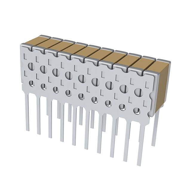
Surface Mount and Through-Hole Multilayer Ceramic Capacitors
KPS-MCL Low-Loss High Temperature 200°C SMPS Stacks,
200 – 2,000 VDC (Industrial Grade)
Overview
KEMET Power Solutions - Low loss (KPS MCL) High
Temperature SMPS Ceramic Stacked Capacitors combine
a robust and proprietary C0G/NPO base metal electrode
(BME) dielectric system with a durable lead-frame
technology for high temperature and high power SMPS
applications. These devices are specifically designed to
withstand the demands of harsh industrial environments
such as down-hole oil exploration and automotive/avionics
engine compartment circuitry.
The KPS-MCL is constructed with large chip multilayer
ceramic capacitors (MLCCs), vertically stacked and
secured to a lead-frame termination system, using a high
melting point (HMP) solder alloy. Vertically stacking the
capacitors in lead frames allows for much lower ESR (low
loss) and thermal resistance, which translates to very
high ripple current capability. The lead-frame isolates
the MLCCs from the printed circuit board (PCB), while
establishing a parallel circuit configuration.
Mechanically isolating the capacitors from the PCB improves
mechanical and thermal stress performance, while the
parallel circuit configuration allows for bulk capacitance in
the same or smaller design footprint.
KEMET’s high temperature C0G capacitors are temperaturecompensating and are well suited for resonant circuit
applications, or for those where Q and stability of
capacitance characteristics are required. They exhibit no
change in capacitance with respect to time and voltage, and
boast a negligible change in capacitance with reference to
ambient temperature. Capacitance change is limited to ±30
ppm/ºC from −55°C to +200°C. In addition, these capacitors
exhibit high insulation resistance with low dissipation factor
at elevated temperatures up to +200°C. They also exhibit
low ESR at high frequencies and offer greater volumetric
efficiency over competitive high temperature BME ceramic
capacitor devices.
Benefits
• Low-Loss
• Low ESR and ESL
• High thermal stability
• High ripple current capability
• Straight Pin lead wires for "through-hole" mounting
• Formed "J" and "L" lead wires for surface mounting
• Operating temperature range of −55°C to +200°C
• Case Codes (Case Sizes) – 69 (2220) and 70 (2225)
• DC voltage ratings of 200 – 2,000 V
• Capacitance offerings ranging from 11 nF – 1.2 µF
• Industrial grade
• High frequency performance and bulk capacitance in
a reduced footprint
Click image above for interactive 3D content
Open PDF in Adobe Reader for full functionality
One world. One KEMET
© KEMET Electronics Corporation • KEMET Tower • One East Broward Boulevard�
Fort Lauderdale, FL 33301 USA • 954-766-2800 • www.kemet.com
C1102_KPS-MCL_200C_STACKS • 3/31/2020
1
�Surface Mount and Through-Hole Multilayer Ceramic Capacitors
KPS-MCL Low-Loss High Temperature 200°C SMPS Stacks, 200 – 2,000 VDC (Industrial Grade)
Applications
• SMPS
• Input and output filtering on power supplies,
often found on “capacitor banks“
• Snubber circuits and DC link
• Resonator circuits
• Industrial
• Down-hole
• Defense and aerospace
• Hybrid and Electric Vehicles (HEVs, BEVs)
Ordering Information
L1
Product
Family
L1
G
N
69
Dielectric
Lead
Case Size/
Classification/
Configuration1 Case Code (CC)
Characteristic
G=
200°C C0G
(BME)
N = Straight
pin
L = Formed "L"
J = Formed "J"
69
70
C
224
K
A
03
Rated
Voltage
(DC)
Capacitance
Code (pF)
Capacitance
Tolerance
Lead/
Termination
Finish2
Number
of Chips
2 = 200 V
C = 500 V
B = 630 V
D = 1,000 V
F = 1,500 V
G = 2,000 V
Two
Significant
Digits and
number of
zeros
J = ±5%
K = ±10%
A = Silver
03 – 3 Chips
H = Solder
05 – 5 Chips
Coated (60/40) 10 – 10 Chips
Lead configuration and dimension details are outlined in the "Dimensions" section of this document. Additional lead configurations may be available.
Contact KEMET for details.
2
Solder coated (60/40) lead termination finish (H) only available for Straight pin (N) lead configuration.
1
Lead Configurations – Inches (Millimeters)
Lead Style
Symbol
Lead Style
L
Lead Length
N
(N) Straight
0.250 minimum
(6.35)
L
(L) Formed
0.055±0.005
(1.4±0.13)
J
(J) Formed
0.055±0.005
(1.4±0.13)
Additional lead configurations may be available. Contact KEMET for details.
© KEMET Electronics Corporation • KEMET Tower • One East Broward Boulevard�
Fort Lauderdale, FL 33301 USA • 954-766-2800 • www.kemet.com
C1102_KPS-MCL_200C_STACKS • 3/31/2020
2
�Surface Mount and Through-Hole Multilayer Ceramic Capacitors
KPS-MCL Low-Loss High Temperature 200°C SMPS Stacks, 200 – 2,000 VDC (Industrial Grade)
Dimensions – Inches (Millimeters)
Straight Lead (N)
Formed J Lead (J)
Formed L Lead (L)
E
E
C
Straight Lead (N)
Formed J (J) and L (L) Lead
G
D
D
A
B
A
B
L
L
C
E
J
F
L
C
J
H
G
H
B
K
F
K
LEAD ALIGNMENT
Note:
Lead alignment within pin rows
shall be 0.01” maximum.
Case
Code
C
Lead Spacing2
±0.025 (0.635)
69
0.25
(6.35)
70
1
2
E
Length
For
straight lead (N) and (J)
lead:
E = 0.30 (7.62) maximum
For
(L) lead:
E = 0.38 (9.65) maximum
Number Of
Leads Per
Side
D Width
±0.025
(0.635)
3
0.32
(8.13)
5
0.53
(13.5)
10
1.06
(26.9)
3
0.32
(8.13)
5
0.53
(13.5)
10
1.06
(26.9)
A
Height
Maximum
B
Height
Maximum
0.21
(5.33)
0.29
(7.37)
H
Lead
Pitch
0.1
(2.54)
0.26
(6.60)
0.34
(8.64)
K
Lead
Width
0.02
(0.5)
F
Seating Plane1
±0.010 (0.250)
For
straight lead (N),
seating plane
is 0.055"
For
(L) and (J) lead,
seating plane
is 0.070"
Mounting
Technique
Solder
reflow
only
Seating plane is the distance between the circuit board and the bottom of the lowest capacitor in the stack.
Lead spacing dimension from outside of lead frame.
© KEMET Electronics Corporation • KEMET Tower • One East Broward Boulevard�
Fort Lauderdale, FL 33301 USA • 954-766-2800 • www.kemet.com
C1102_KPS-MCL_200C_STACKS • 3/31/2020
3
�Surface Mount and Through-Hole Multilayer Ceramic Capacitors
KPS-MCL Low-Loss High Temperature 200°C SMPS Stacks, 200 – 2,000 VDC (Industrial Grade)
Environmental Compliance
KPS-MCL part types ≥ 500 V with silver (Ag) plating are RoHS compliant with exemption 7a.
Electrical Parameters/Performance Characteristics
Item
Parameters/Characteristics
Operating Temperature Range
Capacitance Change with Reference to +25°C
and 0 VDC Applied (TCC)
Aging Rate (Maximum % Capacitance Loss/Decade Hour)
Dielectric Withstanding Voltage (DWV)
1
Dissipation Factor (DF) Maximum Limit at 25°C 2
Insulation Resistance (IR) Minimum Limit at 25°C3
–55°C to +200°C
±30 ppm/°C (up to 200°C)
0%
250% of rated voltage for voltage rating of < 500 V
130% of rated voltage for voltage rating of ≥ 500 to < 1,000 V
120% of rated voltage for voltage rating of ≥ 1,000 V
(5 ±1 seconds and charge/discharge not exceeding 50 mA)
0.1%
1,000 MΩ µF or 100 GΩ
(Rated voltage applied for 120 ±5 seconds at 25°C)
DWV is the voltage a capacitor can withstand for a short period of time. It exceeds the nominal and continuous working voltage of a capacitor.
Capacitance and dissipation factor (DF) measured under the following conditions:
1 MHz ±100 kHz and 1.0 ±0.2 Vrms if capacitance ≤ 1,000 pF.
1 kHz ±50 Hz and 1.0 ±0.2 Vrms if capacitance > 1,000 pF.
3
To obtain IR limit, divide MΩ - µF value by the capacitance and compare to GΩ limit. Select the lower of the two limits.
Note: When measuring capacitance, it is important to ensure the set voltage level is held constant. The HP4284 and Agilent E4980 have a feature known
as Automatic Level Control (ALC). The ALC feature should be switched to "ON."
1
2
© KEMET Electronics Corporation • KEMET Tower • One East Broward Boulevard�
Fort Lauderdale, FL 33301 USA • 954-766-2800 • www.kemet.com
C1102_KPS-MCL_200C_STACKS • 3/31/2020
4
�Surface Mount and Through-Hole Multilayer Ceramic Capacitors
KPS-MCL Low-Loss High Temperature 200°C SMPS Stacks, 200 – 2,000 VDC (Industrial Grade)
Table 1 - Product Ordering Codes & Ratings
Height A
Inch (mm)
Maximum
D
Inch (mm)
Maximum
RoHS
Compliance
3
3
5
5
10
10
0.21 (5.3)
0.26 (6.6)
0.21 (5.3)
0.26 (6.6)
0.21 (5.3)
0.26 (6.6)
0.32 (8.13)
0.32 (8.13)
0.53 (13.5)
0.53 (13.5)
1.06 (26.92)
1.06 (26.92)
No
No
No
No
No
No
3
3
5
5
10
10
0.21 (5.3)
0.26 (6.6)
0.21 (5.3)
0.26 (6.6)
0.21 (5.3)
0.26 (6.6)
0.32 (8.13)
0.32 (8.13)
0.53 (13.5)
0.53 (13.5)
1.06 (26.9)
1.06 (26.9)
Yes
(see Note 4)
3
3
5
5
10
10
0.21 (5.3)
0.26 (6.6)
0.21 (5.3)
0.26 (6.6)
0.21 (5.3)
0.26 (6.6)
0.32 (8.13)
0.32 (8.13)
0.53 (13.5)
0.53 (13.5)
1.06 (26.9)
1.06 (26.9)
Yes
(see Note 4)
3
3
5
5
10
10
0.21 (5.3)
0.26 (6.6)
0.21 (5.3)
0.26 (6.6)
0.21 (5.3)
0.26 (6.6)
0.32 (8.13)
0.32 (8.13)
0.53 (13.5)
0.53 (13.5)
1.06 (26.9)
1.06 (26.9)
Yes
(see Note 4)
3
3
5
5
10
10
0.21 (5.3)
0.26 (6.6)
0.21 (5.3)
0.26 (6.6)
0.21 (5.3)
0.26 (6.6)
0.32 (8.13)
0.32 (8.13)
0.53 (13.5)
0.53 (13.5)
1.06 (26.9)
1.06 (26.9)
Yes
(see Note 4)
2220
2225
2220
2225
2220
2225
3
3
5
5
10
10
0.21 (5.3)
0.26 (6.6)
0.21 (5.3)
0.26 (6.6)
0.21 (5.3)
0.26 (6.6)
0.32 (8.13)
0.32 (8.13)
0.53 (13.5)
0.53 (13.5)
1.06 (26.9)
1.06 (26.9)
Yes
(see Note 4)
Chip Size
Number of Chips
Height A Inch (mm)
Maximum
D Inch (mm)
Maximum
RoHS Compliance
KEMET Part
Number1
Capacitance
(µF)2,3
Case
Code
Chip
Size
L1G(a)692284(b)(c)03
L1G(a)702364(b)(c)03
L1G(a)692464(b)(c)05
L1G(a)702604(b)(c)05
L1G(a)692924(b)(c)10
L1G(a)702125(b)(c)10
0.28
0.36
0.46
0.6
0.92
1.2
69
70
69
70
69
70
2220
2225
2220
2225
2220
2225
L1G(a)69C114(b)(c)03
L1G(a)70C144(b)(c)03
L1G(a)69C184(b)(c)05
L1G(a)70C234(b)(c)05
L1G(a)69C364(b)(c)10
L1G(a)70C474(b)(c)10
0.11
0.14
0.18
0.23
0.36
0.47
69
70
69
70
69
70
2220
2225
2220
2225
2220
2225
L1G(a)69B663(b)(c)03
L1G(a)70B843(b)(c)03
L1G(a)69B114(b)(c)05
L1G(a)70B144(b)(c)05
L1G(a)69B224(b)(c)10
L1G(a)70B284(b)(c)10
0.066
0.084
0.11
0.14
0.22
0.28
69
70
69
70
69
70
2220
2225
2220
2225
2220
2225
L1G(a)69D393(b)(c)03
L1G(a)70D543(b)(c)03
L1G(a)69D653(b)(c)05
L1G(a)70D903(b)(c)05
L1G(a)69D134(b)(c)10
L1G(a)70D184(b)(c)10
0.039
0.054
0.065
0.090
0.130
0.180
69
70
69
70
69
70
2220
2225
2220
2225
2220
2225
L1G(a)69F163(b)(c)03
L1G(a)70F203(b)(c)03
L1G(a)69F273(b)(c)05
L1G(a)70F343(b)(c)05
L1G(a)69F533(b)(c)10
L1G(a)70F683(b)(c)10
0.016
0.020
0.027
0.034
0.053
0.068
69
70
69
70
69
70
2220
2225
2220
2225
2220
2225
L1G(a)69G113(b)(c)03
L1G(a)70G143(b)(c)03
L1G(a)69G183(b)(c)05
L1G(a)70G233(b)(c)05
L1G(a)69G363(b)(c)10
L1G(a)70G473(b)(c)10
0.011
0.014
0.018
0.023
0.036
0.047
69
70
69
70
69
70
KEMET Part Number1
Capacitance (µF)2,3
Case Code
Number
of Chips
200 V
500 V
630 V
1,000 V
1,500 V
2,000 V
Complete part number requires additional characters in the numbered positions provided in order to indicate lead configuration, capacitance tolerance
and lead finish. For each numbered position, available options are as follows:
(a) Lead style character "N," "L," or "J."
(b) Capacitance tolerance character "J" or "K."
(c) Lead finish character "A" for 100% Ag, "H" for solder coated.
2
Capacitance values listed are for stacked components and do not follow E12, E24 format defined by BS 2488 standard. Please contact factory to
inquire about capacitance values not listed.
3
Identical capacitance values may be listed for the same voltage rating. User can select which case size and chip count is desired for the given
capacitance value.
4
KPS-MCL Stacked Capacitors ≥ 500 V with Ag plating are RoHS compliant by exemption 7a.
1
© KEMET Electronics Corporation • KEMET Tower • One East Broward Boulevard�
Fort Lauderdale, FL 33301 USA • 954-766-2800 • www.kemet.com
C1102_KPS-MCL_200C_STACKS • 3/31/2020
5
�Surface Mount and Through-Hole Multilayer Ceramic Capacitors
KPS-MCL Low-Loss High Temperature 200°C SMPS Stacks, 200 – 2,000 VDC (Industrial Grade)
Soldering Process
The capacitors and assemblies outlined in this specification sheet are susceptible to thermal shock damage due to their
large ceramic mass. Temperature profiles used should provide adequate temperature rise and cool-down time to prevent
damage from thermal shock. In general, KEMET recommends against hand-soldering for these types of large ceramic
devices, but if hand-soldering cannot be avoided, refer to hand-soldering section below.
Recommended Soldering Technique:
• Solder reflow
Recommended Reflow Soldering Profile:
TP
Temperature
TL
tP
Maximum Ramp Up Rate = 2°C/second
Maximum Ramp Down Rate = 2°C/second
tL
Tsmax
Tsmin
25
ts
25°C to Peak
Time
Profile Feature
Sn-Pb
Pb-Free
Temperature Minimum (TSmin)
Temperature Maximum (TSmax)
Time (ts) from Tsmin to Tsmax)
Ramp-up rate (TL to TP)
Liquidous temperature (TL)
Time above liquidous (tL)
Peak temperature (TP)
100°C
150°C
60 – 90 seconds
2°C/second
183°C
95 seconds
240°C
150°C
200°C
60 – 120 seconds
3°C/second
217°C
95 seconds
260°C
Time within 5°C of maximum peak
temperature (tP)
5 seconds
5 seconds
Ramp-down rate (TP to TL)
Time 25°C to peak temperature
2°C/second
3.5 minutes
2°C/second
3.5 minutes
Preheat/Soak
Note: All temperatures refer to the center of the package, measured on the package body surface that is facing up during assembly reflow.
Preheating and Reflow Profile Notes:
Due to the differences in the coefficient of the thermal expansion for the different materials of construction, it is critical to monitor and control the heating
and cooling rates during the soldering process. To ensure optimal component reliability, KEMET's recommended heating and cooling rate is 2°C/second.
After soldering, the capacitors should be air cooled to room temperature before further processing. Forced air cooling is not recommended.
© KEMET Electronics Corporation • KEMET Tower • One East Broward Boulevard�
Fort Lauderdale, FL 33301 USA • 954-766-2800 • www.kemet.com
C1102_KPS-MCL_200C_STACKS • 3/31/2020
6
�Surface Mount and Through-Hole Multilayer Ceramic Capacitors
KPS-MCL Low-Loss High Temperature 200°C SMPS Stacks, 200 – 2,000 VDC (Industrial Grade)
Soldering Process cont.
Recommendations for Hand-Soldering:
Care should be taken when hand-soldering large ceramic stacks. Excessive thermal shock on the ceramic material can lead
to cracking and reliability issues. To reduce risk of thermal shock, KEMET recommends solder reflow, but if hand soldering
cannot be avoided, please see recommended guidelines below.
Pre-Heating
Stacks should be preheated to a temperature within 50°C of reflow temperature. KEMET recommends a ramp rate of 2°C/
second to avoid thermal shock during the pre-heating process.
Hand-Soldering
When using a solder iron, keep tip of the iron as far away from ceramic body to avoid excessive heating.
Cool Down
After reflow, stacks should be allowed to cool at a preferable rate of 2°C/second until room temperature is reached.
Storage & Handling
Ceramic capacitors should be stored in normal working environments. While the chips themselves are quite robust in
other environments, solderability will be degraded by exposure to high temperatures, high humidity, corrosive atmospheres,
and long term storage. In addition, packaging materials will be degraded by high temperature–reels and may soften or warp,
and tape peel force may increase. KEMET recommends that maximum storage temperature does not exceed 40°C and
maximum storage humidity does not exceed 70% relative humidity. Temperature fluctuations should be minimized to
avoid condensation on the parts. Atmospheres should be free of chlorine and sulfur bearing compounds. For optimized
solderability chip stock should be used promptly, preferably within 1.5 years of receipt.
© KEMET Electronics Corporation • KEMET Tower • One East Broward Boulevard�
Fort Lauderdale, FL 33301 USA • 954-766-2800 • www.kemet.com
C1102_KPS-MCL_200C_STACKS • 3/31/2020
7
�Surface Mount and Through-Hole Multilayer Ceramic Capacitors
KPS-MCL Low-Loss High Temperature 200°C SMPS Stacks, 200 – 2,000 VDC (Industrial Grade)
Table 2 - Performance & Reliability: Test Methods & Conditions
Inspection
Test Method
Test Conditions
Reliability/Environmental Tests
High Temperature Life
MIL–STD–202, Method 108
200°C, rated voltage, 1,000 hours
JESD22, Method JA–104
–55°C to +200°C, 300 cycles
Thermal Shock
MIL–STD–202, Method 107
–55°C to +200°C, 20 seconds transfer,
15 minutes dwell, 20 cycles
Moisture Resistance
MIL–STD–202, Method 106
20 cycles, no voltage applied
Temperature Cycling
Physical, Mechanical and Process Tests
Vibration
MIL–STD–202, Method 204
Condition D per MIL–PRF–49470, simple
harmonic, 20 g peak, 10 – 2,000 Hz,
20 minute sweep, 12 sweeps per axis
Resistance to Soldering Heat
MIL–STD–202, Method 210
Condition B, 260°C, 10 seconds
Terminal Strength
MIL–STD–202, Method 202
Condition A
Immersion
MIL–STD–202, Method 104
Condition B
J–STD–002C
Category 3
For Sn-Pb solder alloy:
Method A, 245°C, 5 seconds
Method S, 220°C peak
For Pb-Free solder alloy:
Method A1, 260°C, 5 seconds
Method S1, 245°C peak
Solderability
© KEMET Electronics Corporation • KEMET Tower • One East Broward Boulevard�
Fort Lauderdale, FL 33301 USA • 954-766-2800 • www.kemet.com
C1102_KPS-MCL_200C_STACKS • 3/31/2020
8
�Surface Mount and Through-Hole Multilayer Ceramic Capacitors
KPS-MCL Low-Loss High Temperature 200°C SMPS Stacks, 200 – 2,000 VDC (Industrial Grade)
Construction
Detailed Cross Section
Dielectric material
(CaZrO3)
Lead-frame
(Phosphor Bronze -Alloy 510)
Inner electrodes
(Ni)
Dielectric material
(CaZrO3)
Lead-frame
attach solder
End termination/
External electrode
(Cu)
Barrier layer
(Ni)
Termination finish
(Sn10/Pb88/Ag2)
Barrier layer
(Ni)
Inner electrodes
(Ni)
Lead-frame finish
(Ag or Sn60/Pb40)
End termination/
External electrode
(Cu)
Termination finish
(Sn10/Pb88/Ag2)
Packaging
Waffle Packaging Quantities
1
Case Code
Lead Style
69
L/J/N
70
L/J/N
Number of Chips in
Stack
Waffle Pack
Quantity1
3 and 5
10
3 and 5
10
50
25
50
25
Minimum order value applies. Contact KEMET for details.
© KEMET Electronics Corporation • KEMET Tower • One East Broward Boulevard�
Fort Lauderdale, FL 33301 USA • 954-766-2800 • www.kemet.com
C1102_KPS-MCL_200C_STACKS • 3/31/2020
9
�Surface Mount and Through-Hole Multilayer Ceramic Capacitors
KPS-MCL Low-Loss High Temperature 200°C SMPS Stacks, 200 – 2,000 VDC (Industrial Grade)
KEMET Electronics Corporation Sales Offices
For a complete list of our global sales offices, please visit www.kemet.com/sales.
Disclaimer
All product specifications, statements, information and data (collectively, the “Information”) in this datasheet are subject to change. The customer is responsible for
checking and verifying the extent to which the Information contained in this publication is applicable to an order at the time the order is placed. All Information given
herein is believed to be accurate and reliable, but it is presented without guarantee, warranty, or responsibility of any kind, expressed or implied.
Statements of suitability for certain applications are based on KEMET Electronics Corporation’s (“KEMET”) knowledge of typical operating conditions for such
applications, but are not intended to constitute – and KEMET specifically disclaims – any warranty concerning suitability for a specific customer application or use.
The Information is intended for use only by customers who have the requisite experience and capability to determine the correct products for their application. Any
technical advice inferred from this Information or otherwise provided by KEMET with reference to the use of KEMET’s products is given gratis, and KEMET assumes
no obligation or liability for the advice given or results obtained.
Although KEMET designs and manufactures its products to the most stringent quality and safety standards, given the current state of the art, isolated component
failures may still occur. Accordingly, customer applications which require a high degree of reliability or safety should employ suitable designs or other safeguards
(such as installation of protective circuitry or redundancies) in order to ensure that the failure of an electrical component does not result in a risk of personal injury
or property damage.
Although all product–related warnings, cautions and notes must be observed, the customer should not assume that all safety measures are indicted or that other
measures may not be required.
KEMET is a registered trademark of KEMET Electronics Corporation.
© KEMET Electronics Corporation • KEMET Tower • One East Broward Boulevard�
Fort Lauderdale, FL 33301 USA • 954-766-2800 • www.kemet.com
C1102_KPS-MCL_200C_STACKS • 3/31/2020
10
�


 工商网监
湘ICP备2023018690号
工商网监
湘ICP备2023018690号
