MOSFET
SMD Type
Complementary Trench MOSFET
AO6601
(KO6601)
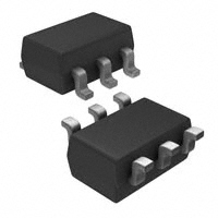
8QLW� PP
( SOT-23-6 )
+0.1
0.4 -0.1
6
5
4
1
2
3
����
1.6 ����
ƽ VDS (V) = 30V
����
2.8 ����
N-Channel :
���
Ƶ Features
ƽ RDS(ON) ˘ 60m¡ (VGS = 10V)
����
ƽ ID = 3.4 A (VGS = 10V)
ƽ RDS(ON) ˘ 70m¡ (VGS = 4.5V)
�����
���� �����
+0.01
-0.01
ƽ RDS(ON) ˘ 90m¡ (VGS = 2.5V)
+0.2
-0.1
����
��� ����
P-Channel :
ƽ VDS (V) = -30V
ƽ ID = -2.3 A (VGS = 10V)
�����
ƽ RDS(ON) ˘ 150m¡ (VGS = -4.5V)
1 G1
2 S2
3 G2
����
���� ����
ƽ RDS(ON) ˘ 115m¡ (VGS = -10V)
4 D2
5 S1
6 D1
ƽ RDS(ON) ˘ 200m¡ (VGS = -2.5V)
D1
G1
D2
G2
S1
N-channel
S2
P-channel
Ƶ Absolute Maximum Ratings Ta = 25ć
Parameter
Symbol
N-Channel
P-Channel
Drain-Source Voltage
VDS
30
-30
Gate-Source Voltage
VGS
Continuous Drain Current
TA=25ć
ID
TA=70ć
Pulsed Drain Current
Power Dissipation
IDM
TA=25ć
PD
TA=70ć
Thermal Resistance.Junction- to-Ambient
t İ 10s
RthJA
Steady-State
Thermal Resistance.Junction- to-Lead
Junction Temperature
Storage Temperature Range
f12
3.4
-2.3
2.7
-1.8
20
Unit
V
A
-15
1.15
W
0.73
110
ć/W
150
RthJL
80
TJ
150
Tstg
-55 to 150
ć
www.kexin.com.cn
1
�MOSFET
SMD Type
Complementary Trench MOSFET
AO6601
(KO6601)
Ƶ N-Channel Mosfet Electrical Characteristics Ta = 25ć
Parameter
Symbol
Drain-Source Breakdown Voltage
VDSS
Zero Gate Voltage Drain Current
IDSS
Gate-Body Leakage Current
Gate Threshold Voltage
Test Conditions
Min
Typ
30
ID=250A, VGS=0V
VDS=30V, VGS=0V
1
VDS=30V, VGS=0V, TJ=55ć
5
IGSS
VDS=0V, VGS=f12V
VGS(th)
VDS=VGS , ID=250uA
RDS(On)
0.5
VDS=5V, ID=3.4A
Input Capacitance
Ciss
Coss
Crss
Gate Resistance
Rg
Total Gate Charge (10V)
60
88
TJ=125ć
m¡
20
A
14
�
VGS=0V, VDS=15V, f=1MHz
VGS=0V, VDS=0V, f=1MHz
Qg
Total Gate Charge (4.5V)
V
90
VGS=10V, VDS=5V
Output Capacitance
1.5
VGS=2.5V, ID=2A
gFS
Reverse Transfer Capacitance
nA
70
ID(ON)
uA
f100
VGS=4.5V, ID=3A
Forward Transconductance
On State Drain Current
VGS=10V, VDS=15V, ID=3.4A
S
182
285
25
45
10
25
0.9
2.7
10
12
4.7
6
pF
¡
nC
Qgs
0.95
Gate Drain Charge
Qgd
1.6
Turn-On DelayTime
td(on)
3.5
Turn-On Rise Time
tr
Turn-Off DelayTime
td(off)
17.5
Turn-Off Fall Time
tf
2.5
Body Diode Reverse Recovery Time
trr
Body Diode Reverse Recovery Charge
Qrr
4
nC
Maximum Body-Diode Continuous Current
IS
1.5
A
1
V
Gate Source Charge
Diode Forward Voltage
2
VGS=10V, ID=3.4A
Unit
V
VGS=10V, ID=3.4A
Static Drain-Source On-Resistance
Max
www.kexin.com.cn
VSD
VGS=10V, VDS=15V, RL=4.4¡,RG=3¡
IF= 3.4A, dI/dt= 100A/s
IS=1A,VGS=0V
1.5
ns
12
�MOSFET
SMD Type
Complementary Trench MOSFET
AO6601
(KO6601)
Ƶ P-Channel Mosfet Electrical Characteristics Ta = 25ć
Parameter
Drain-Source Breakdown Voltage
Zero Gate Voltage Drain Current
Gate-Body leakage current
Gate Threshold Voltage
Symbol
VDSS
IDSS
IGSS
VGS(th)
Test Conditions
Min
Typ
-30
ID=-250A, VGS=0V
-1
VDS=-30V, VGS=0V, TJ=55ć
-5
VDS=0V, VGS=f12V
-0.6
VDS=VGS , ID=-250A
On state drain current
RDS(On)
ID(ON)
Forward Transconductance
gFS
Input Capacitance
Ciss
Output Capacitance
Coss
Reverse Transfer Capacitance
Crss
Gate resistance
Rg
Total Gate Charge (10V)
VGS=-10V, ID=-2.3A
VGS=-2.5V, ID=-1A
200
VGS=-10V, VDS=-5V
-15
VDS=-5V, ID=-2.3A
VGS=0V, VDS=-15V, f=1MHz
VGS=0V, VDS=0V, f=1MHz
315
25
50
10
30
4
12
4.5
7
2
4
Qgd
1
Turn-On DelayTime
td(on)
6
Turn-On Rise Time
tr
Turn-Off DelayTime
td(off)
20
tf
5
trr
Maximum Body-Diode Continuous Current
IS
Diode Forward Voltage
VSD
IF=-2.3A, dI/dt=100A/s
IS=-1A,VGS=0V
S
205
Gate Drain Charge
VGS=-10V, VDS=-15V, RL=6¡,RG=3¡
m¡
A
8
0.7
Qrr
V
150
Qgs
Body Diode Reverse Recovery Time
nA
-1.4
200
TJ=125ć
VGS=-10V, VDS=-15V, ID=-2.3A
Body Diode Reverse Recovery Charge
f100
VGS=-4.5V, ID=-2A
Gate Source Charge
Turn-Off Fall Time
uA
115
Qg
Total Gate Charge (4.5V)
Unit
V
VDS=-30V, VGS=0V
VGS=-10V, ID=-2.3A
Static Drain-Source On-Resistance
Max
pF
¡
nC
3.5
ns
15
6
nC
-1.5
A
-1
V
Ƶ Marking
Marking
F1
www.kexin.com.cn
3
�MOSFET
SMD Type
Complementary Trench MOSFET
AO6601
(KO6601)
Ƶ N-Channel Mosfet Typical Characterisitics
15
15
10V
VDS=5V
2.5V
3V
12
12
4.5V
9
ID(A)
ID (A)
9
6
6
VGS=2V
125eC
3
3
0
0
0
1
2
3
4
0
5
VDS (Volts)
Fig 1: On-Region Characteristics
0.5
1
1.5
2
2.5
3
VGS(Volts)
Figure 2: Transfer
� Characteristics
80
Normalized On-Resistance
2
VGS=2.5V
70
:)
RDS(ON) (m:
25eC
60
VGS=4.5V
50
40
VGS=10V
30
1.8
VGS=4.5V
ID=3A
1.6
1.4
VGS=2.5V
5
ID=2A
2
1.2
VGS=10V
ID=3.4A
1
0.8
0
2
4
6
8
10
.
ID (A)
Figure 3: On-Resistance vs. Drain Current and Gate
Voltage
0
140
25
50
75
100
125
150
175
Temperature (°C)
Figure 4: On-Resistance vs. Junction Temperature
1.0E+02
ID=3.4A
1.0E+01
120
1.0E+00
125eC
IS (A)
:)
RDS(ON) (m:
100
80
125eC
1.0E-02
60
25eC
25eC
1.0E-03
40
1.0E-04
20
1.0E-05
0
4
6
8
10
VGS (Volts)
Figure 5: On-Resistance vs. Gate-Source Voltage
4
1.0E-01
2
www.kexin.com.cn
0.0
0.2
0.4
0.6
0.8
1.0
VSD (Volts)
Figure 6: Body-Diode Characteristics
1.2
�MOSFET
SMD Type
Complementary Trench MOSFET
AO6601
(KO6601)
Ƶ N-Channel Mosfet Typical Characterisitics
10
500
VDS=15V
ID=3.4A
400
Capacitance (pF)
VGS (Volts)
8
6
4
Ciss
300
200
Coss
2
100
0
0
Crss
0
3
6
9
Qg (nC)
Figure 7: Gate-Charge Characteristics
0
12
100.0
5
10
15
20
25
VDS (Volts)
Figure 8: Capacitance Characteristics
30
1000
TA=25eC
RDS(ON)
limited
10Ps
100Ps
1.0
10ms
1ms
TJ(Max)=150eC
TA=25eC
0.1
DC
100
Power (W)
ID (Amps)
10.0
10
10s
1
0.0
0.01
0.1
1
VDS (Volts)
10
Figure 9: Maximum Forward Biased
Safe Operating Area (Note F)
100
0.00001
0.001
0.1
10
1000
Pulse Width (s)
Figure 10: Single Pulse Power Rating Junctiont A bi t (Note
to-Ambient
(N t F)
ZT JA Normalized Transient
Thermal Resistance
10
In descending order
D=0.5, 0.3, 0.1, 0.05, 0.02, 0.01, single pulse
D=Ton/T
TJ,PK=TA+PDM.ZTJA.RTJA
1
RTJA=150eC/W
0.1
Single Pulse
0.01
PD
Ton
T
0.001
0.00001
0.0001
0.001
0.01
0.1
1
10
Pulse Width (s)
Figure 11: Normalized Maximum Transient Thermal Impedance (Note F)
100
1000
www.kexin.com.cn
5
�MOSFET
SMD Type
Complementary Trench MOSFET
AO6601
(KO6601)
Ƶ P-Channel Mosfet Typical Characterisitics
10
15
-10V
VDS=-5V
-4.5V
-3V
12
8
6
-2.5V
-ID(A)
-ID (A)
9
4
6
125eC
25eC
VGS=-2V
3
2
0
0
0
1
2
3
4
0
5
-VDS (Volts)
Fig 1: On-Region Characteristics
0.5
1
1.5
2
2.5
3
3.5
4
-VGS(Volts)
Figure 2: Transfer Characteristics
�
210
2
Normalized On-Resistance
VGS=-2.5V
190
RDS(ON) (m:
:)
170
150
VGS=-4.5V
130
110
90
VGS=-10V
70
50
VGS=-10V
ID=-2.3A
1.8
1.6
1.4
VGS=-4.5V
ID=-2A 2
1.2
VGS=-2.5V
ID=-1A
1
0.8
0
2
4
6
8
-ID (A)
Figure 3: On-Resistance vs. Drain Current and Gate
Voltage
0
25
50
75
100
125
150
175
Temperature (°C)
Figure 4: On-Resistance vs. Junction Temperature
1.0E+02
250
ID=-2.3A
1.0E+01
1.0E+00
125eC
125eC
-IS (A)
RDS(ON) (m:
:)
200
150
1.0E-01
25eC
1.0E-02
25eC
1.0E-03
100
1.0E-04
50
1.0E-05
0
4
6
8
10
-VGS (Volts)
Figure 5: On-Resistance vs. Gate-Source Voltage
6
2
www.kexin.com.cn
0.0
0.2
0.4
0.6
0.8
1.0
-VSD (Volts)
Figure 6: Body-Diode Characteristics
1.2
�MOSFET
SMD Type
Complementary Trench MOSFET
AO6601
(KO6601)
Ƶ P-Channel Mosfet Typical Characterisitics
500
10
VDS=-15V
ID=-2.3A
400
Capacitance (pF)
-VGS (Volts)
8
6
4
Ciss
300
200
Coss
2
100
0
0
0
1
2
3
4
5
Qg (nC)
Figure 7: Gate-Charge Characteristics
Crss
0
6
5
10
15
20
25
-VDS (Volts)
Figure 8: Capacitance Characteristics
30
1000
100.0
TA=25eC
10Ps
100Ps
1.0
1ms
10ms
0.1
100
Power (W)
RDS(ON)
limited
10
DC
TJ(Max)=150eC
TA=25eC
10s
0.0
1
0.01
0.1
1
-VDS (Volts)
10
100
0.00001
Figure 9: Maximum Forward Biased Safe
Operating Area
0.001
0.1
10
1000
Pulse Width (s)
Figure 10: Single Pulse Power Rating Junctionto-Ambient
10
ZT JA Normalized Transient
Thermal Resistance
-ID (Amps)
10.0
D=Ton/T
TJ,PK=TA+PDM.ZTJA.RTJA
1
In descending order
D=0.5, 0.3, 0.1, 0.05, 0.02, 0.01, single pulse
RTJA=150eC/W
0.1
0.01
PD
Single Pulse
Ton
T
0.001
0.00001
0.0001
0.001
0.01
0.1
1
10
100
1000
Pulse Width (s)
Figure 11: Normalized Maximum Transient Thermal Impedance
www.kexin.com.cn
7
�