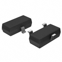
SMD Type
N-Channel PowerTrench MOSFET FDN5630
MOSFET
■ Features
● VDS (V) = 60V ● RDS(ON)<100 mΩ (VGS = 10V)
2.4-+00..11
SOT-23
+0.1 2.9-0.1 +0.1 0.4-0.1
Unit: mm
1
2
+0.1 0.95-0.1 +0.1 1.9-0.1
● Low gate charge ● Very fast switching
0.55
● Optimized for use in high frequency DC/DC converters
1.3-+00..11
● RDS(ON)<120 mΩ (VGS = 6V)
0.4
3
+0.05 0.1-0.01
0.97-+00..11
1.Base 1. Gate
0.38-+00..11
0-0.1
2.Emitter 2. Source
3. Drain 3.collector
■ Absolute Maximum Ratings Ta = 25℃
Parameter Drain-Source Voltage Gate-to-source voltage Drain curent -Continuous -Pulsed Power dissipation Maximum Junction-to-Ambient Junction and storage temperature range PD RθJA TJ,TSTG Symbol VDS VGS ID Rating 60 ±20 1.7 10 0.5 250 -55 to +150 W ℃/ W ℃ Unit V V A
www.kexin.com.cn
1
�SMD Type
N-Channel PowerTrench MOSFET FDN5630
■ Electrical Characteristics Ta = 25℃
Parameter Drain-source Breakdown voltage Breakdown Voltage Temperature Coefficient Symbol V(BR)DSS
△V(BR)DSS/△TJ
MOSFET
Testconditons ID= 250 μA, VGS = 0V ID = 250μA, Referenced to 25℃ ID= 1.7A, VGS = 10V
Min 60
Typ
Max
Unit V
63 73 127 83 1 2.4 6 1 -100 100 7 10 100 180 120 3
mV/℃
Static drain-source on- resistance
RDS(on)
ID= 1.7A, VGS = 10V Ta = 125℃ ID= 1.6A, VGS = 6V
mΩ
Gate threshold voltage Forward Transconductance Gate-source leakage current Gate-source forward leadage Gate-source reverse leadage Total Gate Charge Gate-Source Charge Gate-Drain Charge Turn-on delay time Rise time Turn-off delay time Fall time Input capacitance Output capacitance Reverse transfer capacitance Maximum Continuous Drain-Source Diode Forward Current Diode forward voltage
VGS(th) gfs IDSS IGSS Qg Qgs Qgd td(on) tr td(off) tr Ciss Coss Crss IS VSD
VDS = VGS, ID= 250 μA VDS = 10 V, ID = 1.7 A VDS = 48 V, VGS = 0V VGS =-20V VGS =20V VDS =20V ,VGS = 10 V , ID=1.7 A
V S μA nA
1.6 1.2 10 20 15 28 15
nC
VDD= 30 V, ID= 1 A VGS =10 V, RGEN= 6 Ω
6 15 5
ns
VDS = 15 V, VGS = 0 V, f= 1MHz
400 102 21 0.42 A V pF
VGS = 0 V , IS = 0.42 A
0.72
1.2
www.kexin.com.cn
2
�
很抱歉,暂时无法提供与“FDN5630”相匹配的价格&库存,您可以联系我们找货
免费人工找货