High-Q MLC Capacitors
Low ESR MLC Capacitors
Single Layer Capacitors
Broadband Blocking Capacitors
Thin Film Ceramic Filters
High-K Ceramic Substrates and Plates
Thin Film Resonators
Thin Film Gain Equalizers
Custom Ceramic Components
MLC & SLC Capacitors
Thin Film Components
www.dilabs.com
�Introduction to Dielectric Laboratories Inc.
What makes DLI Unique?
DLI built its global reputation as a manufacturer of high frequency,
High Q capacitors. In recent years, DLI has emerged as a
comprehensive manufacturer of specialty ceramic components for
application specific microwave and millimeter wave components
serving customers in fiber optic, wireless, medical, transportation,
semiconductor, space, avionics and military markets.
DLI continues to introduce exciting new innovations in custom
ceramic resonator and filter technologies. These patent-protected
products leverage decades of ceramic and Thin Film experience,
creative and clever design expertise, and advanced prototyping
and testing capabilities. Please discuss your needs with our Sales
and Applications Engineering Team.
With over four decades of material science formulation and
development, more than one hundred proprietary and/or patented
ceramic formulations, and multiple recent patent filings, DLI is the
pre-eminent ceramic component manufacturer in the industry. The
marriage of ceramic expertise, manufacturing know-how, product
quality, customer service, product customization, and clever
microwave and RF design engineering sets us apart from all others
in the industry.
Heat Sinks and Resonator Components complete our portfolio.
DLI offers a broad range of Multi-Layer Capacitor products.
We have the most comprehensive array of Broadband Blocking
capacitors. We have expertise in customizing, tight tolerances and
meeting specific design targets.
DLI is the preeminent global supplier of Single-Layer Capacitors.
We have the world’s broadest range of materials starting with
Class 1 dielectrics with ξr from 5.7 to 900 and Class 2 dielectrics
with ξr from 445 to 25,000. DLI specializes in high reliability and
space applications.
Our Build-to-Print services designed to facilitate thin film product
design, manufacturing and testing from prototype to high volume
production. Our custom ceramics offer significantly better thermal
performance than majority of industry standard ceramics and
have an added benefit of a sufficiently higher dielectric constant
(K) allowing miniaturization opportunities and temperature stable
performance.
RoHS Compliance Statement
DLI is a leading supplier to the electronic components market
and is fully committed to offering products supporting Restriction
of Hazardous Substances (RoHS) directive 2011/65/Eu. All of
our Dielectric formulations are RoHS compliant and we offer a
broad range of capacitors with RoHS compliant terminations. DLI
complies with the requirements of the individual customer and will
maintain product offerings that meet the demands of our industry.
Quality and Environmental Policy
DLI’s reputation for quality and environmental responsibility
is based on a commitment not only to meet our customers’
requirements, but to exceed their expectations. The entire
organization, beginning with top management, strives to achieve
excellence in designing, manufacturing and delivering High Q
capacitors and proprietary thin film components for niche high
frequency applications, while maintaining safe and healthy working
conditions. Furthermore, DLI commits to achieve these goals in
an environmentally responsible manner through our commitment
to comply with environmental regulations and implement pollution
prevention initiatives. DLI strives to continually improve the
effectiveness of our Quality and Environmental Management
System through the establishment and monitoring of objectives
and targets.
ISO 14001
Environmental
www.dilabs.com
�Contents
Introduction
About Us.............................................................................................. Inside front cover
What’s New at DLI............................................................................................................2
Simplified Frequency & Application Chart............................................................................3
Single Layer Capacitors
General Information...................................................................................................... 4-6
Packaging.........................................................................................................................7
Border Cap® 1 or 2-sided recessed metallization............................................................ 8-11
T-Cap® Transmission Line Capacitor..................................................................................12
Di-Cap® 1MHz to > 80GHz......................................................................................... 13-15
Bar Cap® Multiple arrays..................................................................................................16
Gap Cap® to eliminate wire bonding........................................................................... 17-19
Bi-Cap® Binary Capacitor.................................................................................................20
Heatsinks, Standoffs & Submounts...................................................................................21
Multilayer Ceramic Capacitors
Material & Case Size Summary Sheets........................................................................ 22-23
Application Notes...................................................................................................... 24-25
General Information.................................................................................................. 26-27
Standard Part Number System.........................................................................................28
AH Series: P90 Porcelain Capacitors............................................................................ 29-31
CF Series: Ultrastable Porcelain Capacitors.................................................................. 32-34
NA Series: N30 Porcelain Capacitors.................................................................................35
UL Series: Ultra Low ESR Ceramic Capacitors.............................................................. 36-38
High Q Capacitors - C04, C06, C11 & C17 Kits...................................................................39
Broadband Blocking Capacitors
C04/C06/C08 Broadband Blocking Capacitor......................................................................40
Opti-Cap® Ultra Broadband DC Blocking...................................................................... 41-43
Milli-Cap® Millimeter Wave Broadband Blocking Capacitor...................................................44
Miniature RF Blocking Network................................................................................... 45-46
Thin Film Devices
RF Guru Ceramic Filter Request Form...............................................................................47
Ceramic Filters product summary............................................................................... 48-49
Filter Packaging, Shielding and Mounting.................................................................... 50-51
Filter Temperature Stability..............................................................................................52
Surface Mount Lowpass Filter Series.................................................................................53
2-18 GHz Bandpass Filter Series.......................................................................................54
Wilkinson Power Divider...................................................................................................55
Symmetric Dual Mode Resonator Filter..............................................................................56
10GHz 4 Pole Band Pass with Bandstop Filter....................................................................56
20GHz 8 Pole SMT Filter..................................................................................................56
36GHz Filter Repeatability................................................................................................56
GPS Filters......................................................................................................................57
High-K Ceramic Substrate and Plates................................................................................58
Ceramic Cavity Resonators......................................................................................... 59-65
Self Bias Network...................................................................................................... 63-64
Gain Equalizers......................................................................................................... 65-67
Build to Print...................................................................................................................68
www.dilabs.com | Phone: +1.315.655.8710 |
1
�What’s New at DLI
0402
S
Catalog Filters
0402 product line extension
of Z type plating (Sn over
Ni) in the C04 (0402) case
size with its Ultra-Low
ESR UL dielectric material.
Previously the C04 product
line was only available in
“S” type plating (Au flash
over Ni).
Z
Plating Code
Layers
Applications
“S”
• Au Flash (3-5µ”)
• Ni barrier Layer
• Ag Termination
• Specialty Solder & Epoxy
“Z”
• Sn plated solder
• Ni barrier layer
• Ag Termination
• High Volume & Hand Solder
Both termination types are fully RoHS compliant
Dielectric Laboratories Inc. C04 case size meets the EIA
0402 footprint, which is perfectly suited for High Frequency
decoupling type of applications.
Milli-Caps®
Available in 0402, 0502
and 0602 footprints
with capacitance values
ranging from 0.3pF to
82pF. These capacitors
are perfect for testing
equipment, photonics,
SONET, digital radios
and matching filter
applications. A usable frequency range up to 40GHz with
very low series inductance and ultra-high series resonance
makes this the ideal capacitor for your broadband blocking
needs.
50V UX material
The UX material space
qualified to MILPRF-38534 Class K is
now available in a 50V
rating. DLI’s broad
range of standard
architectures, including
Di-Caps®, Border Caps®,
Bar Caps® and Gap
Caps® can utilize the
new 50V rated high
K dielectric. UX has
the highest dielectric constant of any of DLI’s wide variety
of materials. The high dielectric constant (K) allows for
higher capacitance values in smaller case sizes. This means
smaller components on your boards without sacrificing
performance!
2
• Ultra-High Dielectric Constant K=25,000
• X7R Temperature Stability
• Highest Capacity Density SLC
• Ideal for Epoxy & Wire Bond Assembly
• Voltage Rating of 25V & 50V
• Rugged Ceramic & Thin Film Gold
• Excellent Dimensional Tolerance
| Phone: +1.315.655.8710 | www.dilabs.com
Newly released Catalog
Lowpass and Bandpass
Filters for high
frequency applications.
This small, surface
mount filters have
temperature stable
performance from 2
GHz up to 50 GHz. The
filters integrate DLI’s
high dielectric, temperature stable ceramic materials to offer
high reliability in environmentally challenging conditions.
Continue to check our website for new additions.
Cavity Filters
Ceramic cavity resonator
technology can be
employed in conjunction
with DLI’s stable, high
Q ceramics to create
highly selective, small,
low loss band pass
filters. Using a multiport implementation, a
very small robust filter
can be created. Wide reject band performance without
spurious modes is possible. The small, shielded nature of
the ceramic filter implementation makes it an ideal choice
for integration in low noise receiver front ends with the
antenna and pre-amplifier.
High-order band pass filters are created by cascading single
cavity resonators to generate the required rejection.
Build to print
DLI offers Build
to Print services
designed to facilitate
thin film product
design, manufacturing
and testing from
prototype to high
volume production.
Our custom ceramics
offer significantly
better thermal performance than the majority of the
industry standard ceramics and have an added benefit
of a sufficiently higher dielectric constant (K) allowing
miniaturization opportunities and temperature stable
performance.
Gain Equalizers
Gain Equalizers are designed
as a small, low cost solution
to your gain slope challenges.
DLI’s EW series is designed to
address the issue from DC to
18 GHz in a package smaller
than an 0302 capacitor.
Components are designed for
surface mount pick and place
equipment or epoxy mount.
�Simplified Frequency & Product Application Chart
SLC and Thin Film
Di-Cap®
Bar-Cap®
Binary-Cap®
Bias Filter Networks
Self Bias Networks
1 Mhz
10 MHz
100 MHz
1 GHz
10 GHz
100 GHz
10 MHz
100 MHz
1 GHz
10 GHz
100 GHz
10 MHz
100 MHz
1 GHz
10 GHz
100 GHz
High Q Capacitors
C04
UL
C06
CF, UL
C07
UL
C08
UL
C11
AH, CF, UL
C17
AH, CF, UL
C18
AH, CF
C22
AH, CF
C40
AH, CF
1 Mhz
Broadband and DC Blocks
C04BL
C06BL
C08BL
C18BL
Opti-Cap®
Milli-Cap®
1 Mhz
DC Blocking
Low Noise Amplifiers
Power Amplifiers, High Power Amplifiers
Oscillators
Filters
www.dilabs.com | Phone: +1.315.655.8710 |
3
�SLC - Dielectric Information
Single Layer Capacitors are available with any
of our proprietary dielectric materials in the
following configurations:
Border Cap®
Di-Cap®
Bar Cap®
Bi-Cap®
Gap Cap®
T-Cap®
Please consult the following pages for part
number identification.
DLI Class I Dielectric Materials
Dielectric Relative ξr
Code
@ 1 MHz
PI
PG
AH
CF
NA
CD
NG
CG
DB
NP
NR
NS
NU
NV
9.9
13
20
24
22
37
43
70
72
85
160
300
600
900
Temperature Coefficient
-55°C to 125°C (ppm/°C Max)
1 MHz Dissipation
Factor (% Maximum)
25°C Insulation
Resistance (MΩ)
125°C Insulation
Resistance (MΩ)
P105 ± 20
P22 ± 30
P90 ± 20
0 ± 15
N30 ± 15
N20 ± 15
N220 ± 60
0 ± 30
N50 ± 30
N750 ± 200
N1500 ± 500
N2400 ± 500
N3700 ± 1000
N4700 ± 1000
0.15
0.15
0.15
0.60
0.15
0.15
0.25
0.70
0.15
0.50
0.25
0.70
1.50
1.20
>106
>106
>106
>106
>106
>106
>106
>106
>106
>104
>106
>106
>106
>106
>105
>105
>105
>105
>105
>105
>105
>105
>105
>103
>105
>105
>105
>105
1 MHz Dissipation
Factor (% Maximum)
25°C Insulation
Resistance (MΩ)
125°C Insulation
Resistance (MΩ)
2.5
2.5
2.5
2.5
2.5
2.5
3.0
3.0
>104
>104
>104
>104
>104
>105
>105
>105
>102
>103
>103
>103
>103
>104
>104
>104
3.0
>105
>102
3.0
>105
>104
3.0
>105
>104
2.5
>103
>102
DLI Class II Dielectric Materials
Dielectric Relative ξr
Code
@ 1 MHz
BF*
BD
BG*
BC
BE
BL
BJ
BN
445
700
900
1300
1250
2000
3300
4500
Temperature Coefficient
-55°C to 125°C (ppm/°C Max)
No Bias,
Pre Voltage
Conditioning
±7.5
±10
±10
±10
±10
±15
±10
±15
No Bias,
Post Voltage
Conditioning
±10
±15
±15
±15
±15
±25
±15
±25
DLI Class III Dielectric Materials
BT*
4200
BU
8500
BV
13,500
UX
25,000
+22, -56%
(-55°C to 105°C)
+22, -82%
(10°C to 85°C)
+22, -82%
(10°C to 85°C)
±15%
+22, -56%
(-55°C to 105°C)
+22, -82%
(10°C to 85°C)
+22, -82%
(10°C to 85°C)
±25%
* Recommended for commercial use only. Please contact an inside sales representative for additional information.
4
| Phone: +1.315.655.8710 | www.dilabs.com
�SLC - Dielectric Information
Dielectric Temperature Characteristics
0.3
1.2
1
0.2
0.8
LA
PI
PG
AH
0.4
0.1
Capacitance Change %
Capacitance Change %
0.6
0.2
0
-0.2
-0.4
0
-0.1
CF
-0.2
NA
-0.3
CG
DB
-0.6
-0.4
CD
-0.8
-0.5
-60
-1
-60
-40
-20
0
20
40
60
Temperature C
80
100
120
140
-20
0
20
40
60
Temperature C
80
100
120
140
0
20
40
60
Temperature C
80
100
120
140
80
100
120
140
5
50
NG
40
2.5
NP
30
NR
0
NS
20
NU
10
Capacitance Change %
Capacitance Change %
-40
NV
0
-10
-20
-2.5
-5
-7.5
BF
BD
-10
BG
-30
BC
-12.5
-40
-50
-60
-40
-20
0
20
40
60
Temperature C
80
100
120
-15
-60
140
15
-40
-20
10
12.5
0
10
-10
5
Capacitance Change %
Capacitance Change %
7.5
2.5
0
-2.5
-5
BE
-30
-40
-50
BN
-60
BU
BT
BL
-7.5
BJ
-10
BV
UX
-70
-12.5
-15
-60
-20
-40
-20
0
20
40
60
Temperature C
80
100
120
-80
-60
140
-40
-20
0
20
40
60
Temperature C
0
0
-2
-2
-4
-4
Capacitance Change %
Capacitance Change %
Dielectric Aging Characteristics
-6
-8
-10
NU,NV
BU,BV
UX
BG
BN
-12
-14
-16
0
0.1
1
-6
-8
BD
-10
BJ
BL
-12
BF
BT
-14
10
Hours
100
1000
10000
100000
-16
0
0.1
1
10
Hours
100
1000
10000
100000
www.dilabs.com | Phone: +1.315.655.8710 |
5
�SLC - Specifications
Termination Codes
P
Single beam lead
(Layers in order from dielectric material to outermost)
S1 (Sputter Plated)
1. 300 Angstroms Titanium-Tungsten
2. 50µ Inches min. Nickel-Vanadium
3. 100µ Inches min. Gold
Standard
axial beam
lead
AU-100 (Wet Plated)
1. 75µ Inches min. Nickel
2. 100µ Inches min. Gold
Di-Cap®,T-Cap®,
Bar Cap®, Binary Cap®, and Gap
Cap
T
S2
1. 300 Angstroms Titanium-Tungsten
2. 50µ Inches min. Nickel-Vanadium
3. 300µ Inches min. Gold-Tin
Di-Cap®,
T-Cap®
M
S5
1. 300 Angstroms Titanium-Tungsten
2. 100µ Inches min. Gold
Di-Cap®,T-Cap®,
Bar Cap®, Binary Cap®, and Gap
Cap
B
S1
AU-100
Single Border Cap
E
S1
AU-100
Double Border Cap
Standard lead material is silver (Ag) .002” thick.
Optional Gold (Au)
L
Axial beam lead
Capacitor
Types
Description
Code
Di-Cap®
A
Standard lead material is Silver (Ag) .002” thick. Optional Gold (Au)
Z
Standard lead material is Tin-Copper (Sn,Cu) .002” thick. Optional Gold (Au)
S
Standard lead material is silver (Ag) .002” thick.
Optional Gold (Au)
Di-Cap®
Di-Cap®
Capacitance Tolerance Table
Tolerance Code
Tolerance
A
B
C
D
E
F
G
H
I
J
K
L
M
X
V
Z
S
±.05pF
±.10pF
±.25pF
±.50pF
±.5%
±1%
±2%
±3%
±4%
±5%
±10%
±15%
±20%
GMV
+100%, -0%
+80% ,-20%
Special
Test Level Codes
Code Description
Industrial / Commercial Options
Y
• 1% AQL 2 Side Visual Screening
X
• 100% 4 Side Visual Screening
• 1% AQL for the electrical parameters Capacitance, Dissipation
Factor, Insulation Resistance, and Dielectric Withstanding
Voltage
A
MIL-PRF-49464 Group A
• 100% Thermal Shock
• 100%, 100 +0/-4 Hours Voltage Conditioning
• 100% Electrical Screening
• 100% 6 Side Visual Screening
• Bond Strength
• Die Shear Strength
• Temperature Coefficient Limits
High Reliability Options
B
D
E
MIL-PRF-49464 Group B
• MIL-PRF-49464, Group A
• Immersion
• Low Voltage Humidity
• Life
Special agreed upon testing to customers’ formal specification.
Customer Drawing Required!
(May include, but is not limited to, one or more of the following
common requests.)
• MIL-PRF-38534 Class H Element Evaluation.
• MIL-PRF-38534 Class K Element Evaluation.
• 10(0) Destructive Bond Pull per MIL-STD-883, Method 2011.
• 10(0) Die Shear per MIL-STD-883, Method 2019.
Consult Factory for other alternatives or assistance in specifying
custom testing.
6 Side Visual Screening per MIL-STD-883, Method 2032.
All Single Layer Capacitors are Lead Free and RoHS compliant.
6
| Phone: +1.315.655.8710 | www.dilabs.com
Environmental & Physical Testing Procedures
Parameter
Method
MIL-STD-202
Condition
Thermal Shock
107
A, (modified), -55°C to +125°C.
B
Immersion
104
Moisture Resistance
106
-
Resistance to Solder Heat
210
C, 260°C for 20 seconds.
A, 96 Hours @ +125°C.
Life
108
Barometric Pressure
105
B
Shock, (Specified Pulse)
213
I, 100g’s, 6ms.
Vibration, High Frequency
204
G, 30g’s peak, 10Hz to 2kHz.
Parameter
Method
MIL-STD-883
Condition
Bond Strength
2011
D, 3 grams minimum with .001” dia wire
Limit per MIL-STD-883, Figure 2019-4.
Die Shear Strength
2019
Temperature Cycling
1010
C
Mechanical Shock
2002
B,Y1,
Constant Acceleration
2001
3,000g’s, Y1 direction
�SLC - Packaging
SLC Waffle Packaging
DLI offers a wide variety of standard design waffle packs
in various materials depending on the application. Typical
material offerings are antistatic and gel pack, which
can contain up to 400 pieces depending on component
dimension. Custom waffle packs are available; please
consult the factory for details.
SLC Tape and Reel
DLI offers tape and reel packaging solutions for a variety
of our single layer capacitor case sizes. Utilizing the latest
technology and equipment to provide our customers the
highest quality products, our standard SMD tape and reel
packaging meets or exceeds EIA standards. Custom tape
and reel packaging available; consult the factory for options.
SLC Waffle Packaging
SLC on Tape Ring
DLI offers single layer capacitors re-populated on blue
membrane tape and photon ring assembly to maximize
efficiency and minimize product cost. Used in high volume
applications, the re-populated capacitors provide for more
efficient component placement and fewer “pick and place”
machine change outs. The re-populated capacitors meet
GMV capacitance value, are 100% visually acceptable and
can be re-populated in custom shapes and sizes on a 6 inch
photon tape ring.
SLC “Black Dotted” on Tape Ring
DLI offers “black dotted” capacitors on membrane tape
and photon ring assembly. For high volume applications
utilizing visual recognition, a less expensive alternative is
the use of “black dotted” capacitors provided on saw dice
membrane tape. The non- “black dotted” capacitors meet
GMV capacitance value and a minimum of 75% visually
acceptable product is guaranteed.
SLC Tape and Reel
Storage
Single layer capacitors with applicable terminations will
be solderable for a minimum of 1 year from date of
shipment if properly stored in their original packaging. For
extended periods, storage in a dry nitrogen environment
is recommended. Product supplied on membrane tape and
photon ring should be stored in the original container and in
an environmentally controlled area where temperature and
humidity are maintained. It is recommended not to store
the product in direct light as this can negatively impact the
adhesion properties of the tape.
SLC on Tape Ring
Handling
Single layer ceramic capacitors should be handled carefully
during component transfer or placement, preventing
damage to the gold and ceramic surfaces. The capacitors
should be handled with precision stainless steel tweezers or
a vacuum wand. Contacting the capacitor with bare hands
should be avoided as resulting contaminants will affect the
performance of the component.
SLC “Black Dotted” on Tape Ring
www.dilabs.com | Phone: +1.315.655.8710 |
7
�SLC - Border Cap®
Description
SLC with recessed metallization available with border on one
or both sides.
• Recessed metallization minimizes the potential for shorting
during die attach
• Bordered area provides contrast for vision recognition
during automated placement and wire bonding
• Thin film technology
• ESD proof
Functional Applications
•
•
•
•
DC Blocking
RF Bypass
Filtering
Tuning and Submounts
Double Border Cap® Designer Kits 160 Capacitors, 10 Each of 16 Values
Part Number
Capacitor
Width
D10XXKITA1EX
.010”
D15XXKITA1EX
D20XXKITA1EX
.015”
.020”
D25XXKITA1EX
D30XXKITA1EX
.025”
.030”
Dielectric
Class I, see codes on
Page 4
Class II, see codes on
Page 4
Class I, see codes on
Page 4
Class II, see codes on
Page 4
Class I, see codes on
Page 4
Class II, see codes on
Page 4
pF
0.1
0.4
3.9
4.7
0.1
0.4
6.8
8.2
0.4
0.6
0.9
33
10 Capacitors of each value
Tol.
pF
Tol.
pF
B
0.6
C
1.5
B
1.0
C
2.2
D
5.6
M
8.2
D
6.2
M
10
B
0.7
C
1.5
B
1.0
C
2.2
K
10
K
20
K
15
K
33
B
1.7
C
4
C
1.9
C
5
C
2.7
C
5.6
M
50
M
100
Tol.
C
D
M
M
C
C
M
M
D
D
D
pF
2.7
3.3
20
33
3.3
6.4
50
100
8.2
10
20
Tol.
D
D
M
M
D
D
M
M
K
K
K
M
180
M
DLI reserves the right to substitute values as required.
Customer may request particular cap value and material for sample kit to prove out designs.
Part Number Identification
D
Product
D = Border
Cap®
8
10 BN
Case
Size
10
12
15
20
25
30
35
40
50
Material
See material
tables on Page 4.
100
Capacitance
(pF)
R02 = 0.02 pF
0R5 = 0.5 pF
1R0 = 1.0 pF
5R1 = 5.1 pF
100 = 10 pF
101 = 100 pF
152 = 1500 pF
Refer to
Capacitance
range tables for
available values.
Consult an inside
sales rep. for
custom solutions.
| Phone: +1.315.655.8710 | www.dilabs.com
K
Tolerance
A = ± 0.05pF
B = ± 0.10pF
C = ± 0.25pF
D = ± 0.5pF
F = ± 1%
G = ± 2%
J = ± 5%
K = ± 10%
L = ± 15%
M = ± 20%
Z = +80% -20%
1
Voltage
2 = 25V*
1 = 100V
*For
Capacitors with
UX material
only
E
Termination
P = Ni / Au
B = Single
Border
E = Double
Border
M = Au
X
Test Level
Y, X, A, B,
D and E.
See test level
definitions on
Page 6.
Packaging
D = Black Dotted
E = Repopulated
T = Tape and
Reel
Leave blank
for generic
waffle pack.
See packaging
definitions
on Page 7.
�SLC - Border Cap®
Border Cap®
W
Border Cap®
T
L
P
Double Border Cap®
B
B
Border Cap® Dimensions
Style
Standard
Capacitance
Range pF
L&W
Length & Width
Inches
mm
(±.001) (±.025)
P
Pad Size
Inches
(Nom.)
mm
(Nom.)
D10
0.02 - 100
0.010
0.254
0.008
0.203
D12
0.03 - 100
0.012
0.305
0.010
0.254
D15
0.03 - 200
0.015
0.381
0.011
0.279
D20
0.06 - 430
0.020
0.508
0.016
0.406
D25
0.10 - 700
0.025
0.635
0.021
0.533
D30
0.15 - 1000
0.030
0.762
0.026
0.660
D35
0.20 - 1300
0.035
0.889
0.031
0.787
D40
0.25 - 1800
0.040
1.016
0.036
0.914
D50
0.40 - 3000
0.050
1.270
0.046
1.168
B
Border
T
Thickness
Inches
mm
0.001
(+.001,-.0005)
0.025
(+.025,-.013)
0.002
(+.002,-.0015)
0.051
(+.005, -.038)
Inches
mm
0.0035
( +0, -0.008)
0.089
(+0, -0.203)
www.dilabs.com | Phone: +1.315.655.8710 |
9
�SLC - Border Cap®
Ultra High K, UX Dielectric
25 Volt Single Border Cap® Cap. Ranges (pF)
Available Thicknesses
0.006”
0.010”
82
—
100
—
120
—
140
—
160
100
200
140
300
200
370
240
490
300
590
370
710
450
860
540
1000
600
1200
750
1300
800
1600
950
2000
1300
2400
1500
Case Size
Min
Max
Min
Max
Min
Max
Min
Max
Min
Max
Min
Max
Min
Max
Min
Max
Min
Max
D10
D12
D15
D20
D25
D30
D35
D40
D50
25 Volt Double Border Cap® Cap. Ranges (pF)
Available Thicknesses
0.006”
75
91
110
130
140
170
270
320
440
540
650
800
900
1100
1200
1500
2000
2400
Case Size
Min
Max
Min
Max
Min
Max
Min
Max
Min
Max
Min
Max
Min
Max
Min
Max
Min
Max
D10
D12
D15
D20
D25
D30
D35
D40
D50
UX material restricted to “M” termination only. Consult a DLI Application Engineer for additional values.
100 Volt Single Border Cap® Capacitance Ranges (pF)
Case
Size
D10
D12
D15
D20
D25
D30
D35
D40
D50
pF
Min
Max
Min
Max
Min
Max
Min
Max
Min
Max
Min
Max
Min
Max
Min
Max
Min
Max
DLI Class I Dielectrics
PI
0.03
0.05
0.05
0.07
0.06
0.09
0.15
0.15
0.20
0.30
0.30
0.45
0.35
0.60
0.50
0.70
0.8
1.1
PG
0.04
0.06
0.06
0.09
0.08
0.10
0.15
0.20
0.25
0.40
0.35
0.55
0.50
0.80
0.65
0.95
1.0
1.5
AH
0.06
0.10
0.09
0.10
0.15
0.20
0.25
0.35
0.40
0.60
0.55
0.90
0.75
1.2
1.0
1.4
1.5
2.2
CF
0.07
0.10
0.10
0.15
0.15
0.20
0.25
0.40
0.40
0.65
0.60
1.0
0.80
1.3
1.1
1.6
1.7
2.4
NA
0.07
0.10
0.15
0.15
0.15
0.20
0.25
0.45
0.45
0.70
0.65
1.0
0.85
1.5
1.2
1.7
1.8
2.7
CD
0.15
0.15
0.20
0.25
0.25
0.35
0.45
0.70
0.70
1.1
0.95
1.6
1.4
2.2
1.8
2.7
2.7
4.3
NG
0.15
0.20
0.20
0.30
0.30
0.40
0.50
0.80
0.80
1.3
1.2
1.9
1.6
2.7
2.0
3.0
3.3
4.7
CG
0.25
0.35
0.30
0.50
0.45
0.70
0.80
1.3
1.3
2.0
1.8
3.0
2.7
4.3
3.3
5.1
5.1
8.2
DB
0.25
0.35
0.35
0.50
0.45
0.70
0.80
1.3
1.3
2.2
1.9
3.0
2.7
4.3
3.6
5.1
5.6
8.2
NP
0.25
0.40
0.40
0.60
0.55
0.85
0.95
1.6
1.5
2.4
2.2
3.6
3.0
5.1
4.3
6.2
6.2
10
NR
0.50
0.80
0.70
1.1
1.00
1.6
1.8
3.0
3.0
4.7
4.3
6.8
6.2
10
7.5
11
12
18
NS
0.90
1.5
1.3
2.2
1.9
3.0
3.6
5.6
5.6
9.1
8.2
13
11
18
15
22
22
33
NU
1.8
3.0
2.7
4.3
3.9
5.6
6.8
11
11
18
16
27
22
36
30
43
47
68
NV
2.7
4.3
3.9
6.2
5.6
8.2
10
16
16
27
24
39
33
56
43
62
68
100
NS
0.85
1.3
1.3
2.0
1.6
2.4
3.0
4.7
5.1
8.2
7.5
12
10
16
15
20
22
33
NU
1.7
2.7
2.7
3.9
3.3
4.7
6.2
9.1
10
16
15
24
20
33
27
39
43
62
NV
2.7
3.9
3.9
6.2
5.1
6.8
9.1
13
15
24
22
36
30
51
43
62
68
100
*Recommended for commercial use only. Please contact an inside sales representative for additional information.
100 Volt Double Border Cap® Capacitance Ranges (pF)
Case
Size
D10
D12
D15
D20
D25
D30
D35
D40
D50
pF
Min
Max
Min
Max
Min
Max
Min
Max
Min
Max
Min
Max
Min
Max
Min
Max
Min
Max
DLI Class I Dielectrics
PI
0.03
0.04
0.04
0.06
0.06
0.08
0.10
0.15
0.20
0.25
0.25
0.40
0.35
0.55
0.45
0.65
0.70
1.1
PG
0.04
0.06
0.06
0.08
0.07
0.10
0.15
0.20
0.25
0.35
0.35
0.50
0.45
0.70
0.60
0.90
0.95
1.4
AH
0.06
0.09
0.09
0.10
0.15
0.15
0.20
0.30
0.35
0.50
0.50
0.80
0.70
1.1
0.90
1.3
1.4
2.2
CF
0.07
0.10
0.10
0.15
0.15
0.15
0.25
0.35
0.40
0.65
0.60
0.95
0.80
1.3
1.1
1.6
1.7
2.4
NA
0.07
0.10
0.09
0.15
0.15
0.15
0.25
0.35
0.40
0.60
0.55
0.90
0.75
1.2
1.0
1.5
1.6
2.4
CD
0.15
0.15
0.15
0.25
0.20
0.30
0.40
0.60
0.60
1.0
0.90
1.5
1.3
2.0
1.7
2.4
2.7
3.9
NG
0.15
0.15
0.20
0.25
0.25
0.35
0.45
0.70
0.70
1.1
1.1
1.7
1.5
2.4
1.9
2.7
3.0
4.7
CG
0.20
0.30
0.30
0.45
0.40
0.55
0.70
1.1
1.2
1.9
1.7
2.7
2.4
3.9
3.3
4.7
5.1
7.5
DB
0.23
0.34
0.33
0.51
0.48
0.68
0.87
1.3
1.4
2.1
2.0
3.1
2.8
4.3
3.6
5.7
5.7
9.1
NP
0.27
0.41
0.39
0.60
0.56
0.80
1.03
1.5
1.7
2.5
2.4
3.7
3.3
5.1
4.3
6.8
6.8
10
NR
0.45
0.70
0.65
1.1
0.85
1.3
1.6
2.4
2.7
4.3
3.9
6.2
5.6
9.1
7.5
11
12
16
*Recommended for commercial use only. Please contact an inside sales representative for additional information.
10 | Phone: +1.315.655.8710 | www.dilabs.com
�SLC - Border Cap®
Ultra High K, UX Dielectric
50 Volt Single Border Cap® Cap. Ranges (pF)
Available Thicknesses
0.010”
—
—
—
—
100
140
200
240
300
370
450
540
600
750
800
1000
1200
1500
Case Size
Min
Max
Min
Max
Min
Max
Min
Max
Min
Max
Min
Max
Min
Max
Min
Max
Min
Max
D10
D12
D15
D20
D25
D30
D35
D40
D50
50 Volt Double Border Cap® Cap. Ranges (pF)
Available Thicknesses
0.010”
91
110
170
210
280
340
410
500
560
700
750
900
1200
1500
Case Size
D10
D12
D15
D20
D25
D30
D35
D40
D50
Min
Max
Min
Max
Min
Max
Min
Max
Min
Max
Min
Max
Min
Max
Min
Max
Min
Max
UX material restricted to “M” termination only. Consult a DLI Application Engineer for additional values.
DLI Class II Dielectrics
BF*
1.3
2.2
1.9
3.3
2.7
4.3
5.1
8.2
8.2
13
12
20
16
27
22
33
33
51
BD
2.2
3.3
3.0
5.1
4.3
6.8
8.2
13
13
20
18
30
27
43
33
51
51
82
BG*
2.7
4.3
3.9
6.2
5.6
8.2
10
16
16
27
24
39
33
56
43
62
68
100
BF*
1.3
2.0
1.8
3.0
2.4
3.6
4.7
6.8
7.5
12
11
18
15
24
20
30
33
47
BD
2.0
3.0
3.0
4.7
3.9
5.6
7.5
11
12
18
18
27
24
39
33
47
51
75
BG*
2.7
3.9
3.9
6.2
5.1
6.8
9.1
13
15
24
22
36
30
51
43
62
68
100
BC
3.9
6.2
5.6
9.1
8.2
13
15
24
24
39
36
56
47
75
62
91
100
150
BE
3.6
6.2
5.6
9.1
8.2
12
15
22
24
36
33
56
47
75
62
91
91
130
BL
6.2
10
9.1
13
13
20
24
36
36
56
56
91
75
120
100
130
150
220
DLI Class III Dielectrics
BJ
10
16
15
24
20
33
39
62
62
100
91
150
120
200
160
240
270
390
BN
13
22
20
33
30
43
51
82
82
130
120
200
160
270
220
330
330
510
BT*
13
22
20
33
30
43
51
82
82
130
120
200
160
270
220
330
330
510
BJ
9.1
15
15
22
18
27
33
51
56
82
82
130
110
180
150
220
240
360
BN
13
20
20
30
24
36
47
68
75
120
110
180
150
240
200
300
330
470
BT*
13
20
20
30
24
36
47
68
75
120
110
180
150
240
200
300
330
470
DLI Class II Dielectrics
BC
3.6
5.6
5.6
8.2
6.8
10
13
20
22
33
33
51
43
68
62
82
91
130
BE
3.6
5.6
5.1
8.2
6.8
10
13
20
22
33
30
51
43
68
56
82
91
130
BL
5.6
9.1
8.2
13
11
16
20
30
33
51
51
82
68
110
91
130
150
220
BU
27
43
36
62
56
82
100
160
150
240
220
360
300
510
430
620
620
1000
BV
39
68
62
100
82
130
150
240
240
390
360
560
510
820
680
1000
1000
1500
DLI Class III Dielectrics
BU
24
39
36
56
47
68
91
130
150
220
220
330
300
470
390
560
620
910
BV
39
62
56
91
75
110
150
220
220
360
330
510
470
750
620
910
1000
1500
pF
Min
Max
Min
Max
Min
Max
Min
Max
Min
Max
Min
Max
Min
Max
Min
Max
Min
Max
pF
Min
Max
Min
Max
Min
Max
Min
Max
Min
Max
Min
Max
Min
Max
Min
Max
Min
Max
Case
Size
D10
D12
D15
D20
D25
D30
D35
D40
D50
Case
Size
D10
D12
D15
D20
D25
D30
D35
D40
D50
www.dilabs.com | Phone: +1.315.655.8710 | 11
�SLC - T-Cap®
T-Cap® “Transmission Line” capacitors are designed
as a reliable solution in DC Blocking and RF Bypassing
applications. The T-Cap® products utilize the same SingleLayer processing technology of the Di-Cap® product line,
with one difference, this device offers a more constant
physical size and resonance behavior where dimensional
consistency is more desirable than a specified capacitance
value.
Description
Transmission Line Single Layer Capacitors
• Consistant electrical resonance performance at microwave
frequencies
• Repeatable performance from lot to lot
• Thin Film technology
Functional Applications
• Filtering • DC Blocking • RF Bypassing • Tuning
• Insulation • Submounts • Stand-Offs
Microstrip
L
W
T
Part Number Identification
T 30
BV
30 X 45 P X
Product
T = T-Cap®
Width
Two digit
number
representing
the Width in
.001”
Material
See material
tables on
Page 4.
For Widths
>.099”, Consult
an inside sales
rep.
12 | Phone: +1.315.655.8710 | www.dilabs.com
Length
Two digit
number
representing
the Length in
.001”
For Lengths
>.099”, Consult
an inside sales
rep.
Tolerance
X=
Length and
Width:
± .001”,
Thickness:
‑.0005”
S=
Special
Thickness
“35” – “99”
Represents
thickness in
.0001”
K0 = .010”
M0 = .020”
Examples:
55 = .0055”
K2 = .012”
M5 = .025”
Termination
P = Ni / Au
T = Ni / AuSn
M = Au
Test Level
Y or X
See test level
definitions on
Page 6.
Packaging
D = Black Dotted
E = Repopulated
T = Tape and
Reel
Leave blank
for generic
waffle pack.
See packaging
definitions
on Page 7.
�SLC - Di-Cap®
High Performance Single Layer Capacitors for RF, Microwave
and Millimeter-Wave Applications.
• Gold metallization for wire bonding • Rugged construction
• Custom sizes at commercial prices
• Thin film technology • ESD proof
Functional Applications
• DC Blocking • RF Bypass • Filtering • Tuning
Di-Cap®
Microstrip
L
W
T
Dimensions Maximum thickness does not apply for capacitance values below 0.5pF.
Style
D10
D12
D15
D20
D25
D30
D35
D50
D70
D90
W
Width
Inches
.010 +.000 -.003
.012 +.002 -.003
.015 +.000 -.003
.020 +.000 -.003
.025 +.000 -.003
.030 +.000 -.003
.035 ±.005
.050 ±.010
.070 ±.010
.090 ±.010
L
Length (Max)
mm
.254 +.000 -.076
.305 +.051 -.076
.381 +.000 -.076
.508 +.000 -.076
.635 +.000 -.076
.762 +.000 -.076
.889 ±.127
1.270 ±.254
1.778 ±.254
2.286 ±.254
Inches
.010
.015
.020
.020
.030
.030
.040
.060
.080
.100
mm
.254
.381
.508
.508
.762
.762
1.016
1.524
1.778
2.540
Leaded Di-Cap®
For thickness of 25 Volt product refer to table on page 14.
T
Thickness (50 Volts)
T
Thickness (100 Volts)
Inches
.004 ±.001
.004 ±.001
.004 ±.001
.004 ±.001
.004 ±.001
.004 ±.001
.004 ±.001
-
Inches
.006 ±.001
.006 ±.001
.006 ±.001
.006 ±.001
.007 ±.002
.007 ±.002
.008 ±.002
.010 ±.004
mm
.102 ±.025
.102 ±.025
.102 ±.025
.102 ±.025
.102 ±.025
.102 ±.025
.102 ±.025
-
Std. Capacitor
Range
mm
.152 ±.025
.152 ±.025
.152 ±.025
.152 ±.025
.178 ±.051
.178 ±.051
.203 ±.051
.254 ±.102
pF
.02 - 100
.03 - 200
.04 - 300
.06 - 400
.10 - 780
.15 - 950
.20 -1600
.30 - 3700
.55 - 6800
.65 -10,000
Dimensions
L
W
Axial Beam Lead
‘A’
L
W
W
L
Single Beam Lead
‘L’ or ‘Z’
Standing Axial Beam Lead
‘S’
Notes: • See Di-Cap®Termination Code Table for available lead configurations. • Lead
material is 0.002” pure silver, (Ag), 0.002”±.0005” thick. • Leads are attached with AuSn,
80%/20% eutectic alloy. Re-flow temperature is 280°C minimum. • Pure Gold, (Au) leads
are available. Consult factory for details. • Chip dimensions per Di-Cap® dimensions table.
• Custom lead dimensions are available. Consult factory for details.
W
Style Lead Width (Min)
Inches
mm
D10
.0035
.0889
D12
.0045
.1143
D15
.0065
.1651
D20
.0085
.2159
D25
.011
.2794
D30
.0135
.3429
D35
.015
.381
D50
.020
.508
D70
.030
.762
D90
.040
1.016
W
L
Lead Width (Max)
Lead Length (Min)
Inches
.007
.009
.013
.017
.022
.027
.030
.040
.060
.080
Inches
.250
.250
.250
.250
.250
.250
.250
.250
.250
.250
mm
.1778
.2286
.3302
.2159
.5588
.6858
.762
1.016
1.524
2.032
mm
6.350
6.350
6.350
6.350
6.350
6.350
6.350
6.350
6.350
6.350
Part Number Identification
D
Product
D = Di-Cap®
10 CF
Case
Size
10
12
15
20
25
30
35
50
70
90
Material
See material
tables on Page 4.
0R1
Capacitance
(pF)
R02 = 0.02pF
0R5 = 0.5pF
1R0 = 1.0pF
5R1 = 5.1pF
100 = 10pF
101 = 100pF
432 = 4300pF
Refer to
Capacitance
range tables for
available values.
Consult an inside
sales rep. for
custom solutions.
B
Tolerance
A = ± 0.05pF
B = ± 0.10pF
C = ± 0.25pF
D = ± 0.5pF
F = ± 1%
G = ± 2%
J = ± 5%
K = ± 10%
L = ± 15%
M = ± 20%
Z = +80% -20%
5
Voltage
2 = 25V
5 = 50V
1 = 100V
P
Termination
P = Ni / Au
T = Ni / AuSn
M = Au
L = Single
Beam Lead
A = Axial
Beam Lead
S = Standing
Axial Beam
Lead
D = Special
Z = Tin Copper
Ribbon
X
Test Level
Y, X, A, B,
D and E.
See test level
definitions on
Page 6.
Packaging
D = Black Dotted
E = Repopulated
T = Tape and
Reel
Leave blank
for generic
waffle pack.
See packaging
definitions
on Page 7.
www.dilabs.com | Phone: +1.315.655.8710 | 13
�SLC - Di-Cap®
Ultra High K, UX* Dielectric Di-Cap®
50 Volt Capacitance Ranges (pF)
25 Volt Capacitance Ranges (pF)
Available Thicknesses
0.006”
0.010”
51
—
75
—
75
—
180
—
110
—
250
—
170
100
340
200
280
170
650
390
390
240
800
470
620
360
1400
850
1600
940
3200
2000
3500
2100
5900
3500
6200
3700
10000
5500
Case Size
Min
Max
Min
Max
Min
Max
Min
Max
Min
Max
Min
Max
Min
Max
Min
Max
Min
Max
Min
Max
D10
D12
D15
D20
D25
D30
D35
D50
D70
D90
Available Thicknesses
0.010”
—
—
—
—
82
150
100
200
170
390
240
470
360
850
940
2000
2100
3500
3700
5500
Case Size
D10
D12
D15
D20
D25
D30
D35
D50
D70
D90
Min
Max
Min
Max
Min
Max
Min
Max
Min
Max
Min
Max
Min
Max
Min
Max
Min
Max
Min
Max
*UX material restricted to “M” termination only.
50 Volt Di-Cap® Capacitance Ranges (pF)
Case
Size
D10
D12
D15
D20
D25
D30
D35
pF
Min
Max
Min
Max
Min
Max
Min
Max
Min
Max
Min
Max
Min
Max
PI
0.03
0.05
0.04
0.10
0.06
0.15
0.09
0.20
0.20
0.40
0.25
0.45
0.35
0.85
PG
0.04
0.06
0.06
0.10
0.08
0.20
0.15
0.25
0.25
0.50
0.30
0.60
0.50
1.1
AH
0.06
0.10
0.08
0.20
0.15
0.30
0.20
0.40
0.35
0.80
0.45
0.95
0.70
1.8
CF
0.07
0.10
0.10
0.25
0.15
0.35
0.20
0.50
0.45
0.95
0.55
1.1
0.85
2.0
NA
0.06
0.10
0.09
0.20
0.15
0.30
0.20
0.45
0.40
0.90
0.50
1.0
0.80
1.9
DLI Class I Dielectrics
CD
NG
CG
DB
0.10
0.15
0.20
0.20
0.15
0.20
0.35
0.35
0.15
0.20
0.30
0.30
0.35
0.45
0.75
0.75
0.25
0.25
0.45
0.45
0.55
0.65
1.1
1.1
0.35
0.40
0.65
0.65
0.75
0.90
1.4
1.5
0.65
0.75
1.2
1.3
1.5
1.7
2.7
2.7
0.85
0.95
1.6
1.6
1.8
2.0
3.3
3.3
1.3
1.5
2.7
2.7
3.3
3.6
6.2
6.2
NP
0.25
0.40
0.35
0.90
0.50
1.3
0.75
1.8
1.5
3.3
1.9
3.9
3.0
7.5
NR
0.45
0.80
0.65
1.7
1.0
2.4
1.5
3.3
2.7
6.2
3.6
7.5
5.6
13
NS
0.80
1.5
1.2
3.0
1.8
4.7
2.7
6.2
5.1
12
6.8
13
11
27
NU
1.6
3.0
2.4
6.2
3.6
9.1
5.6
12
11
24
15
27
22
51
NV
2.4
4.3
3.6
9.1
5.6
13
8.2
18
16
36
20
43
33
75
NS
1.2
3.0
1.9
3.9
3.6
8.2
4.7
9.1
5.6
18
15
39
30
62
36
91
NU
2.4
6.2
3.9
8.2
7.5
16
9.1
18
12
36
30
82
56
120
68
180
NV
3.6
9.1
5.6
12
11
24
15
27
18
51
43
120
91
180
110
270
*Recommended for commercial use only. Please contact an inside sales representative for additional information.
100 Volt Di-Cap® Capacitance Ranges (pF)
Case
Size
D15
D20
D25
D30
D35
D50
D70
D90
pF
Min
Max
Min
Max
Min
Max
Min
Max
Min
Max
Min
Max
Min
Max
Min
Max
PI
0.04
0.10
0.06
0.10
0.15
0.25
0.15
0.30
0.20
0.55
0.50
1.3
0.95
2.0
1.2
3.0
PG
0.06
0.10
0.08
0.15
0.20
0.35
0.20
0.40
0.25
0.75
0.60
1.7
1.2
2.7
1.5
3.9
AH
0.08
0.20
0.15
0.25
0.25
0.50
0.35
0.65
0.40
1.2
0.95
2.7
1.9
3.9
2.4
6.2
CF
0.1
0.25
0.15
0.30
0.30
0.65
0.40
0.75
0.45
1.4
1.1
3.0
2.4
4.7
3.0
7.5
NA
0.09
0.20
0.15
0.30
0.30
0.60
0.35
0.70
0.45
1.3
1.1
3.0
2.2
4.3
2.7
6.8
DLI Class I Dielectrics
CD
NG
CG
DB
0.15
0.20
0.30
0.30
0.35
0.45
0.70
0.75
0.25
0.30
0.45
0.45
0.50
0.60
0.95
1.0
0.45
0.50
0.85
0.85
1.0
1.1
1.9
1.9
0.60
0.65
1.1
1.1
1.2
1.4
2.2
2.2
0.70
0.80
1.3
1.4
2.2
2.4
3.9
4.3
1.7
2.0
3.3
3.3
4.7
5.6
9.1
9.1
3.6
4.3
6.8
6.8
7.5
8.2
13
15
4.3
5.1
8.2
8.2
12
13
22
22
NP
0.35
0.85
0.55
1.2
1.0
2.2
1.3
2.7
1.6
5.1
3.9
11
8
16
10
27
NR
0.65
1.6
1.0
2.2
1.9
4.3
2.7
5.1
3.0
9.1
7.5
20
15
33
20
51
*Recommended for commercial use only. Please contact an inside sales representative for additional information.
14 | Phone: +1.315.655.8710 | www.dilabs.com
�SLC - Di-Cap®
Di-Cap® Designer Kits 160 Capacitors, 10 Each of 16 Values
Part Number
Capacitor
Width
D10XXKITA5PX
.010”
D15XXKITA5PX
D20XXKITA5PX
.015”
.020”
D25XXKITA5PX
D30XXKITA5PX
.025”
.030”
Dielectric
Class I, see codes on
Page 4
Class II, see codes on
Page 4
Class I, see codes on
Page 4
Class II, see codes on
Page 4
Class I, see codes on
Page 4
Class II, see codes on
Page 4
pF
0.1
0.4
3.9
4.7
0.1
0.4
6.8
8.2
0.4
0.6
1.0
33
10 Capacitors of each value
Tol.
pF
Tol.
pF
B
0.6
C
1.5
B
1
C
2.2
D
5.6
M
8.2
D
6.2
M
10
B
0.6
C
1.5
B
1.0
C
2.2
K
10
K
20
K
15
K
33
B
1.5
C
3.3
C
2.2
C
4.76
C
2.7
C
5.6
M
50
M
100
Tol.
C
D
M
M
C
C
M
M
D
D
D
pF
2.7
3.3
20
33
3.3
5.6
50
100
8.2
10
20
Tol.
D
D
M
M
D
D
M
M
K
K
K
M
180
M
DLI reserves the right to substitute values as required.
Customer may request particular cap value and material for sample kits.
BF*
1.2
2.2
1.8
4.7
2.7
6.8
4.3
9.1
8
18
10
22
16
39
BD
1.8
3.6
3.0
7.5
4.3
11
6.2
13
12
27
16
33
27
62
DLI Class II Dielectrics
BG*
BC
BE
BL
2.4
3.6
3.3
5.6
4.3
6.2
6.2
10
3.6
5.1
5.1
8.2
9.1
13
13
20
5.6
7.5
7.5
12
13
20
18
30
8.2
12
12
18
18
27
24
39
16
22
22
36
36
51
51
82
20
30
30
47
43
62
62
91
33
47
47
75
75
110
110
180
BJ
9.1
16
13
33
20
51
30
68
56
130
75
160
120
270
BN
12
22
18
47
27
68
43
91
82
180
100
220
160
390
DLI Class III Dielectrics
BT*
BU
BV
12
22
36
22
43
68
18
36
56
47
91
130
27
51
82
68
130
200
43
75
120
91
180
270
82
150
240
180
330
510
100
200
300
220
390
620
160
300
510
390
750
1200
BF*
1.8
4.3
2.7
6.2
5.6
12
6.8
13
9.1
24
22
56
43
91
51
130
BD
3.0
6.8
4.3
9
8
18
11
22
13
39
33
91
68
130
82
220
DLI Class II Dielectrics
BG*
BC
BE
BL
3.6
5.6
5.1
8.2
9.1
13
13
20
5.6
8
8
13
12
18
16
27
11
16
15
24
24
33
33
51
15
20
20
33
27
43
39
62
18
24
24
39
51
75
75
120
43
62
62
100
120
160
160
270
91
120
120
200
180
270
240
390
110
150
150
240
270
390
390
620
BJ
13
33
20
47
39
82
51
100
62
180
160
430
330
680
390
1000
BN
18
47
30
62
56
120
68
130
91
270
220
560
430
910
510
1300
DLI Class III Dielectrics
BT*
BU
BV
18
36
56
47
82
130
30
56
82
62
120
180
56
100
160
120
220
360
68
130
220
130
270
430
91
160
270
270
510
750
220
390
620
560
1100
1800
430
820
1300
910
1600
2700
510
1000
1600
1300
2700
4300
pF
Min
Max
Min
Max
Min
Max
Min
Max
Min
Max
Min
Max
Min
Max
pF
Min
Max
Min
Max
Min
Max
Min
Max
Min
Max
Min
Max
Min
Max
Min
Max
Case
Size
D10
D12
D15
D20
D25
D30
D35
Case
Size
D15
D20
D25
D30
D35
D50
D70
D90
www.dilabs.com | Phone: +1.315.655.8710 | 15
�SLC - Bar Cap®
Bar Caps are specifically designed for MMIC circuits
requiring multiple capacitor applications, such as Multiple
Decoupling or RF Bypassing Networks. Multiple capacitor
array devices have become an integral circuit component
due to their High Q and low inductance.
Description
Multiple Decoupling/Blocking Capacitors in a Single Array
• Can be integrated into IC package to reduce bond wire
lengths and improve performance
• Single insertion reduces complexity and costs
• Simplified assembly
Functional Applications
• RF Bypass • DC Blocking for GaAs IC’s • Decoupling
Bar Cap® Dimensions
W Width
Case No.
mm
size Caps Inches
E20
E25
E30
E40
3
4
6
3
4
6
3
4
6
3
4
6
L Length
Inches
mm
(± 0.003) (± 0.076) (±0.005) (±0.127)
0.02
0.508
0.025
0.635
0.03
0.762
0.04
1.016
Nom Pad Size
Inches
mm
Bar Cap
1.651
0.02
2.159
3.175
1.651
2.159 0.025
3.175
1.651
2.159
0.03
3.175
1.651
2.159
0.04
3.175
0.065
0.085
0.125
0.065
0.085
0.125
0.065
0.085
0.125
0.065
0.085
0.125
0.508
0.635
No. Caps
3
4
6
3
4
6
3
4
6
3
4
6
E20
E25
E30
E40
L
0.762
1.016
Ultra High K, UX Dielectric
25 Volt Bar Cap® Capacaitance Ranges (pF)
Case Size
W
T
Each Cap (pF)
T Thickness
0.006”
0.010”
Class lll, BU Dielectric
100 Volt Bar Cap® Capacaitance Ranges (pF)
Case Size
340
-
E20
420
270
E25
500
320
E30
690
430
E40
Each Cap (pF)
T Thickness
0.007” (0.178mm)
No. Caps
3
4
6 as a 2 pad bar cap
Being used
3
4
6
3
4
6
3
4
6
80
100
120
150
Part Number Identification
E 40 BU
Product
E = Bar
Capacitors
Case
Size
20
25
30
40
Material
See material
tables on
Page 4.
151
Capacitance
(pF)
800 = 80 pF
101 = 100 pF
121 = 120 pF
151 = 150 pF
Consult an inside
sales rep. for
custom solutions.
Z
Tolerance
Z = +80% -20%
1
Voltage
2 = 25V
5 = 50V
P
Termination
P = Ni / Au
M = Au
X
Test
Level
Y or X
See test
level
definitions
on Page 6.
4
Capacitor
Quantity
In mils
3
4
6
Etc.
*Custom Solutions are available; however additional tooling costs may apply. Please contact the sales office for more information.
16 | Phone: +1.315.655.8710 | www.dilabs.com
Packaging
D = Black Dotted
E = Repopulated
T = Tape and
Reel
Leave blank
for generic
waffle pack.
See packaging
definitions
on Page 7.
�SLC - Gap Cap®
Series Configured Capacitors for Microwave Applications.
Gap Caps are designed for DC Blocking and RF Bypassing.
The low insertion loss and high resonant frequencies make
it an ideal device for this type of application. This product’s
unique configuration eliminates the need for wirebonding,
therefore reducing performance variations.
Description
• Consistent performance
• Coplannar waveguide
• Gap Cap configuration eliminates wirebonding
Functional Applications
• DC Blocking
• RF Bypass
• Elimination of wirebond
CEFF
C2
C1
L
Microstrip
C1
Gap Cap
W
C2
CEFF = SERIES EQUIVALENT
C1 = C2
CEFF = C1 ÷ 2
All Gap Cap values are listed as CEFF
T
common
Gap
CEFF
Gap Cap Designer Kits 160 Capacitors, 10 Each of 16 Values
Part Number
Capacitor
Width
G10XXKITAPX05
.010”
G15XXKITAPX08
G20XXKITAPX10
.015”
.020”
G25XXKITAPX10
.025”
Dielectric
Class I, see codes on
Page 4
Class II, see codes on
Page 4
Class I, see codes on
Page 4
Class II, see codes on
Page 4
Class I, see codes on
Page 4
Class II, see codes on
Page 4
pF
0.05
0.14
1
1.5
0.08
10 Capacitors of each value
Tol.
pF
Tol.
pF
A
0.2
A
0.4
A
0.3
A
0.5
C
2.2
D
5.6
C
4.7
M
8.2
A
0.4
A
0.6
Tol.
A
B
M
M
B
0.2
A
0.5
B
1
C
3.3
4.7
0.4
D
M
A
5.6
6.8
0.77
M
M
B
8.2
10
1.5
M
M
C
0.5
B
1
C
2.2
D
5.6
6.8
M
M
8.2
10
M
M
15
20
M
M
pF
0.6
0.8
10
15
1.5
Tol.
C
C
M
M
D
15
20
3.3
M
M
D
33
51
M
M
2.2
4.7
D
D
DLI reserves the right to substitute values as required.
Customer may request particular cap value and material for sample kits.
Part Number Identification
G 10
Product
G = GAP
Cap®
Case
Size
10
15
20
25
30
35
50
BU
Material
See material
tables on Page 4.
100
Capacitance
(pF)
R01 = 0.01 pF
0R5 = 0.5 pF
1R0 = 1.0 pF
5R1 = 5.1 pF
100 = 10 pF
511 = 510 pF
Refer to
Capacitance
range tables for
available values.
Consult an inside
sales rep. for
custom solutions.
K
Tolerance
A = ± 0.05pF
B = ± 0.10pF
C = ± 0.25pF
D = ± 0.5pF
F = ± 1%
G = ± 2%
J = ± 5%
K = ± 10%
L = ± 15%
M = ± 20%
Z = +80% -20%
5
Voltage
2 = 25V
5 = 50V
P
Termination
P = Ni / Au
M = Au
X 10
Test
Level
Y, X, A,
B, D and
E.
See test
level
definitions
on page 6.
Gap
Width
In mils
5
8
10
15
Packaging
D = Black Dotted
E = Repopulated
T = Tape and
Reel
Leave blank
for generic
waffle pack.
See packaging
definitions
on Page 7.
www.dilabs.com | Phone: +1.315.655.8710 | 17
�SLC - Gap Cap®
Ultra High K, UX Dielectric
25 Volt Single Gap Cap® Cap. Ranges (pF)
Available Thicknesses
0.006”
0.010”
Gap Cap
40
—
60
—
90
60
120
70
150
90
200
120
190
140
250
160
265
180
300
190
310
200
350
250
500
380
800
550
Case Size
Min
Max
Min
Max
Min
Max
Min
Max
Min
Max
Min
Max
Min
Max
G10
G15
G20
G25
G30
G35
G50
L
Microstrip
W
T
Gap
CEFF
25 Volt Gap Cap® Capacitance Ranges (pF)
Case
Size
Std.
Gap
G10
.005”
G15
.008”
G20
.010”
G25
.020”
G30
.020”
G35
.020”
pF
Min
Max
Min
Max
Min
Max
Min
Max
Min
Max
Min
Max
PI
0.02
0.03
0.03
0.07
0.04
0.10
0.05
0.15
0.06
0.15
0.07
0.20
PG
0.02
0.05
0.04
0.10
0.05
0.15
0.07
0.20
0.08
0.25
0.09
0.25
AH
0.04
0.08
0.06
0.15
0.08
0.25
0.10
0.30
0.15
0.35
0.15
0.45
CF
0.04
0.09
0.08
0.15
0.10
0.30
0.15
0.35
0.15
0.45
0.20
0.50
NA
0.04
0.08
0.07
0.15
0.09
0.25
0.15
0.35
0.15
0.40
0.15
0.50
DLI Class I Dielectrics
CD
NG
CG
DB
0.06
0.07
0.15
0.15
0.10
0.15
0.25
0.25
0.15
0.15
0.25
0.25
0.25
0.30
0.50
0.55
0.15
0.20
0.30
0.30
0.45
0.55
0.90
0.90
0.20
0.20
0.35
0.35
0.60
0.65
1.1
1.1
0.25
0.30
0.45
0.45
0.70
0.80
1.3
1.4
0.30
0.30
0.50
0.50
0.80
0.95
1.6
1.6
NP
0.15
0.30
0.30
0.65
0.35
1.1
0.40
1.3
0.55
1.6
0.60
1.9
NR
0.25
0.60
0.50
1.2
0.65
2.0
0.75
2.4
0.95
3.0
1.1
3.6
NS
0.50
1.2
0.90
2.2
1.2
3.9
1.4
4.7
1.8
5.6
2.2
6.8
NU
0.95
2.4
1.8
4.3
2.4
7.5
3.0
9.1
3.6
11
4.3
13
NV
1.4
3.6
2.7
6.8
3.6
11
4.3
13
5.6
16
6.2
20
50 Volt Gap Cap® Capacitance Ranges (pF)
Case
Size
Std.
Gap
G10
.005”
G15
.008”
G20
.010”
G25
.020”
G30
.020”
D35
.020”
G50
.020”
pF
Min
Max
Min
Max
Min
Max
Min
Max
Min
Max
Min
Max
Min
Max
LA
0.01
0.01
0.02
0.02
0.02
0.04
0.03
0.09
0.03
0.10
0.04
0.10
0.04
0.20
PI
0.02
0.02
0.03
0.05
0.03
0.08
0.04
0.15
0.05
0.15
0.06
0.20
0.07
0.35
PG
0.02
0.03
0.03
0.06
0.04
0.10
0.05
0.20
0.07
0.25
0.07
0.25
0.09
0.50
AH
0.03
0.05
0.05
0.10
0.06
0.15
0.08
0.30
0.10
0.35
0.15
0.45
0.15
0.75
CF
0.03
0.06
0.06
0.10
0.07
0.20
0.09
0.35
0.15
0.45
0.15
0.5
0.20
0.90
NA
0.03
0.05
0.05
0.10
0.07
0.15
0.08
0.35
0.15
0.40
0.15
0.45
0.20
0.85
DLI Class I Dielectrics
CD
NG
CG
DB
0.04 0.05 0.08 0.08
0.09 0.10 0.15 0.15
0.08 0.10 0.15 0.20
0.15 0.20 0.35 0.35
0.15 0.15 0.20 0.25
0.30 0.35 0.60 0.60
0.15 0.20 0.30 0.30
0.55 0.65
1.1
1.1
0.20 0.20 0.35 0.35
0.70 0.80
1.3
1.3
0.20 0.25 0.40 0.40
0.80 0.95
1.5
1.6
0.30 0.30 0.50 0.50
1.4
1.6
2.7
2.7
NP
0.09
0.20
0.20
0.40
0.25
0.70
0.35
1.3
0.40
1.6
0.50
1.9
0.60
3.3
NR
0.20
0.40
0.35
0.80
0.45
1.3
0.60
2.4
0.75
3.0
0.90
3.6
1.2
6.2
*Recommended for commercial use only. Please contact an inside sales representative for additional information.
18 | Phone: +1.315.655.8710 | www.dilabs.com
NS
0.35
0.80
0.65
1.5
0.85
2.4
1.1
4.7
1.4
5.6
1.6
6.2
2.2
11
NU
0.65
1.6
1.3
3.0
1.7
5.1
2.2
9.1
3.0
11
3.3
13
4.3
22
NV
0.95
2.4
2.0
4.7
2.7
7.5
3.3
13
4.3
16
5.1
20
6.2
33
�SLC - Gap Cap®
25 Volt Gap Cap® Dimensions
Style
G10
G15
G20
G25
G30
G35
G50
G
Gap (Nom.)
W
Width
L
Length (Max)
Inches
mm
Inches
mm
Inches
mm
0.005
0.008
0.010
0.020
0.020
0.020
0.020
0.127
0.203
0.254
0.508
0.508
0.508
.0508
0.010 +0 -0.003
0.015 +0 -0.003
0.020 +0 -0.003
0.025 +0 -0.003
0.030 +0 -0.003
0.035 ±0.005
0.05 ±0.010
0.254 +0 -0.076
0.381 +0 -0.076
0.508 +0 -0.076
0.635 +0 -0.076
0.762 +0 -0.076
0.889 ±0.127
1.270 ±0.254
0.030
0.040
0.050
0.060
0.060
0.060
0.080
0.762
1.016
1.270
1.524
1.524
1.524
2.032
T
Thickness Range*
Inches
mm
(±0.001)
(± 0.025)
0.004
0.102
0.004
0.102
0.004
0.102
0.004
0.102
0.004
0.102
0.004
0.102
0.006
0.152
*UX thickness only available in .006” and .010”.
50 Volt Gap Cap® Dimensions
Style
G10
G15
G20
G25
G30
G35
G50
G
Gap (Nom.)
W
Width
L
Length (Max)
Inches
mm
Inches
mm
Inches
mm
0.005
0.008
0.010
0.020
0.020
0.020
0.020
0.127
0.203
0.254
0.508
0.508
0.508
.0508
0.010 +0 -0.003
0.015 +0 -0.003
0.020 +0 -0.003
0.025 +0 -0.003
0.030 +0 -0.003
0.035 ±0.005
0.05 ±0.010
0.254 +0 -0.076
0.381 +0 -0.076
0.508 +0 -0.076
0.635 +0 -0.076
0.762 +0 -0.076
0.889 ±0.127
1.270 ±0.254
0.030
0.040
0.050
0.080
0.080
0.080
0.080
0.762
1.016
1.270
2.032
2.032
2.032
2.032
BF*
0.70
1.7
1.4
3.3
1.7
5.6
2.2
6.8
2.7
8.2
3.3
10
BD
1.1
2.7
2.2
5.1
2.7
9.1
3.3
11
4.3
13
5.1
16
DLI Class II Dielectrics
BG*
BC
BE
BL
1.4
2.0
2.0
3.3
3.6
5.1
4.7
7.5
2.7
3.9
3.9
6.2
6.8
10
9.1
15
3.6
5.1
5.1
8.2
11
16
16
24
4.3
6.2
6.2
10
13
20
20
30
5.6
8.2
7.5
12
16
24
24
39
6.2
9.1
9.1
15
20
27
27
43
BJ
5.1
13
10
24
13
43
16
51
20
62
24
75
BN
7.5
18
15
33
18
56
22
68
27
82
33
100
DLI Class III Dielectrics
BT*
BU
BV
7.5
15
22
18
33
51
15
27
43
33
62
100
18
33
51
56
110
160
22
43
68
68
130
200
27
51
82
82
160
240
33
62
100
100
180
300
BF*
0.50
1.1
0.95
2.2
1.3
3.6
1.7
6.8
2.2
8.2
2.4
10
3.3
16
BD
0.75
1.8
1.5
3.6
2.0
5.6
2.7
11
3.3
13
3.9
15
5.1
27
DLI Class II Dielectrics
BG*
BC
BE
BL
0.95
1.4
1.4
2.2
2.4
3.3
3.3
5.1
2.0
3.0
2.7
4.3
4.7
6.8
6.2
10
2.7
3.9
3.6
6.2
7.5
11
10
16
3.3
4.7
4.7
7.5
13
20
20
30
4.3
6.2
6.2
10
16
24
24
36
5.1
7.5
6.8
11
20
27
27
43
6.2
9.1
9.1
15
33
51
47
75
BJ
3.6
8.2
7.5
16
10
27
12
51
16
62
18
68
24
120
BN
5.1
12
10
22
13
39
18
68
22
82
24
100
33
160
DLI Class III Dielectrics
BT*
BU
BV
5.1
9.1
15
12
22
36
10
20
30
22
43
68
13
24
39
39
68
110
18
33
51
68
130
200
22
43
68
82
160
240
24
47
75
100
180
300
33
62
100
160
330
510
T
Thickness Range
Inches
mm
(±0.001)
(± 0.025)
0.006
0.152
0.006
0.152
0.006
0.152
0.006
0.152
0.006
0.152
0.006
0.152
0.006
0.152
pF
Min
Max
Min
Max
Min
Max
Min
Max
Min
Max
Min
Max
pF
Min
Max
Min
Max
Min
Max
Min
Max
Min
Max
Min
Max
Min
Max
Std.
Gap
Case
Size
.005”
G10
.008”
G15
.010”
G20
.020”
G25
.020”
G30
.020”
G35
Std.
Gap
Case
Size
.005”
G10
.008”
G15
.010”
G20
.020”
G25
.020”
G30
.020”
G35
.020”
G50
www.dilabs.com | Phone: +1.315.655.8710 | 19
�SLC - Bi-Cap®
Description
Binary Tunable Caps for SLC Hybrids.
• Small size is compatible with microwave geometries
• Ideal for prototype circuits
Functional Applications
• Matching Networks
• Tank Cicuits
• Dielectric resonator tuning/coupling
C1
C2
C3
C1 = 1
C2 = 2 x C1
C3 = 4 x C1
(4 pad - C4 = 8 x C1 )
Pads may be used singularly or
in combination to tune circuit.
T
C3
C2
C1
L
W
Bi-Cap® Dimensions and Part Numbers
Part Number
No.
Caps
Each Cap
(pF)
F15CGR08M5PX3
F15NR0R1M1PX3
F20CG0R1M1PX3
F20NR0R2M1PX3
F25CFR08M5PX3
F25CG0R2M1PX3
F25NR0R4M1PX3
F35CF0R1M1PX3
F35CG0R4M1PX3
F40NR0R5M1PX4
3
3
3
3
3
3
3
3
3
4
.080, .15, .3
.1, .2, .4
.1, .2, .4
.2, .4, .8
.080, .15, .3
.2, .4, .8
.4, .8, 1.6
.1, .2, .4
.1, .2, .4
.5, 1, 2, 4
L&W
Length & Width
Inches
mm
(± .001)
(± .025)
0.015
0.381
0.015
0.381
0.020
0.508
0.020
0.508
0.025
0.635
0.025
0.635
0.025
0.635
0.035
0.889
0.035
0.889
0.040
1.016
T
Thickness
Inches
mm
(± .001)
(± .025)
0.004
0.102
0.006
0.152
0.006
0.152
0.006
0.152
0.004
0.102
0.006
0.152
0.006
0.152
0.006
0.152
0.006
0.152
0.0075
0.191
B
Border
Inches
mm
(± .002)
(± .051)
0.002
0.0051
0.002
0.0051
0.002
0.0051
0.002
0.0051
0.002
0.0051
0.002
0.0051
0.002
0.0051
0.002
0.0051
0.002
0.0051
0.002
0.0051
Voltage
Rating
(Volts)
50
100
100
100
50
100
100
100
100
100
*Custom Solutions are available; however additional tooling costs may apply. Please contact an inside sales representative for more
information.
Part Number Identification
F 15 NR
Product
F=
Binary
Capacitors
Case
Size
15
20
25
35
40
Material
See material
tables on
Page 4.
0R1
Capacitance
(pF)
Lowest Value
in Series is Part
Number
R08 = .080 pF
0R1 = .1 pF
0R2 = .2 pF
0R4 = .4 pF
0R5 = .5 pF
Consult an inside
sales rep. for
custom solutions.
20 | Phone: +1.315.655.8710 | www.dilabs.com
M
Tolerance
M = ±20%
1
Voltage
2 = 25V
5 = 50V
1 = 100V
P
Termination
P = Ni / Au
M = Au
X
Test
Level
Y or X
See test
level
definitions
on Page 6.
3
Pad
Quantity
3
4
Packaging
D = Black Dotted
E = Repopulated
T = Tape and
Reel
Leave blank
for generic
waffle pack.
See packaging
definitions
on Page 7.
�SLC - Heatsinks, Standoffs & Submounts
Heatsinks
LED or Laser Diode
• Heatsinks are fully metallized on all sides and are used to
dissipate and absorb heat
• Heatsinks allow for high thermal conductivity and are
electrically conductive (DC short)
Aluminum Nitride
Heat Sink
Metalized 6 Sides
(i.e. DC Short)
Pkg Floor
• Typically used with LED’s or laser diodes
Standoffs
Photo-Diode
• A Standoff is much like a Heatsink however it is typically
metallized on only the top and bottom surfaces
Wire Bonds
For Signal
& Bias
• Each device is custom tailored to the customer’s
specifications and is typically used with LED’s or Photo
Diodes (works as a photo detector, light is allowed in
through fibers)
{
Standoff
(Metalization Top
& Bottom Only
i.e. DC Isolated)
Pkg Floor
Submounts
• Submounts are ceramic LED package bases which
minimize thermal resistance between LED junctions and
adjacent components
• By reducing junction temperatures, an LED will produce
increased efficiency, brightness, color and reliability
• Each device is custom tailored to the customer’s
specifications
Material Specifications
Material Code
Relative ξr*
@ 5 GHz
TCC†Loss
ppm/°C
Coefficient of
Tangent* % Max
AG
PI
8.85 ± 0.35 (@ 1MHz)
9.9 ± 0.15 (@ 1MHz)
Aluminum Nitride
Alumina 99.6%
0.10
0.01
Thermal
Thermal Expansion
ppm/°K
4.6
6.5 - 7.5
Conductivity
W/m-°K
140-180
27
*Unless otherwise specified K dielectric measurement at approximately 5 GHz. †For the temperature range -55 to 125°C. **Material only provided metalized.
Surface Finish
Code
X
Y
Z
S
Metallization
Roughness Ra
>50 µ in.
20 µ in.
104
>103
0.05
>106
>105
*Broadband Blocks only.
Notes: Insulation Resistance (Per MIL-PRF-55681 & MIL-PRF-55681/4)
High Frequency Capacitors (C11, C17 & C18)
@ +25°C: 106 MΩ (0.1pF to 470pF) / 105 MΩ (510pF to 1000pF)
@ +125°C: 105 MΩ (0.1pF to 470pF) / 104 MΩ (510pF to 1000pF)
All other Case sizes (C04, C06, C07, C08, C22, C40)
@ +25°C: 105 MΩ
@ +125°C: 104 MΩ
ESR and Resonance data is of typical performance and can vary from lot to lot. Consult factory for additional case size data.
Temperature Coefficient of Capacitance
CF
UL
AH
NA
1.25
Capacitance Change %
1
0.75
0.5
0.25
0
-0.25
-0.5
-0.75
-1
-55
-40
-20
0
20
40
60
80
100
120
Temperature (ºC)
www.dilabs.com | Phone: +1.315.655.8710 | 23
�MLC – Application Notes
Chip Selection
Attachment Methods
Multilayer capacitors (MLC) are categorized by dielectric
performance with temperature, or “temperature coefficient”, as
these devices vary in behavior over temperature. The choice
of component is thus largely determined by the temperature
stability required of the device, i.e. type of dielectric, and the
size necessary for a given capacitance and voltage rating. The
following items are pertinent to chip selection:
Bonding of capacitors to substrates can be categorized into two
methods, those involving solder, which are prevalent, and those
using other materials, such as epoxies and thermo-compression
or ultrasonic bonding with wire. Please see DLI application note
“Recommended Solder Attachment Techniques for MLC Chip and
Pre-Thinned Capacitors” located on our website:
Dielectric Type
Soldering
CF: Ultra stable Class I dielectric exceeds EIA COG requirements
with negligible dependence of electrical properties on temperature,
voltage, frequency and time, used in circuitry requiring very stable
performance.
AH: EIA Class I dielectric with a dielectric constant that
increases with temperature (90ppm/°C). Useful for temperature
compensation where other board components may be losing
capacitance with temperature.
NA: EIA Class I dielectric with a negative TCC. Useful in situations
where other board components are gaining capacitance with
temperature.
UL: EIA Stable Class I dielectric, with extremely low ESR. Useful in
any application where heat generation or signal loss are concerns.
BL: EIA Stable Class II dielectric (X7R), with predictable change
in properties with temperature, voltage, frequency and time. Used
as blocking, de-coupling, bypassing and frequency discriminating
elements. This dielectric is ferroelectric, and provides higher
capacitance than Class I.
Capacitor Size
Size selection is based primarily on capacitance value, voltage
rating, and resonance frequency. Smaller units are generally less
expensive; 0603 is the most economical size. Because mass affects
the thermal shock behavior of chips, size selection must consider
the soldering method used to attach the chip to the board. C18 and
smaller can be wave, vapor phase or reflow soldered. Larger units
require reflow soldering.
Termination Material
Nickel barrier termination, with exceptional solder leach resistance
is recommended for all applications involving solder. DLI offers two
versions of the nickel barrier termination. The “Z” termination is
a nickel barrier with 100% matte tin for a lead free capacitor. The
“U” termination is a nickel barrier with 90/10 tin/lead for military
applications. Non-magnetic versions of these termination finishes
are also available.
Solder Leaching
DLI’s termination finishes are designed to withstand RoHS
attachment methods. During soldering, time above 230°C
should be minimized to reduce thinning of the barrier layer and
subsequent bond failure. DLI offers enhanced magnetic and nonmagnetic termination finishes for applications requiring extended
soldering time or repeated reflow cycles. Please consult your Sales
Representative when ordering.
Packaging
Units are available in bulk, reeled or in waffle pack.
24 | Phone: +1.315.655.8710 | www.dilabs.com
www.dilabs.com.
Soldering methods commonly used in the industry and
recommended are Reflow Soldering, Wave Soldering, and to a
lesser extent, Vapor Phase Soldering. All these methods involve
thermal cycling of the components and therefore the rate of heating
and cooling must be controlled to preclude thermal shocking of the
devices. In general, rates which do not exceed 120°C per minute
and a temperature spike of 100°C maximum for any soldering
process on sizes C18 and smaller is advisable. Other precautions
include post soldering handling, primarily avoidance of rapid
cooling with contact with heat sinks, such as conveyors or cleaning
solutions.
Large chips are more prone to thermal shock as their greater bulk
will result in sharper thermal gradients within the device during
thermal cycling. Units larger than C18 experience excessive stress
if processed through the fast cycles typical of solder wave or vapor
phase operations. Solder reflow is most applicable to the larger
chips as the rates of heating and cooling can be slowed within safe
limits. In general, rates that do not exceed 60°C per minute and a
temperature spike of 50°C maximum for any soldering process on
sizes larger than C18 is advisable.
Attachment using a soldering iron requires extra care, particularly
with large components, as thermal gradients are not easily
controlled and may cause cracking of the chip. Precautions include
preheating of the assembly to within 100°C of the solder flow
temperature, the use of a fine tip iron which does not exceed 30
watts, and limitation of contact of the iron to the circuit pad areas
only.
Bonding
Hybrid assembly using conductive epoxy or wire bonding requires
the use of silver palladium or gold terminations. Nickel barrier
termination is not practical in these applications, as intermetallics
will form between the dissimilar metals. The ESR will increase
over time and may eventually break contact when exposed to
temperature cycling.
Cleaning
Chip capacitors can withstand common agents such as water,
alcohol and degreaser solvents used for cleaning boards. Ascertain
that no flux residues are left on the chip surfaces as these diminish
electrical performance.
DLI Shelf Life / Storage
Capacitors are solderable for a maximum of one year from the
date of shipment if properly stored in the original packaging. Dry
nitrogen storage is preferable for longer periods.
�MLC – Application Notes
Board Design Considerations
Temperature Precautions
The amount of solder applied to the chip capacitor will influence
the reliability of the device. Excessive solder can create thermal and
tensile stresses on the component which could lead to fracturing
of the chip or the solder joint itself. Insufficient or uneven solder
application can result in weak bonds, rotation of the device off line
or lifting of one terminal off the pad (tombstoning). The volume of
solder is process and board pad size dependent. WAVE SOLDERING
exposes the devices to a large solder volume, hence the pad size
area must be restricted to accept an amount of solder which is not
detrimental to the chip size utilized. Typically the pad width is 66%
of the component width, and the length is .030" (.760 mm) longer
than the termination band on the chip. An 0805 chip which is .050"
wide and has a .020" termination band therefore requires a pad
.033" wide by .050" in length. Opposing pads should be identical
in size to preclude uneven solder fillets and mismatched surface
tension forces which can misalign the device. It is preferred that the
pad layout results in alignment of the long axis of the chips at right
angles to the solder wave, to promote
even wetting of all terminals. Orientation of components in line
with the board travel direction may require dual waves with solder
turbulence to preclude cold solder joints on the trailing terminals of
the devices, as these are blocked from full exposure to the solder
by the body of the capacitor. Restrictions in chip alignment do not
apply to SOLDER REFLOW or VAPOR PHASE processes, where the
solder volume is controlled by the solder paste deposition on the
circuit pads There are practical limitations on capacitor sizes that
prohibit reliable direct mounting of chip capacitors larger than
2225 to a substrate. Without mechanical restriction, thermally
induced stresses are released once the capacitor attains a steady
state condition, at any given temperature. Capacitors bonded to
substrates, however, will retain some stress, due primarily to the
mismatch of expansion of the component to the substrate; the
residual stress on the chip is also influenced by the ductility and
hence the ability of the bonding medium to relieve the stress.
Unfortunately, the thermal expansions of chip capacitors differ
significantly from those of substrate materials.
The rate of heating and cooling must be controlled to preclude
thermal cracking of ceramic capacitors. Soldering temperatures
should not exceed 200°C per minute, temperature variation must
not exceed 100°C maximum for any solder operation. Avoid
forced cooling or contact with heat sinks, such as conveyor belts,
metal tables or cleaning solutions, before the chips reach ambient
temperatures.
MLC Orientation - Horizontal and Vertical
Mounting
The orientation of the MLC relative to the ground plane affects
the devices’ impedance. When the internal electrodes are parallel
to the ground plane (Horizontal mounting) the impedance of the
MLC resembles a folded transmission line driven from one end.
The below graph shows the modeled insertion loss and parallel
resonances of C17AH101K-7UN-X0T with horizontal mounting.
When the internal electrodes are perpendicular to the ground plane
(Vertical mounting, bottom graph) the MLC impedance resembles a
folded transmission line driven from the center reducing resonance
effects. C11,17 are available with vertical or horizontal orientation in
tape and reel packaging. Modeling can be done in CapCad. HP/EEs
of series 4 contains models for C11 and C17 in the element libraries
under Dielectric Laboratories MLC.
Horizontal Orientation
C17AH101K-7UN-X0T 100.0pF Temp = 25°C
0
S21 (dB)
-1
-2
-3
-4
Recommended Printed Wire Board Land
Patterns
-5
-6
Printed Wire Board land pattern design for chip components is
critical to ensure a reliable solder fillet, and to reduce nuisance
type manufacturing problems such as component swimming and
tombstoning. The land pattern suggested can be used for reflow
and wave solder operations as noted. Land patterns constructed
with these dimensions will yield optimized solder fillet formation and
thus reduce the possibility of early failure.1
0
1
2
3
4
5
6
Frequency (GHz)
7
8
9
10
9
10
Vertical Orientation
C17AH101K-7UN-X0T 100.0pF Temp = 25°C
0
A = (Max Length) + 0.030” (.762mm)*
B = (Max Width) + 0.010” (.254mm)**
C = (Min Length) – 2 (Nominal Band)***
S21 (dB)
-1
-2
-3
-4
-5
-6
0
1
2
3
4
5
6
Frequency (GHz)
7
8
* Add 0.030” for Wave Solder operations.
** Replace “Max Width” with “Max Thickness” for vertical mounting.
*** ”C” to be no less than 0.02”, change “A” to (Max Length) + 0.020”.
For CO4 ”C” to be no less than 0.01”.
1. �Frances Classon, James Root, Martin Marietta Orlando Aerospace,
“Electronics Packaging and Interconnection Handbook”.
www.dilabs.com | Phone: +1.315.655.8710 | 25
�MLC – General Information
Case Size Definitions
Width
Case
Size
Case
Code
Termination
Inches
Length
mm
Inches
mm
Thickness(1)
(Max)
Gap Min
(Between
Bands)
Band Min(2)
(Plated)
Band Max(2)
(Plated)
Min.
Max.
Min.
Max.
Min.
Max.
Min.
Max.
Inches
mm
Inches
mm
Inches
mm
Inches
mm
04BL
0402
U,S
.014
.026
.362
.667
.034
.049
.869
1.245
.025
.640
.008
.193
.004
.097
.017
.427
04UL
0402
S,Z
.014
.026
.362
.667
.034
.049
.869
1.245
.025
.640
.008
.193
.004
.097
.017
.427
06BL
0603
U,S,Z
.023
.038
.579
.960
.051
.069
1.303
1.760
.032
.800
.010
.241
.007
.169
.027
.680
06CF
0603
U,S,Z,E,P,W,H,V,R
.023
.038
.579
.960
.051
.069
1.303
1.760
.032
.800
.010
.241
.007
.169
.027
.680
06UL
0603
U,S,Z
.022
.041
.555
1.040
.051
.076
1.303
1.920
.033
.827
.014
.362
.007
.169
.027
.680
07UL
0711
S,Z
.090
.131
2.292
3.334
.052
.089
1.327
2.267
.105
2.667
.019
.483
.008
.193
.047
1.200
08BL
0805
U,S,Z
.040
.061
1.013
1.547
.065
.097
1.641
2.454
.054
1.360
.010
.241
.014
.362
.041
1.040
08UL
0805
U,S,Z
.040
.061
1.013
1.547
.065
.097
1.641
2.454
.054
1.360
.010
.241
.014
.362
.041
1.040
11
0505
U,S,Z,E,P,Q,Y,M,W,H,V,R
.038
.074
.965
1.867
.043
.074
1.086
1.867
.053
1.334
.014
.362
.008
.193
.029
.733
11
0505
T
.038
.074
.965
1.867
.043
.084
1.086
2.134
.053
1.334
.014
.362
NA
NA
NA
NA
17
1111
U,S,Z,E,P,Q,Y,M,W,H,V,R
.090
.131
2.292
3.334
.095
.137
2.413
3.467
.105
2.667
.038
.965
.008
.193
.047
1.200
17
1111
T
.090
.137
2.292
3.467
.095
.152
2.413
3.867
.105
2.667
.038
.965
NA
NA
NA
NA
18BL
1111
U,S,Z
.108
.133
2.743
3.378
.100
.120
2.540
3.048
.100
2.540
.040
1.016
.010
2.540
.040
1.016
18
1111
U,Z,E,W,H,V
.090
.142
2.292
3.600
.095
.152
2.413
3.867
.105
2.667
.043
1.086
.008
.193
.047
1.200
22
2222
U,S,Z,E,P,Q,Y,M,W,H,V,R
.223
.278
5.671
7.068
.200
.252
5.067
6.401
.137
3.467
.124
3.137
NA
NA
NA
NA
40
3838
U,S,Z,E,P,Q,Y,M,W,H,V,R
.352
.410
6.928
10.401
.352
.415
8.928
10.535
.137
3.467
.276
6.998
NA
NA
NA
NA
(1) Dimensions listed include the termination, not just ceramic.
(2) Band widths are from corner to corner of part.
*C22-Bands must not have more than an .017 difference from the measured band on one end to the band on the other.
Recommended Pad Spacing Dimensions (inches)
Case Size
C04
C06
C07
C08
C11
C17
C18
C22
C40
Internal
Electrode
Horizontal
Vertical
Horizontal
Vertical
Horizontal
Vertical
Horizontal
Vertical
Horizontal
Vertical
Horizontal
Vertical
Horizontal
Vertical
Horizontal
Vertical
Horizontal
Vertical
A
0.076
0.106
0.119
0.127
0.127
0.114
0.114
0.182
0.182
0.182
0.182
0.282
0.445
26 | Phone: +1.315.655.8710 | www.dilabs.com
Reflow Soldering
B
Not
Not
Not
Not
Not
0.036
Recommended
0.051
Recommended
0.141
Recommended
0.071
0.064
0.084
0.063
0.147
0.115
0.152
0.115
0.288
Recommended
0.420
Recommended
C
A
0.010
0.106
0.020
0.136
0.020
0.149
0.020
0.020
0.020
0.020
0.040
0.040
0.070
0.070
0.110
0.157
0.157
0.144
0.144
0.212
0.212
0.212
0.212
0.312
0.290
0.475
Wave Soldering
B
Not
Not
Not
Not
Not
0.036
Recommended
0.051
Recommended
0.141
Recommended
0.071
0.064
0.084
0.063
0.147
0.115
0.152
0.115
0.288
Recommended
0.420
Recommended
C
0.020
0.020
0.020
0.020
0.020
0.020
0.020
0.040
0.040
0.070
0.070
0.110
0.290
�MLC - General Information
Termination Systems
Code Termination System
Ag Termination
Ni Barrier Layer
Heavy SnPb Plated
Solder
Ag Termination
Ni Barrier Layer
SnPb Plated Solder
T
U
Code Termination System
Application
• High Reliability Applications
• Hand Soldering
• High Reliability Applications
•H
� igh Volume & Hand Solder
Assembly
S
RoHS
Ag Termination
Ni Barrier Layer
Gold Flash
� pecialty Solder,
•S
Epoxy Applications
• Standard for 0402
Z
RoHS
Ag Termination
Ni Barrier Layer
Sn Plated Solder
• High Volume & Hand Solder
Assembly
E
RoHS
Ag Termination
Enhanced Ni Barrier
Sn Plated Solder
•H
� igh Volume & Hand Solder
Assembly
• Ultra Leach Resistant
P
RoHS
AgPd Termination
Q
RoHS
Polymer Termination
Ni Barrier Layer
Sn Plated Solder
• Non-Magnetic Applications
• Resistant to Cracking
� igh Volume & Hand Solder
•H
Assembly
Application
Y
Polymer Termination
Ni Barrier Layer
Sn/Pb Plated Solder
• Resistant to Cracking
• High Reliability Applications
•H
� igh Volume & Hand Solder
Assembly
M
RoHS
Polymer Termination
Cu Barrier Layer
Sn Plated Solder
• Resistant to Cracking
• Non-Magnetic Application
•H
� igh Volume & Hand Solder
Assembly
W
RoHS
Ag Termination
Cu Barrier Layer
Sn Plated Solder
H
RoHS
Ag Termination
Enhanced Cu Barrier
Sn Plated Solder
• Non-Magnetic Applications
•H
� igh Vol. & Hand Solder Assembly
• Ultra Leach Resistant
V
Ag Termination
Cu Barrier Layer
SnPb Plated Solder
• Non-Magnetic Applications
• High Reliability Applications
•H
� igh Volume & Hand Solder
Assembly
R
Ag Termination
Cu Barrier Layer
Heavy SnPb Plated
Solder
• Non-Magnetic Applications
• High Reliability Applications
• Hand Soldering
• Non-Magnetic Application
• High Volume
Lead Termination Codes Leads are attached with high melting point solder (HMP) at 296°C.
Axial Ribbon
Code A
Radial Ribbon
Code B
Center Ribbon
Code C
Packaging Configurations
Case
Style
Size
LxW
Axial Wire Lead
Code E
Radial Wire Lead
Code F
Test Level Codes
7" Reel, 8mm Tape
Horizontal
Vertical
Orientation Orientation
7" Reel, 13" Reel,
16mm
16mm 2" x 2"
Tape
Tape
Waffle
Pack
Horizontal
Orientation
C04
0.040" x
0.020"
5000
C06
0.060" x
0.030"
4000
C07
0.110” x
0.070”
2000
C08
0.080" x
0.050"
5000
3100
108
C11
0.055" x
0.055"
3500
3100
108
C17
0.110" x
0.110"
2350
750
49
C18
0.110" x
0.110"
2350
750
49
C22
0.220" x
0.245"
500
C40
0.380" x
0.380"
250
108
250
1300
Test code
Inspection Description see individual part pages
for additional detail
Y
100% IR, 1% AQL visual,
1% AQL Electrical (DWV, Cap., DF)
X
100% IR, 1 % visual,
1% AQL Electrical (DWV, Cap., DF)
A
Group A testing per
MIL – PRF – 55681
C
Group C testing per
MIL – PRF – 55681
D
Customer Defined
Typically a minimum 500 piece order for tape and
reel packaging.
Standard Packaging: Bulk in plastic bags.
Consult factory for custom packaging solutions.
www.dilabs.com | Phone: +1.315.655.8710 | 27
�MLC - Standard P/N System
C 17 CF 620 J- 7 U N- X 0 T
MLC
Capacitor
Case Size
Case Size
Case
04
06
07
08
11
17
18
22
40
Material
System
17
Dimensions
0.040" x 0.020"
0.060" x 0.030"
0.110" x 0.070"
0.080" x 0.050"
0.055" x 0.055"
0.110" x 0.110"
0.110" x 0.110"
0.220" x 0.250"
0.380" x 0.380"
Capacitance Code
Material
Material
AH
CF
UL
BL
NA
Tolerance
Level
CF
Characteristics
P90 High-Q
NPO High-Q
Ultra Low ESR-NPO
DC Blocking Ultra
N30 High-Q
Voltage
Code
Termination
Code
Leading Code
Capacitance
First two
digits
620
Significant figures in
capacitance
Additional number
Third digit
of zeros
Represents a
R
decimal point
620 = 62pF
Examples:
152 = 1500pF
Termination
Voltage
Code
5
1
8
6
9
3
4
7
A
G
B
D
F
H
S
Value
50V
100V
150V
200V
250V
300V
500V
1000V
1500V
2000V
2500V
3600V
5000V
7200V
SPECIAL
Test Level
Code
X
Y
A
C
D
7
Code
T
U
S
Z
E
P**
Q
Y
M**
W**
H**
V**
R**
Termination System
Ag Termination, Ni Barrier Layer, Heavy SnPb Plated Solder
Ag Termination, Ni Barrier Layer, SnPb Plated Solder
Ag Termination, Ni Barrier Layer, Gold Flash
Ag Termination, Ni Barrier Layer, Sn Plated Solder
Ag Termination, Enhanced Ni Barrier, Sn Plated Solder
AgPd Termination
Polymer Termination, Ni Barrier Layer, Sn Plated Solder
Polymer Termination, Ni Barrier Layer, SnPb Plated Solder
Polymer Termination, Cu Barrier Layer, Sn Plated Solder
Ag Termination, Cu Barrier Layer, Sn Plated Solder
Ag Termination, Enhanced Cu Barrier, Sn Plated Solder
Ag Termination, Cu Barrier Layer, SnPb Plated Solder
Ag Termination, Cu Barrier Layer, Heavy SnPb Plated Solder
U
RoHS
RoHS
RoHS
RoHS
RoHS
RoHS
RoHS
RoHS
NOTE: All fields are required. Any specials, please consult factory.
** Nonmagnetic
X
Testing
Commercial or Industrial
Reduced Visual
MIL-PRF-55681 Group A
MIL-PRF-55681 Group C
Customer Specified
28 | Phone: +1.315.655.8710 | www.dilabs.com
Laser Mark
0
Code Laser Marking
0
No marking
1* Single-side marked
2* Double-side marked
3* Large single-side marked
4* Large double-side marked
5* Vertical edge marked
9
Customer Specified
*Reduces DWV Rating.
Test Level
Packaging
Tolerance
Code
A
B
C
D
F
G
J
K
M
X
S
Value
± 0.05pF
± 0.1pF
± 0.25pF
± 0.5pF
± 1%
± 2%
± 5%
± 10%
± 20%
GMV
SPECIAL
J
10pF F, G, J, K, M
Leading
Code
A
B
C
N
Lead Type
Axial Ribbon
Radial Ribbon
Center Ribbon
Specialty
D
Customer
Defined
E
Axial Wire
F
Radial Wire
N
NONE
NOTE: Consult Sales
Representative for
RoHS compliant leaded
devices
Packaging
Code
T
V
W
B
P
R
S
Marking
Code
T
Packaging
Tape & Reel – Horizontal
Tape & Reel – Vertical
Waffle Pack
Bulk
Plastic Box
Tube (Rail)
Customer Specified
�MLC - AH Series: P90 Porcelain Capacitors
Capacitance and Voltage Table
Cap Cap
Code (PF)
Impedance Matching • Power Handling • DC Blocking
Bypass • Coupling • Tuning and Feedback
Amplifier Matching Networks • VCO Frequency Stabilization
Filtering, Diplexers and Antenna Matching
High RF Power Circuits • Oscillators • Timing Circuits
Filters • RF Power Amplifiers and Delay Lines
Dielectric characteristics
P90 (AH)
Temperature Coefficient (ppm/°C )
+90 ± 20
Dissipation Factor (% @ 1MHz Maximum)
0.05
@ +25°C
106 MΩ min
@ +125°C
105 MΩ min
Piezoelectric Effects
None
Dielectric Absorption
None
Code 1
50V Code 5
1kV Code 7
100V
Code 1
50V Code 5
1kV Code 7
100V
Note: Refer to table on page 28 for ordering information.
2350
2350
500
500V Code 4
500V Code 4
300V Code 3
3500
2.5kV Code B
None
1.5kV Code A
Ageing
3.6kV Code D
250% of rated
200V Code 6
DWV (Volts)
1kV Code 7
Refer to table
200V Code 6
Insulation
Resistance
(MΩ Minimum)
Voltage Rating (Volts)
500V Code 4
Dielectric
Withstanding Voltage
200V Code 6
Dielectric Material (Code)
7.2kV Code H
•
•
•
•
•
•
C40
3838
2.5kV Code B
Functional Applications
C22
2225
2kV Code G
High Q Porcelain Capacitors • SMD Compatibility
Positive TC “P90” • Low ESR, High Q
Capacitance range 0.1 - 5100 pF
Operating Range -55° to +125°C • High Voltage
High Self-resonance • Low Noise • Established Reliability
Case Size
C18
1111
1kV Code 7
•
•
•
•
•
C17
1111
250V Code 9
Description
0R1
0.1
0R2
0.2
0R3
0.3
0R4
0.4
0R5
0.5
0R6
0.6
0R7
0.7
0R8
0.8
0R9
0.9
1R0
1.0
1R1
1.1
1R3
1.3
1R4
1.4
1R5
1.5
1R6
1.6
1R7
1.7
1R8
1.8
1R9
1.9
2R0
2.0
2R1
2.1
2R2
2.2
2R4
2.4
2R7
2.7
3R0
3.0
3R3
3.3
3R6
3.6
3R9
3.9
4R3
4.3
4R7
4.7
5R1
5.1
5R6
5.6
6R2
6.2
6R8
6.8
7R5
7.5
8R2
8.2
9R1
9.1
100
10
110
11
120
12
130
13
150
15
160
16
180
18
200
20
220
22
240
24
270
27
300
30
330
33
360
36
390
39
430
43
470
47
510
51
560
56
620
62
680
68
750
75
820
82
910
91
101
100
111
110
121
120
131
130
151
150
161
160
181
180
201
200
221
220
241
240
271
270
301
300
331
330
361
360
391
390
431
430
471
470
511
510
561
560
621
620
681
680
751
750
821
820
911
910
102
1000
122
1200
152
1500
182
1800
222
2200
272
2700
332
3300
392
3900
472
4700
512
5100
Reel QTY
Horizontal
C11
0505
250
Special capacitance values available upon request.
www.dilabs.com | Phone: +1.315.655.8710 | 29
�MLC - AH Series: P90 Porcelain Capacitors
This information represents typical device performance.
30 | Phone: +1.315.655.8710 | www.dilabs.com
�MLC - AH Series: P90 Porcelain Capacitors
This information represents typical device performance.
Part Number See Page 28 for complete part number system.
C 17 AH 620 J- 7 U A- X 0 T
MLC
Capacitor
Case Size
Material
System
Capacitance Code
Terminations
Lead Types*
C11 T, U, S, Z, E, P, Q, Y, M, W, H, V, R C11 A, B, D
Tolerance
Level
Voltage
Code
Termination
Code
Leading Code
Test Level
Marking
Code
Laser Marking
Packaging
X
Standard
C11 0, 1, 2, 5
Test Level - All Case Sizes
Packaging
C17
T, U, S, Z, E, P, Q, Y, M, W, H, V, R
C17 A, B, C, D, E, F
Y
Reduced Visual
C17 0, 1, 2, 3, 4, 5
C11 T, V, W, B, P, S
C17 T, V, W, B, P, S
C18
U, Z, E, Y, W, H
C18 A, B, C, D, E, F
A
MIL-PRF-55681 Group A
C18 0, 1, 2, 5
C18 T, V, W, B, P, S
C22
U, S, Z, E, P, Q, Y, M, W, H, V, R
C22 A, B, C, D, E, F
C
MIL-PRF-55681 Group C
C22 T, B, P, S
C40
C22 0, 1
T, U, S, Z, E, P, Q, Y, M, W, H, V, R
C40 A, B, C, D, E, F
D
Customer Specified
C40 0, 1
C40 T, B, P, S, R
*Special leading requirements available.
www.dilabs.com | Phone: +1.315.655.8710 | 31
�MLC - CF Series - Ultrastable Porcelain Capacitors
Capacitance and Voltage Table
Cap Cap
Code (PF)
Dielectric characteristics
Dissipation Factor (% @ 1MHz Maximum)
0.05
Voltage Rating (Volts)
Dielectric
Withstanding Voltage DWV (Volts)
Refer to table
Insulation
Resistance
(MΩ Minimum)
@ +25°C
106 MΩ min
@ +125°C
105 MΩ min
250% of rated
None
Dielectric Absorption
None
1KV Code 7
Code 1
50V Code 5
2350
2350
500
500V Code 4
500V Code 4
300V Code 3
3500
2.5KV Code B
100V
Code 1
50V Code 5
4000
Special capacitance values available upon request.
32 | Phone: +1.315.655.8710 | www.dilabs.com
1KV Code 7
100V
Note: Refer to table on page 28 for ordering information.
1.5KV Code A
Piezoelectric Effects
200V Code 6
None
200V Code 6
Ageing
3.6KV Code D
0 ± 15
1KV Code 7
Temperature Coefficient (ppm/°C )
500V Code 4
C0G/NP0 (CF)
200V Code 6
Dielectric Material (Code)
7.2KV Code H
Impedance Matching • Power Handling • DC Blocking
Bypass • Coupling • Tuning and Feedback
Amplifier Matching Networks • VCO Frequency Stabilization
Filtering, Diplexers and Antenna Matching
High RF Power Circuits • Oscillators • Timing Circuits
Filters • RF Power Amplifiers and Delay Lines
C40
3838
2.5KV Code B
•
•
•
•
•
•
C22
2225
2KV Code G
Functional Applications
1KV Code 7
High Q Porcelain Capacitors • SMD Compatibility
Ultra Temperature Stable • Low ESR, High Q
Capacitance range 0.1 - 5100 pF
Operating Range -55° to +125°C • High Voltage
High Self-resonance • Low Noise • Established Reliability
Case Size
C17
C18
1111
1111
250V Code 9
•
•
•
•
•
0.1
0.2
0.3
0.4
0.5
0.6
0.7
0.8
0.9
1.0
1.1
1.3
1.4
1.5
1.6
1.7
1.8
1.9
2.0
2.1
2.2
2.4
2.7
3.0
3.3
3.6
3.9
4.3
4.7
5.1
5.6
6.2
6.8
7.5
8.2
9.1
10
11
12
13
15
16
18
20
22
24
27
30
33
36
39
43
47
51
56
62
68
75
82
91
100
110
120
130
150
160
180
200
220
240
270
300
330
360
390
430
470
510
560
620
680
750
820
910
1000
1200
1500
1800
2200
2700
3300
3900
4700
5100
QTY
C11
0505
250V Code 9
Description
0R1
0R2
0R3
0R4
0R5
0R6
0R7
0R8
0R9
1R0
1R1
1R3
1R4
1R5
1R6
1R7
1R8
1R9
2R0
2R1
2R2
2R4
2R7
3R0
3R3
3R6
3R9
4R3
4R7
5R1
5R6
6R2
6R8
7R5
8R2
9R1
100
110
120
130
150
160
180
200
220
240
270
300
330
360
390
430
470
510
560
620
680
750
820
910
101
111
121
131
151
161
181
201
221
241
271
301
331
361
391
431
471
511
561
621
681
751
821
911
102
122
152
182
222
272
332
392
472
512
Reel
C06
0603
250
�MLC - CF Series - Ultrastable Porcelain Capacitors
The information above represents typical device performance.
www.dilabs.com | Phone: +1.315.655.8710 | 33
�MLC - CF Series: Ultrastable Porcelain Capacitors
This information represents typical device performance.
Part Number See Page 28 for complete part number system.
C 17 CF 620 J- 7 U N- X 0 T
MLC
Capacitor
Case Size
Material
System
Terminations
C06 U, S, Z, E, P, Q, Y, W, H, V, R
C11/17 T, U, S, Z, E, P, Q, Y, W, H, V, R
Capacitance Code
Lead Types
Tolerance
Level
Voltage
Code
Termination
Code
Test Level - All Case Sizes
Leading Code
Laser Marking
C11 A, B, D
X
Standard
C06
0, 1, 2, 5
C17 A, B, C, D, E, F
Y
Reduced Visual
C11
0
Test Level
Marking
Code
Packaging
Packaging
C06 T, W, B, S
C11/17 T, V, W, B, P, S
C18
U, Q, Y, V, W, H, Z
C18 A, B, C, D, E, F
A
MIL-PRF-55681 Group A
C17
0, 1, 2, 5
C18
T, V, W, B, P, S
C22
U, S, Z, E, P, Q, Y, W, H, V, R
C22 A, B, C, D, E, F
MIL-PRF-55681 Group C
C18
0, 1
C22
T, B, P, S
C40
C
T, U, S, P, Q, Y, W, H, V, R
C40 A, B, C, D, E, F
D
Customer Specified
C22/40 0, 1
C40
T, B, P, S, R
*Special leading requirements available.
34 | Phone: +1.315.655.8710 | www.dilabs.com
�MLC - NA Series: N30 Porcelain Capacitors
Capacitance and Voltage Table
Cap Cap
Code (PF)
Porcelain Capacitors • SMD Compatibility
N30 ±15 ppm/°C • Low ESR, High Q
Capacitance Range 0.1 - 1000 pF
Operating Range -55° to +125°C • High Voltage
High Self-resonance • Low Noise • Established Reliability
Functional Applications
•
•
•
•
•
•
•
Impedance Matching • DC Blocking • Bypass • Coupling
Tuning & Feedback • Amplifier Matching Networks
VCO Frequency Stabilization
Filtering, Diplexers & Antenna Matching
High RF Power Circuits • Oscillators • Timing Circuits
Filters • RF Power Amplifiers & Delay Lines
Power Handling
Dielectric Characteristics
Dielectric Material Code
NA
Temperature Coefficient (ppm/°C)
-30 ±15
Dissipation Factor (% @ 1MHz Maximum)
0.05
Dielectric
Withstanding Voltage
See Page 28
DWV (Volts)
250% of WVDC
for 5 sec unless
specified in table
@ +25°C
106
@ +125°C
105
None
Piezoelectric Effects
None
Dielectric Absorption
None
Part Number See Page 52 for complete part number system.
Laser Marking
Terminations
0, 1, 2
Lead Types
C07
0, 1,
C08/11/17
0, 1, 2
C04/06/07/08
C11
C17
N
A, B, D
A, B, C, D, E, F
Packaging
Test Level - All Case Sizes
X
Standard
Y
Reduced Visual
MIL-PRF-55681 Group A
C04/06
T, W, B, P, S
A
C07
W, B, P, S
C
MIL-PRF-55681 Group C
C08/11/17
T, V, W, B, P, S
D
Customer Specified
50V Code 5
0
C06
S
100V C1
C04
C06/07/08/11/17 U, S, Z
C04
200V Code 6
Aging
500V Code 4
Insulation
Resistance
(MΩ Minimum)
Voltage Rating (Volts)
C17
1111
1KV Code 7
•
•
•
•
•
Case Size
150V Code 8
Description
0R1
0.1
0R2
0.2
0R3
0.3
0R4
0.4
0R5
0.5
0R6
0.6
0R7
0.7
0R8
0.8
0R9
0.9
1R0
1.0
1R1
1.1
1R3
1.3
1R4
1.4
1R5
1.5
1R6
1.6
1R7
1.7
1R8
1.8
1R9
1.9
2R0
2.0
2R1
2.1
2R2
2.2
2R4
2.4
2R7
2.7
3R0
3.0
3R3
3.3
3R6
3.6
3R9
3.9
4R3
4.3
4R7
4.7
5R1
5.1
5R6
5.6
6R2
6.2
6R8
6.8
7R5
7.5
8R2
8.2
9R1
9.1
100
10
110
11
120
12
130
13
150
15
160
16
180
18
200
20
220
22
240
24
270
27
300
30
330
33
360
36
390
39
430
43
470
47
510
51
560
56
620
62
680
68
750
75
820
82
910
91
101
100
111
110
121
120
131
130
151
150
161
160
181
180
201
200
221
220
241
240
271
270
301
300
331
330
361
360
391
390
431
430
471
470
511
510
561
560
621
620
681
680
751
750
821
820
911
910
102
1000
122
1200
152
1500
182
1800
222
2200
272
2700
332
3300
392
3900
472
4700
512
5100
Reel QTY
Horizontal
C11
0505
3500
2350
Special capacitance values available upon request.
www.dilabs.com | Phone: +1.315.655.8710 | 35
�MLC - UL Series: Ultra Low ESR Ceramic Capacitors
Capacitance and Voltage Table
Cap Cap
Code (PF)
Voltage Rating (Volts)
Refer to table
DWV (Volts)
250% of rated
Insulation
Resistance
(MΩ Minimum)
@ +25°C
**
@ +125°C
**
Aging
None
Piezoelectric Effects
None
Dielectric Absorption
None
** Refer to table and statement provided on Page 28.
5000
4000
2350
Special capacitance values available upon request.
36 | Phone: +1.315.655.8710 | www.dilabs.com
5000
3500
2350
1KV Code 7
Dielectric
Withstanding Voltage
500V Code 4
0.05
200V Code 6
0 ± 30
Dissipation Factor (% @ 1MHz Maximum)
100V Code 1
Temperature Coefficient (ppm/°C )
C17
1111
50V Code 5
UL
1KV Code 7
Dielectric Material Code
C11
0505
200V Code 6
Dielectric Characteristics
250V Code 9
DC Blocking • Bypass • Coupling • Tuning & Feedback
Amplifier Matching Networks • VCO Frequency Stabilization
Filtering, Diplexers & Antenna Matching
High RF Power Circuits • Oscillators • Timing Circuits
Filters • Broadcast Power Amps
RF Power Amplifiers & Delay Lines
150V Code 8
•
•
•
•
•
•
500V Code 4
Functional Applications
Case Size
C07
C08
0711
0805
250V Code 9
Ceramic Capacitors • SMD Compatibility • Stable TC NP0
Low ESR, High Q • Capacitance range 0.2 - 2200 pF
Operating Range -55° to +125°C • High Voltage
Low Noise • EIA 0603 & 0805 Case Size
250V Code 9
•
•
•
•
C06
0603
200V Code 6
Description
0R1
0.1
0R2
0.2
0R3
0.3
0R4
0.4
0R5
0.5
0R6
0.6
0R7
0.7
0R8
0.8
0R9
0.9
1R0
1.0
1R1
1.1
1R3
1.3
1R4
1.4
1R5
1.5
1R6
1.6
1R7
1.7
1R8
1.8
1R9
1.9
2R0
2.0
2R1
2.1
2R2
2.2
2R4
2.4
2R7
2.7
3R0
3.0
3R3
3.3
3R6
3.6
3R9
3.9
4R3
4.3
4R7
4.7
5R1
5.1
5R6
5.6
6R2
6.2
6R8
6.8
7R5
7.5
8R2
8.2
9R1
9.1
100
10
110
11
120
12
130
13
150
15
160
16
180
18
200
20
220
22
240
24
270
27
300
30
330
33
360
36
390
39
430
43
470
47
510
51
560
56
620
62
680
68
750
75
820
82
910
91
101
100
111
110
121
120
151
150
181
180
221
220
271
270
331
330
391
390
471
470
511
510
561
560
621
620
681
680
821
820
911
910
102
1000
Reel QTY
Horizontal
C04
0402
�MLC - UL Series: Ultra Low ESR Ceramic Capacitors
The information above represents typical device performance.
www.dilabs.com | Phone: +1.315.655.8710 | 37
�MLC - UL Series: Ultra Low ESR Ceramic Capacitors
The information above represents typical device performance.
Part Number See Page 28 for complete part number system.
C 17 UL 620 J- 7 U N- X 0 T
MLC
Capacitor
Case Size
Terminations
Material
System
Lead Types
C04/6/7/8 N
C04
S
C06
U, S, Z,
C11
C07
S, Z,
C17
C08/11/17 U, S, Z,
Capacitance Code
Tolerance
Level
Voltage
Code
Termination
Code
Test Level - All Case Sizes
Leading Code
Laser Marking
X
Standard
C04
0
A, B, D
Y
Reduced Visual
C06
0, 1, 2
A, B, C, D, E, F
A
MIL-PRF-55681 Group A
C07
0, 1
C
MIL-PRF-55681 Group C
D
Customer Specified
*Special leading
requirements available.
38 | Phone: +1.315.655.8710 | www.dilabs.com
C08/11/17 0, 1, 2
Test Level
Marking
Code
Packaging
Packaging
C04/6
C07
T, W, B, P, S
W, B, P, S
C08/11/17 T, V, W, B, P, S
�High Q Capacitors - C04, C06, C11 and C17 Kits
C04 Engineering Kit
10 Pieces Each of 15 Values
Code
0R3
0R5
1R0
1R2
1R5
1R8
2R0
2R2
2R7
3R3
3R9
4R7
5R6
6R8
100
C04 Broadband
Block
Cap
0.3pF
0.5pF
1.0pF
1.2pF
1.5pF
1.8pF
2.0pF
2.2pF
2.7pF
3.3pF
3.9pF
4.7pF
5.6pF
6.8pF
10pF
120pF
C04 Designer Kit
10 Pieces Each of 8 Values
Kit C
0R1
0R2
0R3
0R4
0R5
0R6
0R7
0R8
Kit D
0R9
1R0
1R2
1R5
1R8
2R2
2R7
3R3
Kit E
3R9
4R7
5R1
5R6
6R8
8R2
9R1
100
C06 Engineering Kit
10 Pieces Each of 21 Values
Code
0R3
0R5
1R0
1R2
1R5
1R8
2R0
2R2
2R7
3R3
3R9
4R7
5R6
6R8
100
150
180
220
270
330
470
C06 Broadband
Block
Cap
0.3pF
0.5pF
1.0pF
1.2pF
1.5pF
1.8pF
2.0pF
2.2pF
2.7pF
3.3pF
3.9pF
4.7pF
5.6pF
6.8pF
10pF
15pF
18pF
22pF
27pF
33pF
47pF
850pF
C06 Designer Kit
10 Pieces Each of 10 Values
Kit C
0R1
0R2
0R3
0R4
0R5
0R6
0R7
0R8
0R9
1R0
Kit D
1R2
1R5
1R8
2R2
2R7
3R3
3R9
4R7
5R1
5R6
Kit E
6R8
8R2
9R1
100
120
150
220
270
330
470
DLI reserves the right to substitute values as required. Customers
may request particular cap value and material for sample kit to
prove out designs. Custom kits available upon request.
C11 Engineering Kit
10 Pieces Each of 28 Values
Code
0R3
0R5
0R7
1R0
1R2
1R5
1R8
2R0
2R2
2R7
3R3
3R9
4R7
5R6
6R8
8R2
100
120
150
180
270
330
390
470
560
680
820
101
C08 Broadband
Block
Cap
0.3pF
0.5pF
0.7pF
1.0pF
1.2pF
1.5pF
1.8pF
2.0pF
2.2pF
2.7pF
3.3pF
3.9pF
4.7pF
5.6pF
6.8pF
8.2pF
10pF
12pF
15pF
18pF
27pF
33pF
39pF
47pF
56pF
68pF
82pF
100pF
2400pF
C11 Designer Kit
10 Pieces Each of 10 Values
Kit C
0R1
0R2
0R3
0R4
0R5
0R6
0R7
0R8
0R9
1R0
Kit D
1R0
1R2
1R5
1R8
2R2
2R7
3R3
3R9
4R7
5R1
Kit E
5R6
6R8
8R2
100
120
150
180
220
270
330
Kit F
270
330
390
470
510
560
620
680
820
101
C17 Engineering Kit
10 Pieces Each of 35 Values
Code
0R3
0R5
0R7
1R0
1R2
1R5
1R8
2R0
2R2
2R7
3R3
3R9
4R7
5R6
6R8
8R2
100
120
150
180
220
270
330
390
470
560
680
820
101
151
221
331
471
681
102
C08 Broadband
Block
Cap
0.3pF
0.5pF
0.7pF
1.0pF
1.2pF
1.5pF
1.8pF
2.0pF
2.2pF
2.7pF
3.3pF
3.9pF
4.7pF
5.6pF
6.8pF
8.2pF
10pF
12pF
15pF
18pF
22pF
27pF
33pF
39pF
47pF
56pF
68pF
82pF
100pF
150pF
220pF
330pF
470pF
680pF
1000pF
2400pF
C17 Designer Kit
10 Pieces Each of 10 Values
Kit C
0R1
0R2
0R3
0R4
0R5
0R6
0R7
0R8
0R9
1R0
Kit D
1R0
1R2
1R5
1R8
2R2
2R7
3R3
3R9
4R7
5R1
Kit E
5R6
6R8
8R2
100
120
150
180
220
270
330
Kit F
390
470
560
680
820
101
221
471
681
102
www.dilabs.com | Phone: +1.315.655.8710 | 39
�Broadband Blocks - C04/C06/C08
Description
• Resonance free DC Blocking / Decoupling
• Less than 0.25 db loss @ 4 GHz (typical)
• Surface mountable
Functional Applications
• Fiber Optic Links • High Isolation Decoupling
• LAN’s, VCO Frequency Stabilization • Diplexers
• RF/Microwave Modules • Instruments • Test Equipments
Mechanical Specification
Product
Code
Body Dimensions
Length
(L)
Width
(W)
Thickness
(T)
Band Dimensions
(B)
Min
Max
C04BL
0.040"
0.020"
± 0.008" ± 0.006"
0.028" Max
0.003"
0.019"
C06 BL
0.060"
0.031"
± 0.012" ± 0.009"
0.036" Max
0.006"
0.03"
C08 BL
0.081"
0.051"
± 0.020" ± 0.013"
0.061" Max
0.012"
0.0468"
C18BL
0.1200” 0.1100”
± 0.925” ± 0.010”
0.100” Max
0.008”
0.045”
L
W
T
B
Part Characteristics
Part Number
Capacitance
Temperature
Maximum
Guaranteed Voltage Coefficient
Dissipation
Minimum
Rating
-55°C to
Factor
Value
125°C
Insulation
Resistance
(MΩ
Minimum)
Aging
Rate
Frequency
Range
Termination
10MHz –
40GHz
“U” & “S”
C04BL121X-5UN-X0T
120pF @
1KHz,.2Vrms
50 Vdc
C06BL851X-1UN-X0T
850pF @
1KHz,.2Vrms
100 Vdc
50 Vdc
C08BL242X-5UN-X0T
2400pF @
1KHz,.2Vrms
50 Vdc
C08BL102X-1UN-X0T
1000pF @
1KHz,.2Vrms
100 Vdc
1MHz – 20GHz “U”, “S” & “Z”
C18BL103X-4GN-XOT
10,000pF @
1KHz,.2Vrms
500 Vdc
1MHz – 6GHz
2MHz – 30GHz “U”, “S” & “Z”
± 15%
3.0%@
1KHz,
.2Vrms
40GHz
Surface Mountable by Solder or Epoxy Bonding
Available in Tape & Reel or Waffle Pack Format
Low Frequency Stability over Temperature
Very Low Series Inductance
0201, 0402 or 0603 footprints
Functional Applications
• Improved Low Frequency Stability over Temperature
• Very Low Series Inductance
• X7R Temperature and Voltage Stability
Case Sizes
Length (L)
Milli-Cap®
Width (W)
Thickness (T)
Length (L)
MLC
Width (W)
Thickness (T)
P21 (0201)
0.022” ± 0.006”
0.012” ± 0.002”
0.012” ± 0.002”
0.022” ± 0.002”
0.011” ± 0.001”
0.011” ± 0.003”
P42 (0402)
0.038” ± 0.004”
0.020” ± 0.002”
0.020” ± 0.002”
0.040” ± 0.002”
0.020” ± 0.002”
0.020” ± 0.002”
P62 (0603)
0.058” ± 0.003”
0.020” ± 0.002”
0.020” ± 0.002”
0.067” ± 0.004”
0.031” ± 0.004”
0.031” ± 0.005”
Case Size
T
W
L
Part Numbers
Capacitance
MLC
Milli-Cap®
Voltage
Rating
TCC
IR
@ +20°C
DF
@ 1KHz
Aging Rate
%/Decade Hr
P21BN300MA03976
10nF
30pF
10V
X5R
>102 MΩ
3.5%
1.0%
P21BN300MA04282
22nF
30pF
10V
X5R
>102 MΩ
3.5%
1.0%
P21BN300MA04572
22nF
30pF
10V
X5R
>102 MΩ
3.5%
1.0%
P21BN300MA04678
1.5nF
30pF
10V
X5R
>102 MΩ
3.5%
1.0%
P21BN300MA04733
100nF
30pF
10V
X5R
2
>10 MΩ
3.5%
1.0%
P42BN820MA03152
220nF
82pF
10V
X5R
>102 MΩ
3.5%
1.0%
P42BN820MA04679
22nF
82pF
50V
X7R
>102 MΩ
3.5%
1.0%
P62BN820MA02636
100nf
82pF
10V
X7R
>102 MΩ
3.5%
1.0%
Part Number
Freq. Range
3dB (TYP)
16KHz>40GHz
Notes:
•
•
•
•
•
•
X5R: -55°C to +85°C ∆C ±15%
X7R: -55°C to +125°C ∆C ±15%
Termination Metallization 7.5µ” Au over 50µ” Ni
Recommended attachment is solder or conductive epoxy
Maximum assembly process temperature 250°C
For best high frequency performance attach Milli-Cap® side
to transmission line
• Recommended microstrip gap length is 0.015”
www.dilabs.com | Phone: +1.315.655.8710 | 41
�Broadband Blocks - Opti-Cap®
Attachment Methods
EPOXY
DIAMETER
.010”–.015”
THICKNESS
.003”–.005”
DISTANCE
FROM
TRACE EDGE
.003”–.004”
SOLDER
DIAMETER
.020”–.025”
THICKNESS
.004”–.006”
DISTANCE
FROM
TRACE EDGE
.001”–.002”
GAP
.015”–.020”
IDEAL
MICRO STRIP
WIDTH .020”–.025”
GAP
.015”–.020”
IDEAL
MICRO STRIP
WIDTH .020”–.025”
Recommended Attachment to Soft or Hard Substrate
Using Conductive Epoxy:
Recommended Attachment to Soft or Hard Substrate
Using Solder:
1. Place a single drop of conductive epoxy onto each micro
strip
as illustrated; the edge of the epoxy shall be at least
.003”- .004” back from the edge of the trace to prevent
filling the gap with epoxy.
1. Place a single drop of solder paste onto each micro strip
as illustrated; the edge of the solder shall be at least
.001”- .002” back from the edge of the trace to prevent
filling the gap with solder.
2. Centering the termination gap of the capacitor within the
gap in the micro strip, press with careful, even pressure
onto the micro strip ensuring the terminations make good
contact with the epoxy drops.
3. Cure according to the epoxy manufacturer’s preferred
schedule,
typically 125°C to 150°C max.
4. After curing, inspect joint for epoxy shorts across the
termination and micro strip gaps that would cause a short
across the cap.
Isopropanol, and Methanol are both safe to use to pre clean
Opti-Caps®.
Isopropanol, and Methanol are not to be used after
mounting with conductive epoxy as they act as a
solvent!
42 | Phone: +1.315.655.8710 | www.dilabs.com
2. Centering the termination gap of the capacitor within the
gap in the micro strip, press with careful, even pressure
onto the micro strip ensuring the terminations make good
contact with the drops of solder paste.
3. Reflow according to the solder manufacturer’s preferred
profile, ensuring the reflow temperature does not exceed
250°C.
4. After the reflow step is completed, inspect joint for voids
or excess flux and non-reflowed solder balls that can
degrade performance or cause shorts across the gaps.
Proper cleaning after the reflow process is crucial to
avoiding performance degradation and discovering poor
solder joints.
Isopropanol, and Methanol are both safe to use with
soldered Opti-Caps®.
�Broadband Blocks - Opti-Cap®
42
3182
62
2636
0
-0.1
-0.2
-0.3
-0.4
-0.5
-0.6
-0.7
-0.8
-0.9
42
0.5
0
-0.5
-1
-1.5
-2
4679
0
0
-5
-0.5
-15
-1.5
-25
-2.5
-30
-35
-3.5
-40
-45
-4.5
-1
-2
-3
-4
-5
-10
-20
-50
-60
www.dilabs.com | Phone: +1.315.655.8710 | 43
�Broadband Blocks - Milli-Cap® SMD Millimeter Wave Capacitor
Description
•
•
•
•
0402, 0502 & 0602 Footprints • Low Loss High Q part
Very Low Series Inductance • Ultra High Series Resonance
Matches typical 50Ω Line Widths • Preserves Board Space
Behaves Like An Ideal Capacitor • More Usable Bandwidth
.043” - .058”
(1.1 - 1.5 mm)
.020” ± .002”
(.508 ± .05 mm)
.020” ± .002”
(.508 ± .05 mm)
Functional Applications
• I� deal for Test Equipment, Photonics, SONET, Digital
radios, and Matching Filter applications
Mechanical Specification
• Terminations: Gold
•A
� ssembly temperatures not to exceed 260°C.
Electrical Characteristics
Part Number
Cap.
P_2BN820Z5ST
82 pF
P_2NR3R0K5ST
P_2CG1R5C5ST
P_2CG1R0C5ST
P_2CD0R7B5ST
P_2CF0R5B5ST
P_2CF0R3B5ST
3.0
1.5
1.0
0.7
0.5
0.3
pF
pF
pF
pF
pF
pF
Voltage
Rating
Temperature
Coefficient
-55°C to 125°C
Maximum
Dissipation
Factor @25°C
Insulation
Resistance
(MΩ Minimum)
Aging Rate
Frequency Range
± 10%
3.0% @1MHz
105 MΩ @ 25°C
Small size: .25 x .196 x .02 inches
>Solder surface mount device
>Picture below
Typical Lowpass Filter
>Low loss in passband: 1.0dB
>40dB attenuation in stopband
>Typical size: .4 x .25 x .015 inches
>Chip and wire filter [mounted
on PCB with epoxy]
>Devices scalable from L to Ka band
NOTE: See our website for more details.
Typical Cavity Filter
>Ceramic cavity filter design on CF
ceramic
>Low loss in passband: 3.5dB typical
>Typical size: .75 x .18 x .03 inches
>Devices scalable from X to Ku band
>Bandwidth 1 to 3%
www.dilabs.com | Phone: +1.315.655.8710 | 49
�Thin Film - Ceramic Filter Packaging and Shielding
Exceptional performance demands rigorous engineering,
both of the component and of its interaction with the
system. The design of the filter’s shielding is a crucial
element for achieving laboratory-grade performance outside
of the laboratory and assuring smooth integration with the
system. Shielding protects the filter from interference and
creates a precisely controlled micro-environment for optimal
performance. There are three packaging options available
for RF shielding:
Filter with
printed wire
board cover
Printed wire board (PWB) covers are one solution offered
by DLI. This style of cover offers excellent RF shielding
for solder surface mount applications. Additionally, PWB
covered components are extremely resistant to high shock
and vibration environments.
0
-20
-30
Insertion Loss dB
These covers are attached using epoxy; the cured
assemblies offer a small and sturdy surface mount package
that can integrate multiple filters in one pc. The overall
height of the package is typically 0.1 inch. A second option
for shielding is the attachment of an integral metal cover
to the filter. Sheet metal covers are compatible with both
solder surface mount and chip and wire filter applications.
Typically, this style of cover has tabs that fit into the ground
vias along the perimeter of the part and a high-temperature
solder is used for the assembly. Covers can be recessed
to expose the I/O contact pad for chip and wire filters to
allow wire-bonding. The I/O contact pad is not plated with a
solderable metal scheme to facilitate reliable wire bonding.
The overall assembly height can vary from 0.07 to 0.1
inches.
The third option leaves packaging up to the customer.
Either the next level of assembly provides the RF
shielding for the filter or the customer can have their own
cover integrated. DLI’s engineering team can provide
recommendations for housing dimensions, leveraging years
of expertise to ensure successful design integration.
If the customer provides their own shielding for the filter, it
is very important that DLI engineering knows the channel
width and cover height that will enclose the device. These
dimensions will be taken into account during design and
test to ensure that the part will work in its next level of
assembly.
-10
No Cover
Cover
-40
Filter with
sheet metal
cover
-50
-60
-70
-80
-90
-100
6000
7000
8000
9000
Frequency MHz
10000
11000
12000
High K substrate provides Higher Field
Confinement – 9 GHz Filter (30 mil CF with and
without cover).
Solder Stop
Prevents solder from wicking through vias onto critical features during SMT processing
50 | Phone: +1.315.655.8710 | www.dilabs.com
Housing
dimensions
critically affect
performance
�Thin Film - Ceramic Filter Mounting
DLI offers metallization schemes compatible for both chip and wire filters, and solder-surface mount filters. The correct
metal scheme will be employed to ensure reliable connectivity depending on the desired mounting method. Custom
metallization schemes are also available. Please consult the factory for more details.
Ribbon or Wirebound
RF (I/)O)
Top Metallization Options
RF (I/)O)
Filter
PC Board
Housing Floor
Bottom Metalization
Options
The above illustration demonstrates the mounting of a typical chip and wire filter. The circuit is relieved to accommodate the
filter. The bottom surface of the part is attached directly to the system ground plane using conductive epoxy. Wire or ribbon
bonds are launched from the circuit to the filter I/O pad. In a typical application a channelized housing would sit over the
filter to provide adequate RF shielding.
Surface mounting techniques typically rely on a solder
bond between the bottom conductor of the component
and the ground conductor of the circuit board. The
I/O connection is realized through edge castellations
on the filter which mate with contact pads when the
component is mounted on the board. Note the use of
multiple ground vias between the component
and the system ground plane to ensure optimal
performance. Solder surface mount designs are
custom matched to the specific board material
on which they will be placed. In a
typical application, a channelized
RF (I/O)
housing would be placed
Board Trace
over the filter to provide RF
shielding.
Ground Via
PC Board
SMT Filter
RF (I/O)
Ground Plane
Top Metallization Options
RF (I/O)
Solder
PC Board
Housing Floor
www.dilabs.com | Phone: +1.315.655.8710 | 51
�Thin Film - Ceramic Filter Temperature Stability
The primary ceramics used in DLI filter designs are CF
[K=23] and CG [K=67]. Both of these materials exhibit
extreme temperature stability across a wide range of
frequencies. So regardless of the filter operating frequency,
no guard band needs to be designed into the device to
meet a demanding temperature requirement. CF and CG
also do not out gas, do not exhibit signs of aging, and have
been exposed to a mega-rad of total radiation dosage with
no degradation in performance. The filters will perform the
same from outer space to the desert. The graphs below
demonstrate the extreme stability of DLI custom ceramic
devices.
Thermal Data (-55C to +125C) - 3.5GHz Filter; CG Ceramic
0
Temperature Data [-20C to +85C] - 12.8GHz Filter; CF Ceramic
0
-10
-10
Magnitude (dB)
Magnitude (dB)
-20
-20
-30
-30
-40
-40
-50
-50
2000
2250
2500
2750
3000
3250
3500
3750
4000
4250
4500
4750
5000
-60
11700
Frequency (MHz)
11900
12100
12300
12500
12700
12900
Frequency (MHz)
13100
13300
13500
13700
13900
Stability Over Temperature (-60° to +125° C)
Filter (-60 +125c) Filter on Alumina
5
-60.s2p_S11_Mag(dB)
0.s2p_S11_Mag(dB)
20.s2p_S11_Mag(dB)
40.s2p_S11_Mag(dB)
60.s2p_S11_Mag(dB)
80.s2p_S11_Mag(dB)
100.s2p_S11_Mag(dB)
125.s2p_S11_Mag(dB)
-20.s2p_S11_Mag(dB)
-40.s2p_S11_Mag(dB)
-60.s2p_S21_Mag(dB)
0.s2p_S21_Mag(dB)
20.s2p_S21_Mag(dB)
40.s2p_S21_Mag(dB)
60.s2p_S21_Mag(dB)
80.s2p_S21_Mag(dB)
100.s2p_S21_Mag(dB)
125.s2p_S21_Mag(dB)
-20.s2p_S21_Mag(dB)
-40.s2p_S21_Mag(dB)
Alumina
0
-5
-10
dB
-15
-20
-25
-30
-35
-40
16000
16500
17000
17500
dB
CF Material
52 | Phone: +1.315.655.8710 | www.dilabs.com
18000
18500
Frequency (MHz)
0
-1
-2
-3
-4
-5
-6
-7
-8
-9
-10
-11
-12
-13
-14
-15
-16
-17
-18
-19
-20
2000
19000
(freq. vs. temp.)
125.s2p_S11_Mag(dB)
100.s2p_S11_Mag(dB)
80.s2p_S11_Mag(dB)
60.s2p_S11_Mag(dB)
40.s2p_S11_Mag(dB)
20.s2p_S11_Mag(dB)
0.s2p_S11_Mag(dB)
-20.s2p_S11_Mag(dB)
-40.s2p_S11_Mag(dB)
-60.s2p_S21_Mag(dB)
125.s2p_S21_Mag(dB)
100.s2p_S21_Mag(dB)
80.s2p_S21_Mag(dB)
60.s2p_S21_Mag(dB)
40.s2p_S21_Mag(dB)
20.s2p_S21_Mag(dB)
0.s2p_S21_Mag(dB)
-20.s2p_S21_Mag(dB)
-40.s2p_S21_Mag(dB)
-60.s2p_S11_Mag(dB)
CG Material
2500
3000
3500
4000
Frequency (MHz)
4500
5000
5500
�Thin Film - Surface Mount Lowpass Filter Series
Description
DLI introduces its new high frequency surface mountable
catalog lowpass filters. These LPF’s incorporate DLI’s
high dielectric ceramic materials which provide small size
and minimal performance variation over temperature.
The catalog LPF’s are offered in a variety of frequency
bands, which offers a drop in solution for high frequency
attenuation.
Features
•
•
•
•
•
Small Size • SMD device • Fully Shielded Component
Frequency Stable over Temp. • Excellent Repeatability
Operating Temp: -55˚C to +125˚C
Characteristic Impedance: 50Ω
100% Tested and Inspected
Specification
3 dB Cutoff
Passband
Max Insertion Loss
in Passband
Min VSWR in Passband
Min Rejection
Usable temp. Range
Length - Inches (mm)
Width - Inches (mm)
Height - Inches (mm)
Part Number
L065XG9S
L095XG9S
L117XH4S
L128XH4S
L157XG3S
L204XF4S
L254XF3S
6.5 GHz
DC - 6 GHz
9.5 GHz
DC - 9 GHz
11.7 GHz
DC - 11 GHz
12.8 GHz
DC - 12 GHz
15.7 GHz
DC - 15 GHz
20.4 GHz
DC - 20 GHz
25.4 GHz
DC - 25 GHz
1.3 dB
1.3 dB
1 dB
1.2 dB
2.2 dB
1.8 dB
1.4 dB
1.3:1
19.9 - 32.2
GHz (40 dB)
1.43:1
23 - 43 GHz
(30 dB)
1.3:1
29 - 50 GHz
(30 dB)
0.220 (5.58)
0.140 (3.56)
0.103 (2.62)
0.220 (5.58)
0.140 (3.56)
0.078 (1.98)
0.220 (5.58)
0.140 (3.56)
0.078 (1.98)
1.22:1
7.9 - 22.4
GHz (35 dB)
0.220 (5.58)
0.180 (4.57)
0.103 (2.62)
1.12:1
1.43:1
1.38:1
11.5 - 32 GHz 17.6 - 30 GHz 18.8 - 32 GHz
(30 dB)
(40 dB)
(40 dB)
-55 to +125ºC
0.220 (5.58) 0.220 (5.58) 0.220 (5.58)
0.140 (3.56) 0.140 (3.56) 0.140 (3.56)
0.103 (2.62) 0.103 (2.62) 0.103 (2.62)
Typical Measured Performance
L065XG9S - 6.5 GHz
L095XG9S - 9.5 GHz
L117XH4S - 11.7 GHz
L128XH4S - 12.8 GHz
L157XG3S - 15.7 GHz
L204XF4S - 20.4 GHz
L254XF3S - 25.4 GHz
www.dilabs.com | Phone: +1.315.655.8710 | 53
�Thin Film - 2 to 18 GHz Bandpass Filter Series
Description
Utilizing DLI’s high permittivity, NP0 ceramics allow for small
size, temperature stable performance over frequency and
high reliability in environmentally challenging conditions. This
series of bandpass filters was designed to span the popular
2-18 GHz frequency range. The compact size and surface
mount attachment allow for low cost of manufacturing
without sacrificing performance and repeatability. Designed
for use on PCB 8-12 mils thick with a permittivity of 3.0-3.8.
Features
• Small Size • Fully Shielded Component
• Frequency Stable over Temperature
Applications
• C, X and Ku Band • Satellite communications • Satellite TV
• Weather and Radar • Radar and Military communications
Specification
Center Frequency
Passband
Insertion
Loss (@Fc)
@ 25ºC
-40 to +85ºC
VSWR - 50W System
Rejection
Part number
B028RF2S
B033ND5S
Usable Temperature Range
Length - Inches (mm)
Width - Inches (mm)
Height - Inches (mm)
B056RC4S
3 GHz
3.5 GHz
2 to 4 GHz
3.1 to 3.5 GHz
2.5 dB
2.0 dB
3.0 dB
3.2 dB
1.63:1
2.00:1
2 to 4 GHz
3.1 to 3.5 GHz
dc to 1.25 GHz (40 dB) dc to 2.6 GHz (30 dB)
4.85 to 6 GHz (40 dB)
4 to 6 GHz (40 dB)
0.450 (11.43)
0.400 (10.16)
0.113 (2.87)
0.393 (9.98)
0.353 (8.97)
0.128 (3.25)
6 GHz
4 to 8 GHz
3.0 dB
3.5 dB
1.5:1
4 to 8 GHz
dc to 3 GHz (40 dB)
9.5 to 12 GHz (40 dB)
-55 to +125ºC
0.450 (11.43)
0.230 (5.84)
0.100 (2.54)
B096QC2S
Typical Performance
B028RF2S - 2 to 4 GHz
B033ND5S - 3.1 to 3.5 GHz
B056RC4S - 4 to 8 GHz
B096QC2S - 8 to 12 GHz
B148QF0S - 12 to 18 GHz
54 | Phone: +1.315.655.8710 | www.dilabs.com
B148QF0S
10 GHz
15 GHz
8 to 12 GHz
12 to 18 GHz
2.5 dB
3.1 dB
3.0 dB
3.6 dB
2.0:1
1.63:1
8 to 12 GHz
12 to 18 GHz
dc to 6 GHz (40 dB)
dc to 7.6 GHz (40 dB)
14 to 18 GHz (40 dB) 22.5 to 25 GHz (30 dB)
0.400 (10.86)
0.180 (4.57)
0.100 (2.54)
0.550 (13.97)
0.150 (3.81)
0.098 (2.49)
�Thin Film - Wilkinson Power Divider
Description - Part number PDW05758
DLI introduces its new high frequency surface mountable
Wilkinson Power Divider. The power divider utilizes DLI’s
high dielectric ceramic material which provides small size
and minimal performance variation over temperature.
The compact size, broad band performance and ease
of integration make this power divider ideal anywhere
board space is of a premium and quality signal splitting or
combining is required.
Features
•
•
•
•
•
Broad Band 6 to 18 GHz Performance
0.7dB Typical Insertion Loss
20dB Typical Isolation and Return Loss
Excellent Phase and Amplitude Balance
Compact Solder Surface Mount Package
Electrical Specification
Physical Dimensions
Frequency Range (GHz)
0.160
(4.06)
6 to 18
Nominal Power Splitting (dB)
3.0 (typical)
Nominal Phase Shift (degrees)
0.0 (typical)
Amplitude Balance (dB)
±0.025 max.
Phase Balance (degrees)
±3.0 (max.)
Excess Insertion Loss (dB)
0.7 (typical)
Return Loss (dB)
20 (typical)
Isolation (dB)
20 (typical)
Input Power as a Splitter (W)2
5 (max.)
1) Electrical Specifications at 25ºC; Over Temperature Performance TBD.
2) Load VSWR not to Exceed 1.20 : 1.00; Base
Temperature not to Exceed 85ºC.
Output
0.185
(4.70)
0.020
(0.51)
0.015
(0.38)
Output
0.145
(3.69)
Y
0.080
(2.03)
unit = in (mm)
X
Common port
0.021
(0.53)
Shaded areas are solderable metal
Typical Measured Return Loss
Recommended PCB Layout Dimensions
R0.026
(R0.67)
R0.010
(R0.24)
Output
Output
Typical Measured Isolation and Insertion Loss
0.015
(0.38)
Common port
0.019
(0.48)
www.dilabs.com | Phone: +1.315.655.8710 | 55
�Thin Film - Symmetric Dual Mode Resonator Filter
Description
6.5 GHz Symmetric Dual Mode Bandpass Filter
• High seectivity, (>-60 dB rejection in 1% bandwidth
distance from center • High Q (low loss) • Low loss
• Temperature stable
• 16 pole design with integrated trap to surpress harmonics
10
-10
5
-20
0
-30
-5
-40
-10
-50
-15
-60
-20
-70
-25
-80
S11(dB)
Bottom Line
S21(dB)
Top Line
0
-30
1.0
3.0
5.0
7.0
9.0
Frequency (GHz)
11.0
13.0
15.0
6.5 GHz Symmetric Dual Mode Bandpass Filter
Thin Film - 10GHz 4 Pole Band Pass with Bandstop Filter
Magnitude in dB
Size: 0.9 x 0.2 x .02 Inches
0
-5
-10
-15
-20
-25
-30
-35
-40
-45
-50
-55
-60
-65
-70
-75
-80
-85
-90
2000
4000
6000
8000
10000
12000
14000
16000
18000
20000
22000
Frequency in MHz
Thin Film - 20 GHz 8 Pole SMT Filter
Size: 420 x 90 x 15 mils
Thin Film - 36 GHz Filter Repeatability
10 mil CF (K23) Material
• Highly repeatable performance
• Excellent temperature stability
Magnitude in dB
70 Samples from Multiple Substrates and
Material Lots
Frequency in MHz
56 | Phone: +1.315.655.8710 | www.dilabs.com
70 S
2 diffe
3 diff
�Thin Film - GPS Filters
DLI introduced a family of GPS components that includes
two bandpass filters, two diplexers, and a notch filter. The
bandpass filters and diplexer pass both L1 and L2 frequency
bands. The notch filter attenuates the L1 frequency band.
Two different versions of the diplexer have been designed
and manufactured. The first version has higher insertion
loss but better rejection due to a narrow bandwidth. The
bandwidth was widened on the second version to reduce
the insertion loss at the cost of eroding the rejection skirts.
Data for the second version is presented below.
The notch filter incorporates an integral metal cover for RF
shielding.
All components are solder surface mount compatible and
would make a nice temperature stable drop-in for any GPS
application.
The data here represents typical performance for all of the
devices.
The bandpass filters and diplexer incorporate DLI’s new
printed wire board cover technology. The PWB cover
provides RF shielding and reduces the possibility of energy
coupling from the filters to other components in the circuit.
Thin Film - 9.7 GHz End Coupled Filter
7-Pole End Coupled Filter
4% Bandwidth (400 MHz)
Insertion Loss 50 µ in.
As-Fired
20 µ in.
Machined
67 GHz
• Superior microwave performance
• Excellent repeatability
• Ease of assembly, reduced size and cost
• Designed with large 4 mil wirebond pads for assembly ease
Physical Characteristics
Performance
0.5
0.0
Insertion Loss, S21 (dB)
-0.5
-1.0
-1.5
AEQ3042
AEQ3055
AEQ2199
AEQ2050
AEQ2234
-2.0
-2.5
-3.0
-3.5
Mounting attachment material:
-4.0
Epoxy or Solder
0
5
10
15
20
25
30
35
40
Frequency in GHz
• Metallization - Epoxy mount:
Top: 100 µ inch Au min over 300 Angstroms TiW min.
Bottom: 100 µ inch Au min over 300 Angstroms TiW min
over TaN resistor
• Metallization - Solder mount:
Top side: 100 µ inch min. over 50 µ inch NiV min. over 300
Angstroms TiW min.
Bottom side: 25 µ inch min. over 50 µ inch NiV min. over
300 Angstroms TiW min. over TaN resistor
Excellent, repeatable microwave performance is achieved
by application of precision thin film fabrication and DLI Hi-K
Ceramic materials. DLI’s unique design solution provides
near Ideal R-C frequency response, far superior to “Stacked
R-C chip” Assemblies.
Equivalent Schematic Representation
Die attachment recommendations:
The gap in the microstrip line should nominally be equal to
dimension “S” (see equalizer outline on Page 64).
Part #
Low Frequency
Resistor Insertion Loss,
(R)
50 ohm system
(dB)
Equivalent
F0
Capacitance
(GHz)
(pF)
Mounting
Attachment
Material:
S=solder
E=epoxy
L
W
T
AEQ 2050
30 Ω
-2.2
0.33
34
E
0.030” ± .002”
(.762 ± .051mm)
0.018” ± .002”
(.457 ± .051mm)
0.005” ± .001”
(.127 ± .025mm)
AEQ 2199
43 Ω
-3.0
1.15
16
E
0.028” ± .002”
(.711 ± .051mm)
0.016” ± .002”
(.406 ± .051mm)
0.007” ± .001”
(.178 ± .025mm)
AEQ 2234
50 Ω
-3.5
0.31
32
E
0.032” ± .002”
(.813 ± .051mm)
0.016” ± .002”
(.406 ± .051mm)
0.005” ± .001”
(.127 ± .025mm)
AEQ 3042
9Ω
-0.8
12.5
7
S
0.040” ± .002”
(1.02 ± .051mm)
0.020” ± .002”
(.508 ± .051mm)
0.006” ± .001”
(.152 ± .025mm)
AEQ 3055
20 Ω
-1.6
9.0
7
S
0.040” ± .002”
(1.02 ± .051mm)
0.020” ± .002”
(.508 ± .051mm)
0.006” ± .001”
(.152 ± .025mm)
www.dilabs.com | Phone: +1.315.655.8710 | 65
�Thin Film - DC to 18 GHz EW Series Gain Equalizers
Description
DLI’s Gain Equalizers are designed as a small, low cost
solution to your gain slope challenges. DLI’s EW Series
is designed to address this issue from DC to 18 GHz in a
package smaller than an 0302 capacitor. Components are
designed for surface mount pick and place equipment or
epoxy mount.
Available in tape and reel packaging for high volume
applications.
Applications
• Broadband Microwave Modules; EW, ECM, ECCM
• Equalizer is utilized as a compensation circuit to correct
for loss slope created by other circuit elements such as
amplifiers
Benefits
Equivalent Schematic Representation
• Footprint interchangeable part series, gain slopes from
1 to 3.5 dB
• Superior, repeatable microwave performance
• Ease of assembly; terminations are compatible with
solder SMT and conductive epoxy assembly
• Package optimized for typical 50 W transmission line width
• No ground connection required
Part Numbers - DC to 18 GHz EW Series Gain Equalizers
L
W
T
Lp
Wp
G
Attach
method
Nominal
Slope
AEQ05467
28 ± 1
16 ± 1
7±1
7 min.
14 ± 1
10
Solder/Epoxy
1.0 dB
AEQ05468
28 ± 1
16 ± 1
7±1
7 min.
14 ± 1
10
Solder/Epoxy
1.5 dB
AEQ05469
28 ± 1
16 ± 1
7±1
7 min.
14 ± 1
10
Solder/Epoxy
2.0 dB
AEQ05470
28 ± 1
16 ± 1
7±1
7 min.
14 ± 1
10
Solder/Epoxy
2.5 dB
AEQ05471
28 ± 1
16 ± 1
7±1
7 min.
14 ± 1
10
Solder/Epoxy
3.0 dB
AEQ05472
28 ± 1
16 ± 1
7±1
7 min.
14 ± 1
10
Solder/Epoxy
3.5 dB
Part Number
All dimensions in mils
Typical Performance
Die Attach Recommendations
0
-0.5
-1
Magnitude in dB
AEQ05467
AEQ05468
-1.5
AEQ05469
AEQ05470
-2
AEQ05471
AEQ05472
-2.5
1) Equalizer width should be approximately as wide as 50 W line trace
on PCB.
-3
2) The gap in the microstrip line should be nominally equal to
dimension G.
-3.5
100
2100
4100
6100
8100
10100
12100
Frequency in MHz
14100
16100
18100
3) Vacuum pick-up tool recommended for component handling. If
pressure is to be applied during component placement, it should
be done uniformly across the part.
4) Thin, unmounted circuit boards are prone to warpage during
reflow. This can cause solder attach defects and cracking of
components during handling or subsequent housing installation.
66 | Phone: +1.315.655.8710 | www.dilabs.com
�Thin Film - Gain Equalizer
The “stacked R-C chip” implementation, illustrated in
the figure below has many issues in both design and
manufacturing which lead to lower performance and higher
product cost. The equivalent circuit model below more
accurately predicts the frequency response of the stacked
chips. At microwave frequencies, the additional parasitic
circuit elements are required. The effect of ESL, the
equivalent inductance of the chip capacitor is particularly
important as it causes a more peaked response as seen in
the graph (right).
DLI’s gain equalizer frequency response is compared with
that of an ideal R-C, and stacked R-C chips in the figure
below. The stacked R-C chip model utilizes the same
Rchip and Cchip values as in the ideal R-C model. The key
point is that the chip component R and C values used in
a stacked chip equalizer are generally not the ideal values
for specifying the DLI single chip gain equalizer. The
next section
0
discusses
-0.5
specifying
Measured
-1
Ideal RC
Response of
AEQ2199
the part by
-1.5
frequency
-2
-2.5
response
Parasitics.DB[S21]
-3
parameters,
IdealRC.DB[S21]
-3.5
AEQ2199.DB[S21]
or in terms of
-4
the ideal R-C
-4.5
values.
-5
Parasitics.DB[S21], IdealRC.DB[S21], AEQ2199.DB[S21]
DLI’s miniature Thin Film Gain Equalizers have a microwave
frequency response which is so close to ideal that it can
be modeled by the simple parallel R-C circuit shown
below. This is a convenient model for Spice (time domain)
simulations. Other common equalizer implementations
using stacked R-C chips are not accurately modeled by this
circuit. For highest accuracy frequency domain simulations,
S-parameters are recommended.
“Stacked R-C chips”
ESL causes high
frequency roll-off
100
4080
8060
12040
16020
20000
Frequency in MHz
Custom Equalizer Design Inputs:
• Low frequency loss or resistance value
• Fo - minimum loss frequency or capacitance determined
using equivalent circuit model on Page 64
• Case size restrictions - 50 ohm microstrip line width is a
typical maximum case width objective
Case Size (inches)
Preferred:________ Maximum Length: ________ Maximum Width ________
Minimum Loss Frequency (GHz)
Fo________GHz
Low Frequency Loss (dB), 50 ohm
system
Design Resistance (ohms): ________ Loss(dB): _______
Operating Temperature Range (C˚) Minimum Temperature: _______ Maximum Temperature: ________
Power Dissipation (mw)
Assembly Method (SMT or Epoxy)
Conductive Epoxy attach: _______ Solder attach: _______ Solder type: ________
Board Material
Material: ________ Dielectric constant: ________ Thickness: ________
www.dilabs.com | Phone: +1.315.655.8710 | 67
�Introduction
What makes DLI
to Dielectric
BTP
Laboratories Inc.
services
What
makes DLI unique?
Unique?
DLI built its global reputation as a manufacturer of high frequency,
Dielectric
Laboratories,
(DLI)
its reputation
High
Q capacitors.
In recentInc.
years,
DLIhas
hasbuilt
emerged
as a
comprehensive
manufacturer
specialty ceramic
for
as a manufacturer
of Highoffrequency,
High components
Q Capacitors
application specific microwave and millimeter wave components
and is your
serving customers in fiber optic, wireless, medical, transportation,
global partnerspace, avionics and military markets.
semiconductor,
DLI continues to introduce exciting new innovations in custom
ceramic
resonator and
filter technologies.
Build-to-Print
Reference
Guide These patent-protected
products leverage decades of ceramic and Thin Film experience,
creative
and clever design expertise, and advanced prototyping
Metal Coatings
and
testing
capabilities.
discuss
your(TiW)
needs
with our(Pt)
Sales
l Gold
l Platinum
(Au) l
Nickel (Ni) lPlease
Titanium
Tungsten
l Titanium
(Ti) l Copper
(Cu) l Team.
Nickel Vanadium (NiV)
and
Applications
Engineering
With over four decades of material science formulation and
specific
development, more than one hundred proprietary and/or patented
microwave
and and multiple recent patent filings, DLI is the
ceramic
formulations,
pre-eminent
ceramic component manufacturer in the industry. The
millimeterwave
marriage
of ceramic expertise, manufacturing know-how, product
components
quality, customer service, product customization, and clever
serving customers
microwave and RF design engineering sets us apart from all others
in the
fiber
optic,
in
industry.
Heat
Sinks and Resonator Components complete our portfolio.
Lithography
for application
wireless, medical,
DLI offers a broad range of Multi-Layer Capacitor products.
transportation,
space,
avionics Blocking
and
We
have the mostsemiconductor,
comprehensive array
of Broadband
military
markets.
capacitors. We have expertise in customizing, tight tolerances and
meeting specific design targets.
The marriage of ceramic expertise, manufacturing knowDLI is the preeminent global
supplier
of Single-Layer
Capacitors.
how,
product
quality, customer
We have the world’s broadest range of materials starting with
service, product customization, and
Class 1 dielectrics with ξr from 5.7 to 900 and Class 2 dielectrics
clever
microwave
andreliability
RF design
with ξr from 445 to 25,000.
DLI specializes
in high
and
space applications.
engineering sets us apart from all
in to
the
industry.
Our Build-to-Print servicesothers
designed
facilitate
thin film product
design, manufacturing and testing from prototype to high volume
With over three decades of
production. Our custom ceramics offer significantly better thermal
science
formulation
performance than majoritymaterial
of industry
standard
ceramics and
and
development,
more than
have an added benefit of a
sufficiently
higher dielectric
constant
(K)
miniaturization
and temperature
oneallowing
hundred
proprietaryopportunities
and/or patented
ceramic stable
performance.
formulations, and multiple recent patent filings, DLI is
the pre-eminent ceramic component manufacturer in the
industry. You can turn to DLI with confidence for your
high frequency SingleLayer Capacitors, MultiLayer Capacitors that are
difficult to build and tight
tolerance; Heat Sinks,
Resonators, Filters, and
Build-To-Print or Custom
Thin Film Components.
Typical Applications
l
Heat Sinks and Standoff
l
Integrated Passive Components
l
Custom Resistor Capacitor Networks
l
Lange Couplers, Power Combiners
l
EMI Filters
l
High Frequency Filters
l
Microwave Integrated Circuits (MIC)
l
Bias Decoupling and Filtering
l
Lumped Element Impedance Matching Network
l
PA Stabilization
l
Impedance Matching and Power Combining Network
68 | Phone: +1.315.655.8710 | www.dilabs.com
l Gold Tin (AuSn) l Tantalum Nitride (TaN) (Resistive Layer)
l Conductor Thickness
Line width and Spacing
RoHS
Statement
Gold Compliance
≤150 μ”
≤0.5 ± 0.1 mil
- 300supplier
μ”
0.2 mil
DLI Gold
is a 150
leading
to1.0
the± electronic
components market
- 600 μ”
3.0 ± 0.4 mil
andCopper
is fully50
committed
to offering
products supporting Restriction
Nickel 50 - 125 μ”
3.0 ± 0.4 mil
of Hazardous Substances (RoHS) directive 2011/65/Eu. All of
Laser
Drilling
our Dielectric formulations are RoHS compliant and we offer a
l Features as small
broad
range of capacitors with RoHS compliant terminations. DLI
as 0.003” dia.
complies
with the requirements of the individual customer and will
l Drill features in
maintain
product
high K dielectrics offerings that meet the demands of our industry.
Quality and Environmental Policy
DLI’s reputation for quality and environmental responsibility
isOther
basedOptions
on a commitment not only to meet our customers’
requirements,
but to exceed
their expectations.
TheVias
entire
l Edge-wrap Metallization
l Castelated
Vias l Gold Filled
l Reinforced Vias
l Spiral with
l Interdigitated strives
organization,
beginning
top management,
to achieve
Inductors
Capacitors
l Lange Coupler
l Resistors
l Polyimide
- Notched, Flush,
Top-Hat
excellence
in designing,
manufacturing
and
delivering
High Q
l Solder Dam l RF test capabilities up to 67 GHz
capacitors
and proprietary thin film components for niche high
l Contoured Surfaces - (non-rectangular shapes)
frequency
applications,
while
maintaining
andsubstrate
healthymetal
working
l Selective
Metallization
- Different
top andsafe
bottom
conditions.
Furthermore,
DLI commits
to achieve
these goals in
scheme. Different
metal schemes
on the same
side of substrate
l Packaging
- Photon
Ring packaging,
repopulation,
and Reel
an
environmentally
responsible
manner
through Tape
our commitment
Anti-Static Waffle packaging up to 4” square
to comply with environmental regulations and implement pollution
prevention initiatives. DLI strives to continually improve the
effectiveness of our Quality and Environmental Management
TF Coupon
System
through the establishment and monitoring of objectives
and targets.
Resistors can be incorporated directly
into the circuit design with the advantage
of reducing assembly steps, improving
thermal dissipation and improving
reliability through the reduction of
interconnections.
DLI’s resistor technology utilizes TaN. This material
has higher maximum exposure temperature and superior
resistance to harsh environments (soldering and processing).
Under most circumstances DLI can tune a resistor in to
tolerance of 10% without trimming. When tighter tolerance is
ISO 14001
required laser trimming is available.
Environmental
DLI offers reinforced vias when higher current is required
which gives better mechanical strength and lower resistance
to the via hole.
Filled vias provide improved performance and reliability over
plated vias but have a higher processing cost. Filled vias
increase current carrying capacity and have higher thermal
conductivity to the ground plane. When mounting active die,
use of filled vias effectively conducts heat away from the die.
DLI offers gold fill (copper or silver can diffuse into other
layers of the metallization leading to reliability issues).
The precision of conductor line width and line spacing can
be critical to achieving the performance required. Control
of metal geometries is key to repeatable performance
in microwave structures. Characteristic impedance of
transmission lines is governed by line widths. DLI has
extensive experience and can assist in tailoring ceramic/
metallization systems to your design to achieve maximum
performance. DLI is capable of meeting as small as 0.0005”
line width and spacing with 0.0001” tolerance.
www.dilabs.com
Substrate
Substrate
Material
Material
Coefficient
Coefficient
of
ofTemperature
Temperature
Dielectric
Dielectric
TypicalTypical
Loss Loss Thermal
Thermal
Coefficient
Coefficient
of
ofSurfaceSurface
Finish Finish
Constant
Constant
Tangent
Tangent
Expansion
Expansion Capacitance
Capacitance (µ-inch)
(µ-inch)
(Tolerance)
(Tolerance)
(ppm/°C)
premier manufacturer of custom designed(ppm/°K)
thin (ppm/°K) (ppm/°C)
DLI is a
film filters. DLI combines its RF 0.000015
design0.000015
knowledge,
@ 1MHz @ 1MHz
Fused Quartz
Fused (SiO2)
QuartzQZ
(SiO2) QZ 3.82 @ 1MHz
3.82 @ 1MHz
0.55
0.55
0.00033 0.00033
@ 24GHz@ expertise
24GHz
testing capabilities, materials characterization
our
precision
manufacturing
capabilities
to provide
Aluminum
Aluminum
Nitride with
(AlN)
Nitride
AG
(AlN)
AG
8.6 (±0.35)
8.6
@
(±0.35)
1MHz @ 1MHz
0.005
@ 0.005
8GHz @ 8GHz
4.6
4.6
our customers with repeatable designs. Customers
96% Alumina
96% Alumina
(Al2O3)(Al2O3)
PJ9.5 (±1) 9.5
@ 1MHz
(±1) @ 1MHz0.0004 0.0004
mayPJprovide
designs
on
99.6% alumina or are free6.4to- 8.26.4 - 8.2
design
using
DLI’s
high@1MHz
K,0.0001
high Q,
temperature
99.6% Alumina
99.6% Alumina
(Al2O3)
(Al2O3)
PIfiltersPI
9.9
(±0.15)
9.9
@1MHz
(±0.15)
0.0001
6.5 - 7.5 6.5 - 7.5
stable dielectrics to receive a smaller, lighter and higher
PG
PG
13.3 (±0.5)
13.3can
(±0.5)
0.0005
performing filter.
We
deliver
these0.0005
filters tested7.6with 7.6
known good yield.
A
—
—
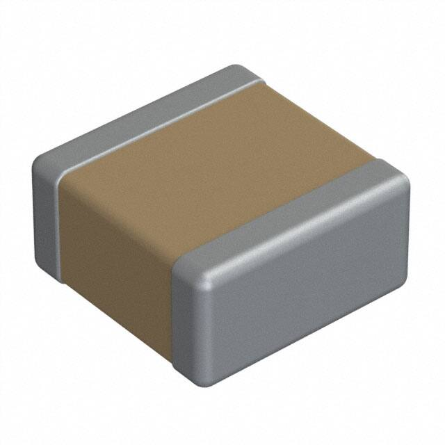


 工商网监
湘ICP备2023018690号
工商网监
湘ICP备2023018690号
