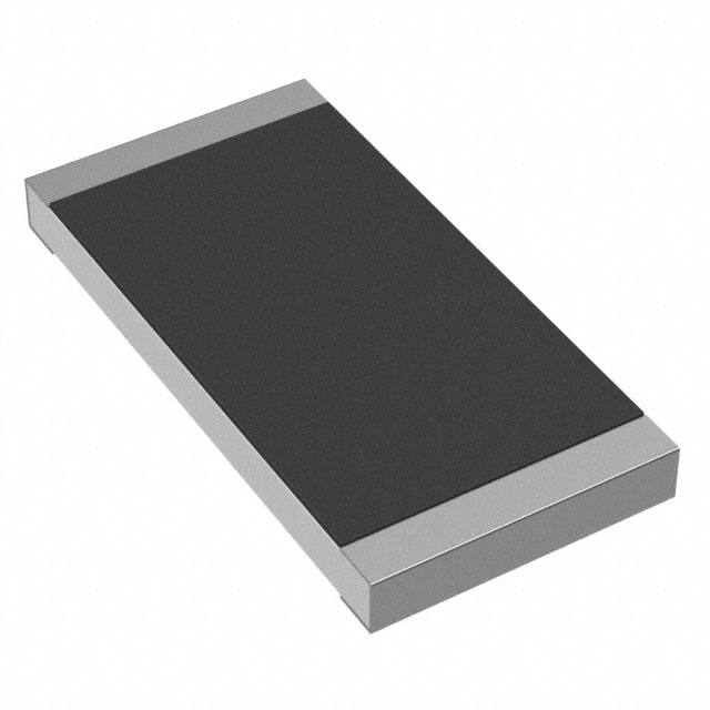
general purpose 2%, 5% tolerance
thick film chip resistor
EU
features
• Products with lead-free terminations
meet EU RoHS requirements. EU RoHS
regulation is not intended for Pb-glass contained
in electrode, resistor element and glass.
• AEC-Q200 Tested: 0201 (1H), 0402 (1E), 0603 (1J),
0805 (2A), 1206 (2B), 1210 (2E), 2010 (2H/W2H),
2512 (3A/W3A/W3A2)
Type*1
dimensions and construction
L
c
c
W
Ni
Plating
t
Protective
Coating
d
100
1H, 1E, 1J, 2A, 2B, 2E,
W2H, W3A (1W)
80
% Rated Power
100
1H, 1E, 1J, 2A, 2B,
2E, W2H, W3A (1W),
W3A2 (2W)
1F
80
60
1H
(0201)
.024±.001 .012±.001 .004±.002 .006±.002 .009±.001
(0.6±0.03) (0.3±0.03) (0.1±0.05) (0.15±0.05) (0.23±0.03)
+.002
.008±.004 .01 -.004
(0.2±0.1)
.02±.002
.014±.002
(0.25 +0.05
-0.1 )
(0.5±0.05)
(0.35±0.05)
(1.0
.01±.004 .012±.0046
(0.25±0.1) (0.3±0.15)
.012±.004 .012±.004
(0.3±0.1) .018±.004
.063±.008 .031±.004 (0.3±0.1)
(1.6±0.2)
(0.8±0.1) .014±.006 .02±.008 (0.45±0.1)
(0.35±0.15) (0.5±0.2)
+.008
.016±.008 .012 -.004 .02±.004
+0.2
(0.4±0.2)
(0.5±0.1)
(0.3 -0.1 )
.079±.008 .049±.004
(2.0±0.2) (1.25±0.1)
.018±.010 .024±.008 .022±.004
(0.45±0.25) (0.6±0.2) (0.55±0.1)
.016 +.008
-.004
.02±.012
.063±.008 (0.5±0.3)
(0.4 +0.2
-0.1 )
.126±.008 (1.6±0.2) .022±.012 .031±.008
(3.2±0.2)
(0.55±0.35) (0.8±0.2)
.102±.008
.016 +.008
(2.6±0.2)
-.004
+.004
-.002
+0.1 )
-0.05
.039
1J
(0603)
1J AT
(0603)
Ceramic
Substrate
Derating Curve
.015±.001 .007±.001 .004±.001 .004±.001 .005±.001
(0.4±0.02) (0.2±0.02) (0.10±0.03) (0.11±0.03) (0.13±0.02)
1E AT
(0402)
Resistive Inner
Film
Electrode
60
2A
(0805)
40
20
40
0
-60
20
-40
-20
0
-55
-55
0
20
40
60
80
100 120 140
70
Ambient Temperature
(°C)
125
160
For resistors operated at an ambient
temperature of 70°C or higher, the
power shall be derated in accordance
with the above derating curve.
40
60
80
100 120
70
Terminal Part Temperature
(°C)
160
140
155
125
80
W3A2
60
2B AT
(1206)
2E
(1210)
40
20
0
-60
-55
-40
-20
0
20
40
60
80
100 120 140
95
Terminal Part Temperature
(°C)
160
155
When the terminal part temperature of the resistor exceeds the rated terminal part
temperature shown above, the power shall be derated according to the derating curve.
Please refer to “Introduction of the derating curves based on the terminal part temperature”
on the beginning of our catalog before use
*1 Parentheses indicate EIA package size codes.
*2 RK73B 2H, 3A and 3A2 are also still available (different “d” dimensions = 0.4 +0.2/-0.1mm)
ordering information
RK73B
2B
Type
Size
1F
1H
1E
1J
2A
2B
2E
W2H
W3A
2H
3A
W3A2
2A AT
(0805)
2B
(1206)
100
155
% Rated Power
0
-60 -40 -20
20
2H
(2010)
W2H*2
(2010)
.197±.008 .098±.008
(2.5±0.2)
(5.0±0.2)
3A*2
(2512)
W3A/W3A2*
(2512)
2
Nil: Standard
New A: Heat shock
resistance *2
*2 With type A only T is available as the terminal surface material.
Termination
Material
T: Sn
G: Au *3
(L: Sn/Pb*4)
(0.4 +0.2
-0.1 )
.024±.004
(0.6±0.1)
.02±.012 .026±.006
(0.5±0.3) (0.65±0.15)
.016 +.008
-.004
(0.4 +0.2
-0.1 )
.248±.008 .122±.008
(6.3±0.2)
(3.1±0.2)
T
Characteristics
t
1F
(01005)
1E
(0402)
Sn
Plating
Dimensions inches (mm)
W
c
d
L
(Inch Size Code)
.026±.006
(0.65±0.15)
TD
Packaging
TX: 4mm width - 1mm pitch
plastic embossed
TBL - TCM: 2mm pitch press
paper
TPL - TP: 2mm pitch punch paper
TD: 4mm pitch punch paper
TE: 4mm pitch plastic embossed
102
J
Nominal
Resistance
2 significant
figures + 1
multiplier
“R” indicates
decimal on
value
很抱歉,暂时无法提供与“RK73B3ATTE563G”相匹配的价格&库存,您可以联系我们找货
免费人工找货