CURRENT SENSING
EU
RoHS
TSL・SL(金属素子タイプ)
・SLN
電流検出用チップ抵抗器
Current Detecting Chip Resistors
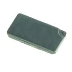
■構造図 Construction
電流検出用面実装抵抗器
Current Detecting Chip Resistors
L
W
b
t
a
①
c
②
③
① モールド樹脂 Molded resin
② 抵抗体
(金属素子) Resistive element (Metal plate)
③ 電極 Electrode
外装色:黒 Coating color:Black
■外形寸法 Dimensions
■特長 Features
●
●
●
●
●
●
●
●
●
●
●
●
●
●
●
●
� 型、超低抵抗値(3mΩ〜)、高精度(±0.5%)のSMD形状の
小
電流検出用抵抗器です。
�難燃性樹脂(UL94 V-0)モールド封止形状です。
�モ ールド成型品のため、寸法精度が良く搭載性、耐衝撃性に
優れています。
�金属端子電極のため、端子強度、はんだ付け性に優れています。
�金属板端子電極構造なので、熱膨張収縮を吸収します。
�フロー、リフロー、コテはんだ付けに対応します。
�端子鉛フリー品は、欧州RoHS対応です。
�AEC-Q200に対応(データ取得)しています。
�SMD type of small size, ultra-low resistance (3mΩ〜) and
high accuracy (±0.5%) resistor for current sensing.
E
� ncapsulated with flame retardant resin molding. (UL94 V-0)
�E xcellent dimension accuracy, mountability and shockresistance due to molded products.
�Excellent terminal strength and solderability due to structure
of a metal plate terminal electrode.
�Easy to absorb the thermal expansion and shrinkage because
of a metal plate terminal structure.
�Suitable for flow, reflow and iron solderings.
��Products with lead free termination meet EU-RoHS
requirements.
�AEC-Q200 qualified.
寸 法 Dimensions(mm)
L±0.3
t±0.2
a±0.2
b±0.2
5.0
6.3
2.5
3.1
1.7
1.0
2.0
2.4
0.9
0.7
1.2±0.3
1.2±0.3
6.3
3.1
1.9
2.4
1.2
1.2±0.3
90
11.5
11.5
7.0
7.0
2.5
2.4
5.0
5.5
1.7
1.6
2.6±0.5
2.55±0.4
476
500
SL07
(2010)
TSL1
(2512)
SL1・SLZ1
(2512)
SL2
(4527)
SLN2
(4527)
Weight( g)
(1000pcs)
W±0.2
c
45
41
■品名構成 Type Designation
例 Example
SL
1
T
TE
10L0
品 種
Product
Code
定格電力
Power
Rating
端子表面材質
Terminal
Surface Material
二次加工
Taping
TSL
SL
SLN
07:0.75W
1:1.0W
2 : 2.0W
T:Sn
TE :Plastic
embossed
BK: Bulk
公称抵抗値
Nominal
Resistance
D,F:4 digits
J,G:3 digits
Ex.
0.1Ω:R10
5mΩ:5L0
※1
抵抗値範囲(Ω)
Resistance Value
3m〜9.1m
10m〜91m
0.1〜0.36
3桁表示
3 digits
3L0〜9L1
10L〜91L
R10〜R36
※1
抵抗値範囲(Ω)
Resistance Value
5m〜9.1m
10m〜91m
0.1〜0.36
F
75
抵抗値許容差
Resistance
Tolerance
抵抗温度係数
T.C.R
(×10−6/K)
D :±0.5%
F : ±1%
G:±2%
J : ±5%
Nil:0~150
0~200
±75(SLN2)
±100
±110
±180
50:±50(SL1)
75:±75(SL1)
4桁表示
4 digits
5L00〜9L10
10L0〜91L0
R100〜R360
端子表面材質は鉛フリーめっき品が標準となります。
環境負荷物質含有についてEU-RoHS以外の物質に対するご要求がある場合にはお問合せください。
テーピングの詳細については巻末のAPPENDIX Cを参照してください。
The terminal surface material lead free is standard.
Contact us when you have control request for environmental hazardous material other than the substance
specified by EU-RoHS.
For further information on taping, please refer to APPENDIX C on the back pages.
■用途 Applications
自動車
ノートPC
電池パック
ACアダプター
DC-DCコンバータ
形名 Type
(Inch Size Code)
Automotive
Note PCs
Battery packs
AC Adapters
DC-DC converters, etc.
■ジャンパー定格 Jumper Ratings
■参考規格 Reference Standards
IEC 60115-1
JIS C 5201-1
形 名
Type
SLZ1
抵抗値
Resistance
0.5mΩ以下
0.5mΩ max.
定格電流
Current Rating
44A
抵抗温度係数
−6
T.C.R.
(×10 /K)
4000以下
4000 max.
■定格 Ratings
定格電力
Power
Rating
SL07
0.75W
−
5m〜100m
−
TSL1
1W
10m〜100m
5m〜100m
−
10m〜102m
5m〜102m
3m、4m
SL1
1W
SL1
(TCR±50ppm)
SL1
(TCR±75ppm)
1W
1W
SL2
2W
SLN2
2W
定格周囲温度
Rated Ambient
Temp.
70℃
定格端子部温度
Rated Terminal
Part Temp.
抵抗値範囲※3
Resistance Range(Ω)
F:±1%
G:±2%
E24・E96※4
E24
形 名
Type
125℃
D:±0.5%
E24・E96※4
34.8m〜200mΩ 34.8m〜200mΩ
20m〜200mΩ 20m〜200mΩ
120℃
−
−
10m〜360mΩ
5m〜360mΩ
3m、4m
5m〜200m
5m〜200m
−
J:±5%
E24
抵抗温度係数
T.C.R.
(×10−6/K)
0〜200:R<11mΩ
0〜150:R≧11mΩ
±180:R<15mΩ
5m〜100m
±100:R≧15mΩ
±180:R<15mΩ
5m〜100m
±100:R≧15mΩ
36m〜200mΩ
±50ppm
20m〜200mΩ
±75ppm
3m〜360mΩ ±180:R<11mΩ
±100:R≧11mΩ
±110:R<10mΩ
5m〜200m
±75:R≧10mΩ
使用温度範囲
Operating Temp.
Range
テーピングと包装数/リール
Taping & Q’
ty/Reel(pcs)
TE
2,000
5m〜100m
3,000
−55℃〜+180℃
1,000
定格電圧は √ ̄ ̄ ̄ ̄ ̄ ̄ ̄ ̄
定格電力×公称抵抗値による算出値、又は表中の最高使用電圧のいずれか小さい値が定格電圧となります。
Rated voltage= √ ̄ ̄ ̄ ̄ ̄ ̄ ̄ ̄ ̄ ̄ ̄
Power Rating×Resistance value or Max. working voltage, whichever is lower.
※3 抵抗値範囲内において、3m、4m、5m、6m、7m、8m、9mΩにも対応致します。 3m, 4m, 5m, 6m, 7m, 8m and 9mΩ are available in each resistance range.
※4 SL07及びSL1
(T.C.R:±50/±75 ppmの内、102mΩ≦R≦200mΩ)
のE96シリーズは適用外
(E24シリーズのみ) SL07 and SL1 (T.C.R: ±50/±75 ppm, 102mΩ≦R≦200mΩ) offer only E24 series.
お客様の使用状況において、定格周囲温度、定格端子部温度のどちらを使用するか疑義が生じる場合は定格端子部温度を優先してください。
詳細は14〜17頁の「端子部温度の負荷軽減曲線の紹介」をご参照ください。
If any questions arise whether to use the“Rated Ambient Temperature”or the“Rated Terminal Part Temperature”in your usage conditions, please give priority to the“Rated Terminal Part Temperature”.
For more details, please refer to“Introduction of the derating curves based on the terminal part temperature”in page 14 to 17.
本カタログに掲載の仕様は予告なく変更する場合があります。ご注文およびご使用前に納入仕様書で内容をご確認ください。
Oct. 2017
車載機器、医療機器、航空機器など人命に関わったり、あるいは甚大な損害を引き起こす可能性のある機器へのご使用を検討される場合には、必ず事前にご相談ください。
Specifications given herein may be changed at any time without prior notice. Please confirm technical specifications before you order and/or use.
Contact our sales representatives before you use our products for applications including automotives, medical equipment and aerospace equipment.
www.koaglobal.com
Malfunction or failure of the products in such applications may cause loss of human life or serious damage.
�80
定格電力比(%)
80
60
40
20
Percent rated power
100
Percent rated power
100
SLN2
60
SL07, TSL, SL1, SL2
40
20
0
-60 -40 -20 0 20 40 60 80 100 120 140 160 180
-55
70
周囲温度 Ambient temperature(℃)
0
-60 -40 -20 0 20 40 60 80 100 120 140 160 180
-55
125
端子部温度 Terminal part temperature
(℃)
周囲温度 70℃以上で使用される場合は、上図負荷軽減曲線に従っ
て、定格電力を軽減して御使用ください。
For resistors operated at an ambient temperature of 70℃ or
above, a power rating shall be derated in accordance with the
above derating curve.
上記の端子部温度以上で使用される場合は、負荷軽減曲線に従っ
て定格電力を軽減してご使用ください。
※�ご 使用方法につきましては巻頭の“端子部温度の負荷軽減曲線
の紹介”を参照願います。
For resistors operated terminal part temperature of described for
each size or above a power rating shall be derated in accordance
with derating curve.
※ �Please refer to“Introduction of the derating curve based on the
terminal part temperature”on the beginning of our catalog
before use.
■温度上昇 Temperature Rise
175
温度上昇(℃)
Temperature rise
150
150
②
①
75
50
※ 33mΩ
10mm pattern
25
0
0
25
50
75
定格電力比率 Power rating(%)
200
SLN2
TSL1
SLN2
TSL1
175
125
100
TSL1/SLN2
200
②
②
①
①
温度上昇(℃)
Temperature rise
SL2
SL1
SL2
SL1
100
②
②
①
①
②
①
75
50
※ TSL1:20mΩ
SLN2:110mΩ
10mm pattern
25
0
0
25
50
75
定格電力比率 Power rating(%)
SL07 ②
SL07 ①
150
125
100
SL07
175
温度上昇(℃)
Temperature rise
SL1/SL2
200
電流検出用面実装抵抗器
Current Detecting Chip Resistors
定格電力比(%)
■負荷軽減曲線 Derating Curve
100
125
100
②
75
①
50
25
0
※ 20mΩ
10mm pattern
0
25
50
75
定格電力比率 Power rating(%)
100
温度上昇については、弊社測定条件下で測定しているため、使用状況、使用基板により数値が異なりますので、ご使用に際しては別途お問い合わせください。
Regarding the temperature rise, the value of the temperature varies per conditions and board for use since the temperature is measured under our measuring
conditions. Please refer to us before use.
■性能 Performance
試験項目
Test Items
規格値 Performance Requirements
ΔR±%
試験方法
Test Methods
保証値 Limit
代表値 Typical
抵抗値
Resistance
規定の許容差内
Within specified tolerance
—
25℃
抵抗温度係数
T.C.R.
規定値内
Within specified T.C.R.
—
+25℃ / +125℃
過負荷(短時間)
Overload(Short time)
1:SL07, TSL1, SL1, SL2
0.5:SLN2
1:SL07, TSL1, SL1, SL2
0.25:SLN2
はんだ耐熱性
Resistance to soldering heat
1:SL07, TSL1, SL1, SL2
1:SL07, TSL1, SL1, SL2
0.5:SLN2
0.5:SLN2
温度急変
Rapid change of temperature
1:SL07, TSL1, SL1, SL2
0.5:SL07, TSL1, SL1, SL2
−55℃(30min.)/+150℃(30min.)100 cycles
0.5:SLN2
0.25:SLN2
2:SL07, TSL1, SL1, SL2
0.5:SL07, TSL1, SL1, SL2
0.5:SLN2
0.25:SLN2
70℃での耐久性
Endurance at 70℃
2:SL07, TSL1, SL1, SL2
1:SLN2
1
−55℃(15min.)/+150℃(15min.)1000 cycles
40℃±2℃, 90%〜95%RH, 1000h
1.5時間 ON/0.5時間 OFF の周期 1.5h ON/0.5h OFF cycle
85℃±2℃, 85%RH±3%RH, 1000h
定格電力×0.1倍 Rated power×0.1
70℃±2℃, 1000h
1.5時間 ON/0.5時間 OFF の周期 1.5h ON/0.5h OFF cycle
低温放置
Low temperature exposure
0.5
0.25
耐湿負荷
Moisture resistance
SL07:定格電力×4倍を5秒印加 Rated power×4 for 5s
TSL1:定格電力×2.5倍を5秒印加 Rated power×2.5 for 5s
SL1, SL2, SLN2:定格電力×5倍を5秒印加 Rated power×5 for 5s
SL1(T.C.R:±50/±75)は定格電力×4倍を5秒印加
SL1(T.C.R:±50/±75)
:Rated power×4 for 5s
260℃±5℃, 10s±1s
( )
260℃±5℃, 10s〜12s
SL07, TSL1, SL1, SL2:ー55℃, 1h
SLN2:ー65℃, 24h
■使用上の注意 Precautions for Use
� ャント抵抗としてご使用になる場合、周囲のコイルとの電磁誘導を考慮してパターンレイアウトをしてください。
シ
� 0mΩ以下の抵抗値においては、ランドパターンの大きさや接続はんだの量により、はんだ付け後の抵抗値が変動する事があります。事前に抵抗
5
値低下・上昇の影響をご確認の上、機器設計してください。
● I
� n case of using the low ohm resistors as shunt resistors, please lay out a pattern considering the electromagnetic induction with surrounding inductors.
● I
� n the resistance values of 50mΩ or under, the resistance value after soldering may change depending on the size of pad pattern or solder amount.
Make sure the effect of decline/increase of resistance value before designing.
●
●
本カタログに掲載の仕様は予告なく変更する場合があります。ご注文およびご使用前に納入仕様書で内容をご確認ください。
Oct. 2017
車載機器、医療機器、航空機器など人命に関わったり、あるいは甚大な損害を引き起こす可能性のある機器へのご使用を検討される場合には、必ず事前にご相談ください。
Specifications given herein may be changed at any time without prior notice. Please confirm technical specifications before you order and/or use.
Contact our sales representatives before you use our products for applications including automotives, medical equipment and aerospace equipment.
www.koaglobal.com
Malfunction or failure of the products in such applications may cause loss of human life or serious damage.
�