Programming Cables
User Guide
FPGA-UG-02042 Version 26.0
April 2018
�Programming Cables
User Guide
Contents
1. Features ................................................................................................................................................................. 4
2. Programming Cables .............................................................................................................................................. 4
3. Programming Cable Pin Definitions ......................................................................................................................... 5
4. Programming Software ........................................................................................................................................... 7
5. Target Board Design Considerations ....................................................................................................................... 7
6. Programming Flywire and Connection Reference .................................................................................................... 8
7. Connecting the Programming Cable ...................................................................................................................... 10
8. Programming Cable TRST Pin ................................................................................................................................ 10
9. Programming Cable ispEN Pin ............................................................................................................................... 10
10. Ordering Information ........................................................................................................................................... 11
Appendix A. Troubleshooting the USB Driver Installation ............................................................................................. 12
Technical Support ....................................................................................................................................................... 16
Revision History .......................................................................................................................................................... 16
© 2009-2018 Lattice Semiconductor Corp. All Lattice trademarks, registered trademarks, patents, and disclaimers are as listed at www.latticesemi.com/legal.
All other brand or product names are trademarks or registered trademarks of their respective holders. The specifications and information herein are subject to change without notice.
2
FPGA-UG-02042-26.0
�Programming Cables
User Guide
Figures
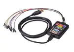
Figure 1.1. USB Cable – HW-USBN-2B ............................................................................................................................ 4
Figure 3.1. Programming Cable In-System Programming Interface for the PC (HW-USBN-2B)* ....................................... 5
Figure 3.2. Programming Cable In-System Programming Interface for the PC (HW-USB-1A or HW-USB-2A)* .................. 6
Figure 3.3. Programming Cable In-System Programming Interface for the PC (HW-DLN-3C and Equivalents)*................. 6
Figure 3.4. Programming Cable In-System Programming Interface for the PC (pDS4102-DL2 or pDS4102- DL2A) ............ 6
Figure 3.5. Programming Cable In-System Programming Interface for the PC (HW7265-DL2 or HW7265-DL2A)* ............ 6
Figure A.1. Device Manager ......................................................................................................................................... 12
Figure A.2. Unknown Device Properties ....................................................................................................................... 12
Figure A.3. Update Driver Software.............................................................................................................................. 13
Figure A.4. Lattice EzUSB Driver ................................................................................................................................... 13
Figure A.5. FTDI FTUSB Driver ...................................................................................................................................... 13
Figure A.6. Windows Security ...................................................................................................................................... 14
Figure A.7. USB Installation Completed ........................................................................................................................ 14
Figure A.8. Installation Completed ............................................................................................................................... 14
Figure A.9. Installation Completed ............................................................................................................................... 15
Tables
Table 3.1. Programming Cable Pin Definitions ................................................................................................................ 5
Table 6.1. Pin and Cable Reference ................................................................................................................................ 8
Table 10.1. Programming Cable Feature Summary ....................................................................................................... 11
Table 10.2. Ordering Information................................................................................................................................. 11
© 2009-2018 Lattice Semiconductor Corp. All Lattice trademarks, registered trademarks, patents, and disclaimers are as listed at www.latticesemi.com/legal. All other brand or product names are
trademarks or registered trademarks of their respective holders. The specifications and information herein are subject to change without notice.
FPGA-UG-02042-26.0
3
�Programming Cables
User Guide
1. Features
Support for all Lattice programmable products
1.2 V to 3.3 V programming (HW-USBN-2B)
1.2 V to 5 V programming (All other cables)
Ideal for design prototyping and debugging
Connect to multiple PC interfaces
USB (v.1.0, v.2.0)
PC Parallel Port
Easy-to-use programming connectors
Versatile flywire, 2 x 5 (.100”) or 1 x 8 (.100”) connectors
6 feet (2 meters) or more of programming cable length (PC to DUT)
Lead-free/RoHS compliant construction
Figure 1.1. USB Cable – HW-USBN-2B
2. Programming Cables
Lattice Programming Cable products are the hardware connection for in-system programming of all Lattice devices.
After you complete your logic design and create a programming file with the Lattice Diamond®/ispLEVER® Classic
development tools, you can use Diamond Programmer or ispVM™ System software ispVM™ System software or
Diamond Programmer to program devices on your board. The ispVM System/Diamond Programmer software
automatically generates the appropriate programming commands, programming addresses and programming data
based on information stored in the programming file and parameters you set in Diamond Programmer/ispVM System.
Programming signals are then generated from the USB or parallel port of a PC and directed through the Programming
Cable to the device. No additional components are required for programming.
Diamond Programmer/ispVM System software is included with all Lattice design tool products and is available for
download from the Lattice web site at www.latticesemi.com/software.
© 2009-2018 Lattice Semiconductor Corp. All Lattice trademarks, registered trademarks, patents, and disclaimers are as listed at www.latticesemi.com/legal.
All other brand or product names are trademarks or registered trademarks of their respective holders. The specifications and information herein are subject to change without notice.
4
FPGA-UG-02042-26.0
�Programming Cables
User Guide
3. Programming Cable Pin Definitions
The functions provided by the Programming cables correspond with available functions on Lattice programmable
devices. Since some devices contain different programming features, the specific functions provided by the
Programming cable may depend on the selected target device. ispVM System/Diamond Programmer software will
automatically generate the appropriate functions based on the selected device. See Table 3.1 for an overview of the
Programming cable functions.
Table 3.1. Programming Cable Pin Definitions
Programming Cable Pin
VCC
Name
Programming
Voltage
Programming Cable Pin Type
Input
TDO/SO
Test Data
Output
TDI/SI
Test Data Input
Output
ispEN/PROG/SN
Enable
Output
Enable device to be programmed.
SN = SSPI Chip select for HW-USBN-2B
TRST
DONE
TMS
Test Reset
DONE
Test Mode
Select Input
Output
Input
Output
Optional IEEE 1149.1 state machine reset.
DONE indicates status of configuration
Used to control the IEEE1149.1 state machine.
GND
Ground
Input
Connect to ground plane of the target device
TCK/SCLK
INIT
Test Clock Input
Initialize
Output
Input
Used to clock the IEEE1149.1 state machine
Indicates device is ready for configuration to
begin. INITN is only found on some devices.
I2C: SCL1
I2C: SDA1
I2C SCL
I2C SDA
Output
Output
5V Out1
5 V Out
Output
Provides the I2C signal SCL
Provides the I2C signal SDA.
Provides a 5 V signal for the iCEprog M1050
Programmer.
Input
Description
Connect to VCC or VCCJ plane of the target device.
Typical ICC = 10 mA. Your board design supplies
the power for VCC. Note: This may not be the
same as a target device’s VCCO plane.
Used to shift data out via the IEEE1149.1 (JTAG)
programming standard.
Used to shift data in via the IEEE1149.1
programming standard.
*Note: Only found on the HW-USBN-2B cable.
TCK/SCLK *
TMS *
I2C: SCL
TDI/SI *
5 V OUT
TDO/SO *
I2C: SDA
VCC *
DONE
GND *
ISPEN/PROG/SN
TRST
* Indicates flywire connections required for most basic JTAG programming.
Figure 3.1. Programming Cable In-System Programming Interface for the PC (HW-USBN-2B)*
*Note: Requires Diamond Programmer 3.1 or later.
© 2009-2018 Lattice Semiconductor Corp. All Lattice trademarks, registered trademarks, patents, and disclaimers are as listed at www.latticesemi.com/legal. All other brand or product names are
trademarks or registered trademarks of their respective holders. The specifications and information herein are subject to change without notice.
FPGA-UG-02042-26.0
5
�Programming Cables
User Guide
Function
To PC
®
61
HW-USB-1A
Color
V CC
SDO/TDO
SDI/TDI
ispEN/Enable/PROG
TRST/DONE
Red
Brown
Orange
Yellow
Gree n
MODE/TMS
GND
Purple
Black
SCLK/TCK
IN IT
W hite
Blue
To System
Board
Figure 3.2. Programming Cable In-System Programming Interface for the PC (HW-USB-1A or HW-USB-2A)*
*Note: Lattice PAC-Designer® software does not support programming with USB cables. To program ispPAC devices with these cables,
use the Diamond Programmer/ispVM System software.
HW7265-DL3 and HW7265-DL3A – Grey Housing with RJ-45 Connector
Other Cables are Labeled with Part Number
To PC
25-pin
Parallel
Port
Adapter
Function
V CC
61
Color
Red
SDO/TDO
Brown
SDI/TDI
Orange
ispEN/Enable/Prog
Yellow
TRST
Green
MODE/TMS
Purple
GND
Black
SCLK/TCK
White
To
System
Board
Figure 3.3. Programming Cable In-System Programming Interface for the PC (HW-DLN-3C and Equivalents)*
*Note: HW7265-DL3, HW7265-DL3A, HW-DL-3B, HW-DL-3C and HW-DLN-3C are functionally equivalent products.
End View
pDS4102-DL2 – Blue Housing
pDS4102-DL2A – Grey Housing
To PC
25-pin
Parallel
Port
Adapter
.100" Center-Spacing
Eight Positions
RJ-45 Connector
Eight Positions
.01 f*
Capacitor
6'
Function
V CC
Pin #
1
SDO/TDO
2
SDI/TDI
3
ispEN/Enable/PROG
4
TRST
5
MODE/TMS
6
GND
7
SCLK/TCK
8
To System
Board
Note: Capacitor Recommended on System Board
Figure 3.4. Programming Cable In-System Programming Interface for the PC (pDS4102-DL2 or pDS4102- DL2A)
Figure 3.5. Programming Cable In-System Programming Interface for the PC (HW7265-DL2 or HW7265-DL2A)*
*Note: For reference purposes, the 2 x 10 connector on the HW7265-DL2 or HW7265-DL2A is equivalent to Tyco 102387-1. This will
interface to standard 100-mil spacing 2 x 5 headers, or a 2 x 5 keyed, recessed male connector such as the 3M N2510-5002RB.
© 2009-2018 Lattice Semiconductor Corp. All Lattice trademarks, registered trademarks, patents, and disclaimers are as listed at www.latticesemi.com/legal.
All other brand or product names are trademarks or registered trademarks of their respective holders. The specifications and information herein are subject to change without notice.
6
FPGA-UG-02042-26.0
�Programming Cables
User Guide
4. Programming Software
Diamond Programmer and ispVM System for Classic devices is the preferred programming management software tool
for all Lattice devices and download cables. The latest version of Lattice Diamond Programmer or ispVM System
software is available for download from the Lattice web site at www.latticesemi.com/software.
5. Target Board Design Considerations
A 4.7K pull-down resistor is recommended on the TCK connection of the target board. This pull-down is recommended
to avoid inadvertent clocking of the TAP controller induced by fast clock edges or as VCC ramps up. This pull-down is
recommended for all Lattice programmable families.
The I2C signals SCL and SDA are open drain. A 2.2K pull-up resistor to VCC is required on the target board.
For Lattice device families that feature low power, it is recommended to add a 500 Ohm resistor between VCCJ and
GND during the programming interval when a USB Programming cable is connected to a very low power board design.
A FAQ is available that discusses this in more depth at:
http://www.latticesemi.com/en/Support/AnswerDatabase/2/2/0/2205
The JTAG programming port speed may need to be governed when using the Programming cables connected to
customer PCBs. This is especially important when there is long PCB routing or with many daisy-chained devices. The
Lattice programming software can adjust the timing of TCK applied to the JTAG programming port from the cable. This
low-precision port setting of TCK depends on many factors, including the PC speed and the type of cable used (parallel
port, USB or USB2). This software feature provides an option to slow the TCK for debug or noisy environments. A FAQ is
available that discusses this in more depth at: http://www.latticesemi.com/en/Support/AnswerDatabase/9/7/974.aspx
The USB Download Cable can be used to program Power Manager or ispClock products with Lattice programming
software. When using the USB cable with the Power Manager I devices, (POWR604, POWR1208, POWR1208P1), you
must slow do TCK by a factor of 2. A FAQ is available that discusses this in more depth at:
http://www.latticesemi.com/en/Support/AnswerDatabase/3/0/306.aspx
© 2009-2018 Lattice Semiconductor Corp. All Lattice trademarks, registered trademarks, patents, and disclaimers are as listed at www.latticesemi.com/legal. All other brand or product names are
trademarks or registered trademarks of their respective holders. The specifications and information herein are subject to change without notice.
FPGA-UG-02042-26.0
7
�Programming Cables
User Guide
6. Programming Flywire and Connection Reference
Refer to Table 6.1 to identify, per Lattice device, how to connect various Lattice Programming Cable Flywires. JTAG, SPI and I2C configuration ports are
unambiguously identified. Legacy cables and hardware are included for reference. In addition, various header configurations are tabulated.
Table 6.1. Pin and Cable Reference
HW-USBN-2B
Flywire color
HW-USBN-2A
Flywire color
HW-DLN-3C
Flywire color
Programming cable pin type
Target Board
Recommendation
JTAG Port Devices
ECP5™
LatticeECP3™ /
LatticeECP2M™/LatticeECP2™
/ LatticeECP™/LatticeEC™
LatticeXP2™ / LatticeXP™
LatticeSC™/LatticeSCM™
MachXO2™/MachXO3™
MachXO™
ORCA®/FPSC
ispXPGA® / ispXPLD™
ispMACH® 4000/
ispMACH/ispLSI® 5000
MACH®4A
ispGDX2™
ispClock™ (Note 4)
Platform Manager™ / Power
Manager / Power Manager II
(Note 4)
ispPAC®
Slave SPI Port Devices
ECP5™
LatticeECP3™
MachXO2™/MachXO3™
CrossLink™ LIF-MD6000
iCE40™/iCE40LM/iCE40
Ultra™/iCE40 UltraLite™
I2C Port Devices
MachXO2™/MachXO3™
Power Manager II
ASC
CrossLink™ LIF-MD6000
Headers
1 x 10 conn (various cables)
1 x 8 conn (see Fig 5)
2 x 5 conn (see Fig 6)
Programmers
Model 300
iCEprog M1050
TDI/SI
Orange
TDI
Orange
TDI
Orange
Output
TDO/SO
Brown
TDO
Brown
TDO
Brown
Input
TMS
Purple
TMS
Purple
TMS
Purple
Output
4.7 kOhm
Pull-Up
TCK/SCLK ISPEN/PROG
DONE
TRST(OUTPUT)
VCC
GND
I2C: SCL
White
Yellow
Blue
Green
Red
Black
Yellow/White
TCK
ispEN/PROG
INIT
TRST(OUTPUT)/DONE(INPUT)
VCC
GND
White
Yellow
Blue
Green
Red
Black
TCK
ispEN/PROG
na
TRST(OUTPUT)
VCC
GND
White
Yellow
Green
Red
Black
Output
Output
Input
Input/Output
Input
Input
Output
4.7 kOhm Pull- (Note 1)
(Note 2)
(Note 3)
Down
Connect the Programming Cable wires (above) to the corresponding Device or Header pins (below)
TDI
TDI
TDO
TDO
TMS
TMS
TCK
TCK
Required Required
Required Required
TDI
TDI
TDI
TDI
TDI
TDI
TDI
TDO
TDO
TDO
TDO
TDO
TDO
TDO
TMS
TMS
TMS
TMS
TMS
TMS
TMS
TCK
TCK
TCK
TCK
TCK
TCK
TCK
Required
Required
Required
Required
Required
Required
Required
TDI
TDI
TDI
TDI
TDO
TDO
TDO
TDO
TMS
TMS
TMS
TMS
TCK
TCK
TCK
TCK
Required
Required
Required
Required
TDI
TDO
TMS
TCK
MOSI
MOSI
SO
MOSI
SPI_SI
MOSI
MOSI
SI
MOSI
SPI_SO
—
—
—
—
—
CCLK
CCLK
CCLK
SPI_SCK
SPI_SCK
—
—
—
—
—
—
—
—
—
—
—
—
—
—
—
—
3
3
5
2
2
7
6
6
3
8
8
1
4
4
10
9 or 10
—
—
5 or 9
5
9
5
8
7
5
3
—
1
7
10
9
—
3
9
1
Optional Connections to device ispEN, PROGRAMN,
INITN, DONE and/or TRST signals
(Define in Custom I/O settings in ispVM System
or Diamond Programmer software.
Not all devices have these pins available)
SN
SN
SN
SPI_SS
SPI_SS_B
Optional Connections to device
PROGRAMN, INITN and/or DONE signals
Opt. CDONE
CRESET_B
Opt. CDONE
CRESET_B
Optional Connections to device PROGRAMN, INITN
and/or DONE signals
—
—
—
Opt. CDONE
—
—
I2C: SDA
Green/White
na
5V Out
Red/White
na
Output
(Note 3)
Output
—
—
—
—
—
—
Required
Required
Required
Required
Required
Required
Required
—
—
—
—
—
—
—
—
—
—
—
—
—
—
—
—
—
—
—
—
—
Required
Required
Required
Required
—
—
—
—
—
—
—
—
—
—
—
—
Required Required
—
—
—
Required
Required
Required
Required
Required
Required
Required
Required
Required
Required
—
—
—
—
—
—
—
—
—
—
—
—
—
—
—
Required
Required
Required
Required
Required
SCL
SDA
Required SCL_M + SCL_S SCL_M + SCL_M
Required
SCL
SDA
Required
SCL
SDA
—
—
—
—
1
1
6
7
7
2, 4,or 8
—
—
—
—
—
—
—
—
—
6
6
2, 4,or 8
10
—
—
—
—
—
4 (Note 5)
© 2009-2018 Lattice Semiconductor Corp. All Lattice trademarks, registered trademarks, patents, and disclaimers are as listed at www.latticesemi.com/legal.
All other brand or product names are trademarks or registered trademarks of their respective holders. The specifications and information herein are subject to change without notice.
8
FPGA-UG-02042-26.0
�Programming Cables
User Guide
Notes:
1. For older Lattice ISP devices, a 0.01 μF decoupling capacitor is required on ispEN/ENABLE of the target board.
2. For HW-USBN-2A/2B, the target board supplies the power - Typical ICC = 10 mA. For devices that have a VCCJ pin, the VCCJ must be connected to the cable’s VCC. For other
devices, connect the appropriate bank VCCIO to the cable's VCC. A 0.1 μF decoupling capacitor is required on VCCJ or VCCIO close to the device. Please refer to the device data
sheet to determine if the device has a VCCJ pin or what VCCIO bank governs the target programming port (this may not be the same as a target device’s core VCC/VSS plane).
3. Open drain signals. External pull-up ~2.2 kOhm resistor to the appropriate bank VCCIO or VCCJ is required.
4. When using PAC-Designer® software to program ispPAC devices, do not connect TRST/DONE.
5. If using a cable older than HW-USBN-2B, connect a +5 V external supply between iCEprog M1050 pin 4 (VCC) and pin 2 (GND).
© 2009-2018 Lattice Semiconductor Corp. All Lattice trademarks, registered trademarks, patents, and disclaimers are as listed at www.latticesemi.com/legal.
All other brand or product names are trademarks or registered trademarks of their respective holders. The specifications and information herein are subject to change without notice.
FPGA-UG-02042-26.0
9
�Programming Cables
User Guide
7. Connecting the Programming Cable
The target board must be un-powered when connecting, disconnecting, or reconnecting the Programming Cable.
Always connect the Programming Cable’s GND pin (black wire) before connecting any other JTAG pins. Failure to follow
these procedures can result in damage to the target programmable device.
8. Programming Cable TRST Pin
Connecting the board TRST pin to the cable TRST pin is not recommended. Instead, connect the board TRST pin to Vcc.
If the board TRST pin is connected to the cable TRST pin, instruct ispVM/Diamond Programmer to drive the TRST pin
high.
To configure ispVM/Diamond Programmer to drive TRST pin high:
1.
Select the Options menu item.
2.
Select Cable and I/O Port Setup.
3.
Select the TRST/Reset Pin Connected checkbox.
4.
Select the Set High radio button.
If the proper option is not selected, the TRST pin will be driven low by ispVM/Diamond Programmer. Consequently, the
BSCAN chain will not work because the chain will be locked into RESET state.
9. Programming Cable ispEN Pin
The following pins should be grounded:
BSCAN pin of the 2000VE devices
ENABLE pin of MACH4A3/5-128/64, MACH4A3/5-64/64 and MACH4A3/5-256/128 devices.
However, the user has the option of having the BSCAN and ENABLE pins driven by the ispEN pin from the cable. In this
case, ispVM/Diamond Programmer must be configured to drive the ispEN pin low as follows:
To configure ispVM/Diamond Programmer to drive ispEN pin low:
1.
Select the Options menu item.
2.
Select Cable and I/O Port Setup.
3.
Select the ispEN/BSCAN Pin Connected checkbox.
4.
Select the Set Low radio button.
Each Programming Cable ships with two small connectors that help you keep the flywires organized. The following
manufacturer and part number is one possible source for equivalent connectors:
1 x 8 Connector (e.g. Samtec SSQ-108-02-T-S)
2 x 5 Connector (e.g. Samtec SSQ-105-02-T-D)
The Programming Cable flywire or headers are intended to connect to standard 100-mil spacing headers (pins spaced
0.100 inch apart). Lattice recommends a header with length of 0.243 inches or 6.17 mm. Though, headers of other
lengths may work equally well.
© 2009-2018 Lattice Semiconductor Corp. All Lattice trademarks, registered trademarks, patents, and disclaimers are as listed at www.latticesemi.com/legal.
All other brand or product names are trademarks or registered trademarks of their respective holders. The specifications and information herein are subject to change without notice.
10
FPGA-UG-02042-26.0
�Programming Cables
User Guide
10. Ordering Information
Table 10.1. Programming Cable Feature Summary
Feature
HW-USBN-2B
HW-USBN-2A
HW-USB-2A
HW-USB-1A
HW-DLN-3C
HW7265-DL3, HW7265-DL2
HW7265-DL3A,
HW-DL-3B,
HW-DL-3C
HW7265-DL2A PDS4102-DL2
PDS4102-DL2A
USB
X
X
X
X
—
—
—
—
—
—
PC-Parallel
1.2 V Support
1.8 V Support
2.5-3.3 V
Support
—
X
X
—
X
X
—
X
X
—
—
X
X
—
X
X
—
X
X
—
—
X
—
X
X
—
—
X
—
X
X
X
X
X
X
X
X
X
X
X
5.0 V Support
2 x 5 Connector
—
—
X
X
X
X
X
X
X
X
X
X
X
X
X
X
X
—
X
—
X
X
X
X
X
X
X
—
X
X
—
X
X
X
X
X
—
—
—
—
—
—
—
X
—
—
X
—
—
X
—
—
—
X
—
—
—
—
—
1 x 8 Connector
Flywire
Lead-free
Construction
Available for
order
Table 10.2. Ordering Information
Description
Ordering Part
Number
China RoHS Environment- Friendly
Use Period (EFUP)
Programming cable (USB). Contains 6' USB cable, flywire
HW-USBN-2B
connectors, 8-position (1 x 8) adapter and 10-position (2 x 5)
adapter, lead-free, RoHS compliant construction.
Programming cable (PC only). Contains parallel port adapter, 6'
HW-DLN-3C
cable, flywire connectors, 8-position (1 x 8) adapter and 10position (2 x 5) adapter, lead-free, RoHS compliant construction.
*Note: Additional cables are described in this document for legacy purposes only, these cables are no longer produced. The cables
currently available for order are fully equivalent replacement items.
© 2009-2018 Lattice Semiconductor Corp. All Lattice trademarks, registered trademarks, patents, and disclaimers are as listed at www.latticesemi.com/legal.
All other brand or product names are trademarks or registered trademarks of their respective holders. The specifications and information herein are subject to change without notice.
FPGA-UG-02042-26.0
11
�Programming Cables
User Guide
Appendix A. Troubleshooting the USB Driver Installation
It is essential that you install the drivers before connecting your PC to the USB cable. If the cable is connected before
installing the drivers, Windows will try to install its own drivers that may not work.
If you have attempted to connect the PC to the USB cable without first installing the appropriate drivers, or have
trouble communicating with the Lattice USB cable after installing the drivers, follow the steps below:
1.
Plug in the Lattice USB cable. Choose Start > Settings > Control Panel > System.
2.
In the System Properties dialog box, click the Hardware tab and Device Manager button. Under Universal Serial Bus
controllers, you should see Lattice USB ISP Programmer. If you do not see this, look for the Unknown Device with
the yellow flag. Double click on the Unknown Device icon.
Figure A.1. Device Manager
3.
In the Unknown device Properties dialog box, click Reinstall Driver.
Figure A.2. Unknown Device Properties
4.
Select Browse my computer for driver software.
© 2009-2018 Lattice Semiconductor Corp. All Lattice trademarks, registered trademarks, patents, and disclaimers are as listed at www.latticesemi.com/legal.
All other brand or product names are trademarks or registered trademarks of their respective holders. The specifications and information herein are subject to change without notice.
12
FPGA-UG-02042-26.0
�Programming Cables
User Guide
Figure A.3. Update Driver Software
Browse to the isptools\ispvmsystem directory for the Lattice EzUSB driver.
Figure A.4. Lattice EzUSB Driver
Browse to the isptools\ispvmsystem\Drivers\FTDIUSBDriver directory for the FTDI FTUSB driver.
Figure A.5. FTDI FTUSB Driver
© 2009-2018 Lattice Semiconductor Corp. All Lattice trademarks, registered trademarks, patents, and disclaimers are as listed at www.latticesemi.com/legal.
All other brand or product names are trademarks or registered trademarks of their respective holders. The specifications and information herein are subject to change without notice.
FPGA-UG-02042-26.0
13
�Programming Cables
User Guide
5.
For Diamond installations, browse to lscc/diamond/data/vmdata/drivers. Click Next.
6.
Select Install this Driver software anyway. The system will update the driver.
Figure A.6. Windows Security
7.
Click Close and finish installing the USB driver.
Figure A.7. USB Installation Completed
8.
Under Control Panel >System >Device Manager > Universal Serial Bus Controllers should include the following:
For the Lattice EzUSB Driver: Lattice USB ISP Programmer device installed.
Figure A.8. Installation Completed
© 2009-2018 Lattice Semiconductor Corp. All Lattice trademarks, registered trademarks, patents, and disclaimers are as listed at www.latticesemi.com/legal.
All other brand or product names are trademarks or registered trademarks of their respective holders. The specifications and information herein are subject to change without notice.
14
FPGA-UG-02042-26.0
�Programming Cables
User Guide
For the FTDI FTUSB Driver: USB Serial Converter A and Converter B devices installed.
Figure A.9. Installation Completed
If you are experiencing problems or need additional information, contact Lattice Technical Support.
© 2009-2018 Lattice Semiconductor Corp. All Lattice trademarks, registered trademarks, patents, and disclaimers are as listed at www.latticesemi.com/legal.
All other brand or product names are trademarks or registered trademarks of their respective holders. The specifications and information herein are subject to change without notice.
FPGA-UG-02042-26.0
15
�Programming Cables
User Guide
Technical Support
For assistance, submit a technical support case at www.latticesemi.com/techsupport.
Revision History
Date
Version
April 2018
26.0
Change Summary
Changed document number from UG48 to FPGA-UG-02024.
Updated document template.
Revised Programming Cables section. Removed redundant information and changed
link to www/latticesemi.com/software.
Updated Programming Cable Pin names in Table 3.1. Programming Cable Pin
Definitions.
Updated Programming Flywire and Connection Reference Section.
Replaced Table 2. Flywire Conversion Reference and Table 3 Recommended Pin
Connections with a single Table 6.1 Pin and Cable Reference.
Moved Table 10.1. Programming Cable Feature Summary under Ordering Information.
November 2016
25.0
Updated Programming Flywire and Connection Reference section.
Revised Table 3, Recommended Pin Connections. Added CrossLink device.
October 2015
24.9
Updated Programming Flywire and Connection Reference section.
Revised Table 3, Recommended Pin Connections. Added CRESET-B column.
Added iCE40 UltraLite device.
Updated Technical Support Assistance section.
March 2015
24.8
Updated Programming Cable Pin Definitions section.
Revised description of INIT in Table 1, Programming Cable Pin Definitions.
January 2015
24.7
Updated Programming Cable Pin Definitions section.
In Table 1, Programming Cable Pin Definitions, ispEN/Enable/PROG changed to
ispEN/Enable/PROG/SN and its description revised.
Updated Figure 2, Programming Cable In-System Programming Interface for the
PC (HW-USBN-2B).
Updated Programming Cable ispEN Pin section.
In Table 4, Programming Cable Feature Summary, HW-USBN-2B marked as available
for order.
Updated Ordering Information section. HW-USBN-2A changed to HW- USBN-2B
July 2014
24.6
Changed document title to Programming Cables User’s Guide
Changed ispDOWNLOAD Cables to Programming Cables.
Updated Target Board Design Considerations section. Updated FAQ link on ispVM tool
control of TCK duty cycle and/or frequency.
Updated Table 3, Recommended Pin Connections. Added ECP5, iCE40LM, iCE40 Ultra,
and MachXO3 device families.
Updated Technical Support Assistance information.
October 2012
24.5
Added iCE40 configuration port pin names to the Flywire Conversion Reference table.
Added iCE40 information to Recommended Cable Connections table.
February 2012
24.4
Updated document with new corporate logo.
© 2009-2018 Lattice Semiconductor Corp. All Lattice trademarks, registered trademarks, patents, and disclaimers are as listed at www.latticesemi.com/legal.
All other brand or product names are trademarks or registered trademarks of their respective holders. The specifications and information herein are subject to change without notice.
16
FPGA-UG-02042-26.0
�Programming Cables
User Guide
Date
Version
November 2011
24.3
Change Summary
Document transferred to user’s guide format.
Added Figure USB Cable – HW-USBN-2A.
Updated Recommend Cable Connections table for MachXO2 devices.
Updated Target Board Design Considerations section.
Added Appendix A.
October 2009
24.2
Added information related to the physical specifications of the flywire connectors.
July 2009
24.1
Added Target Board Design Considerations text section.
—
—
Added Programming Flywire and Connection Reference section heading.
Previous Lattice releases.
© 2009-2018 Lattice Semiconductor Corp. All Lattice trademarks, registered trademarks, patents, and disclaimers are as listed at www.latticesemi.com/legal.
All other brand or product names are trademarks or registered trademarks of their respective holders. The specifications and information herein are subject to change without notice.
FPGA-UG-02042-26.0
17
�7th Floor, 111 SW 5th Avenue
Portland, OR 97204, USA
T 503.268.8000
www.latticesemi.com
�