iCE40HX-8K Breakout Board User Guide
EB85 Version 1.1, January 2016
�iCE40HX-8K Breakout Board
Introduction
Thank you for choosing the Lattice iCE40HX-8K Breakout Board.
This document provides technical information and instructions for using the iCE40HX-8K Breakout Board. This kit
is based on the Lattice iCE40-HX8K-CT256 high performance FPGA device. Two source codes, one written in Verilog and the other in VHDL, are available to download for the iCE40HX-8K Breakout Board. Both codes are functionally the same.
The contents of this user’s guide include demo operation, top-level functional descriptions of the various portions of
the evaluation board, descriptions of the on-board connectors, switches, a complete set of schematics and the bill
of materials for the iCE40HX-8K Evaluation Board.
Features
The iCE40HX-8K Breakout Board includes:
• iCE40HX-8K Evaluation Board – The iCE40HX-8K Evaluation Board features the following on board capabilities:
—iCE40HX-8K CT256 device
—8 user accessible LEDs
—SPI Flash for programming configuration
—40 pin 0.1” header for user connectivity
—0.1” holes for user connectivity
—FTDI 2232H for USB interface
—12MHz oscillator
—Jumpers to select programming the SPI flash or iCE40HX-8K
• Pre-loaded Demo – The kit comes with a default design that flashes the LEDs on and off
• USB connector Cable – A mini B USB cable for programming the SRAM fabric of the iCE40HX-8K or the onboard SPI flash. The USB cable also powers the iCE40HX-8K evaluation board.
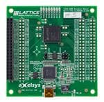
Figure 1 shows the top side of the iCE40HX-8K Evaluation Board indicating the specific features that are designed
on the board.
2
�iCE40HX-8K Breakout Board
Figure 1. iCE40HX-8K Evaluation Board (Top Side)
LEDs
iCE40HX-8K
0.1" spaced holes
40 pin header
USB
Figure 2. Block Diagram
HEADER
I/Os
LEDS(1-8)
USB
CONNECTOR
USB to
SPI / RS232
iCE40HX8K-CT256
RS232
Power from USB 5V
BANK 2
I/Os
HEADER
3
SPI
I/Os
HEADER
FPGA
BANK 1
I/Os
BANK 3
HEADER
BANK 0
�iCE40HX-8K Breakout Board
iCE40 Device
This board features an iCE40HX-8K device with a 1.2v core supply. It is packaged in a 256 caBGA package. For a
complete description of this device, see HB1011, iCE40 LP/LX/LM Family Handbook.
Software Requirements
You should install the following software before you begin developing designs for the evaluation board:
• Lattice iCEcube2 Release: 2012.09SP1.22498 or later
• Diamond Programmer: Version 2.2 or later
These software are available at the Lattice website Design Software & IP page. Make sure you log in to the Lattice
website, otherwise these software downloads will not be visible.
Demonstration Design
The design file iCE40HX8KLED.zip contains the following files:
• LED_VHDL.vhd (VHDL code)
• LED_Verilog.v
(Verilog code)
• LED.pcf (pin constraint file)
• LED_VHDL_bitmap.hex (Bit stream file for programming FPGA.)
• LED_Verilog_bitmap.hex (Bit stream file for programming FPGA.)
Two source codes are provided, one written in VHDL and the other in Verilog. Both of these codes function identically. This provides you with an option to use either one of the code when programming the Breakout Board. When
the FPGA is programmed with one of these codes, the red LEDs (D2 thru D9) will flash on for ½ second and off for
½ second.
Figure 3 shows the block diagram of the Verilog or VHDL code.
Figure 3. Block Diagram of the Verilog or VHDL Code
12MHz Clk
LED 2
LED 2
16
÷2
÷ 96
½ second pulse
2 bit counter
2
Decoder
LED 3
LED 9
The source code has two counters that are used to divide the 12MHz clock by 216 and 96 generating a approximately ½ second pulse. This pulse along with the decoder will turn the LEDs (D2 thru D9) on for ½ second and off
for ½ second. The decoder can be modified to have any type of LED sequence by changing either the VHDL or
Verilog code.
When the board is plugged into a USB port, a +5 volt power is applied to the board that will light a green LED
(D11). After the FPGA has been programmed, a green LED (D10) will light. This LED is connected to the CDONE
line of the FPGA.
4
�iCE40HX-8K Breakout Board
Board Power
The iCE40HX-8K evaluation board is powered with the USB cable. LED location D11 indicates that the board is
powered up. All I/Os are driven at 3.3v.
Board I/Os
The I/Os that feed the holes and the 0.1” connector are driven at 3.3v levels. Location J2 is the populated 2 x 20
row connector. Locations J1, J3 and J4 have hole locations that the users can connect to for their specific I/O
requirements.
Programming Options
Two jumpers, J6 and J7 can be set for two types of FPGA Configurations:
• SPI Flash Mode, for programming the serial flash memory.
• SPI Peripheral Mode, for configuring the volatile CRAM in the FPGA.
In SPI Flash Mode the SPI signals, from the FTDI USB interface chip, programs the serial flash memory. After the
memory is programmed the FPGA reads from the memory and configures its self. The advantage of programming
the serial flash is that the FPGA will be re-configured after power-up. Jumpers must be in locations J7:1-2, J6:2-4,
and J6:1-3. See Figure 4
Figure 4. SPI Flash Programming
In SPI Peripheral Mode the SPI signals loads the program file into the CRAM (configuration ram) of the FPGA
directly. In this mode the FPGA will lose its configuration when power is removed and must be re-configured. Jump5
�iCE40HX-8K Breakout Board
ers must be in locations J6:1-2 and J6:3-4. Jumper J7 is not installed. See Figure 5
Figure 5. CRAM Programming
LED in location D10 is connected to the CDONE pin of the iCE40HX-8K. This can be monitored to determine that
the iCE40HX-8K is programmed correctly.
Ordering Information
Description
Ordering Part Number
ICE40HX-8K Breakout Board
ICE40HX8K-B-EVN
6
China RoHS EnvironmentFriendly Use Period (EFUP)
�iCE40HX-8K Breakout Board
Technical Support Assistance
Submit a technical support case through www.latticesemi.com/techsupport.
Revision History
Date
Version
January 2016
1.1
Change Summary
Updated Technical Support AssistanceDemonstration Design section.
Changed “demonstration design” to “design file”.
Updated Technical Support AssistanceTechnical Support Assistance
section.
November 2013
1.0
Initial release.
© 2016 Lattice Semiconductor Corp. All Lattice trademarks, registered trademarks, patents, and disclaimers are as
listed at www.latticesemi.com/legal. All other brand or product names are trademarks or registered trademarks of
their respective holders. The specifications and information herein are subject to change without notice.
7
�8
A
B
C
D
5
USB
CONNECTOR
5
USB to
SPI / RS232
4
4
Power from USB 5V
3
RS232
I/Os
3
HEADER
2
I/Os
BANK 2
iCE40HX8K-CT256
FPGA
BANK 0
HEADER
I/Os
2
BANK 1
SPI
Date:
Size
B
Title
HEADER
Jul 11, 2013
ICE40HX8K-B-EVN
Document Number
1
Sheet
1
of
6
iCE40-HX8K Breakout Board - Block Diagram
AXELSYS
I/Os
LEDS(1-8)
1
Rev
A
A
B
C
D
iCE40HX-8K Breakout Board
Appendix A. Schematic Diagrams
Figure 6. Block Diagram
BANK 3
HEADER
�A
B
C
0.1uF
C12
+3.3V
8
7
6
5
CS
CLK
DI
DO
5
93LC56-SO8
VCC
NU
ORG
VSS
U2
1
2
3
4
10K
R8
10K
R9
0.1uF
0.1uF
0.1uF
0.1uF
+3.3V
C8
C7
C6
C5
+3.3V
10K
R10
R14
2.2K
0.1uF
C9
4
1
2
OUTPUT
VDD
12.0000MHZ
GND
STANDBY#
X1
3
4
0.1uF
10uF
+3.3V
C11
C10
VCC1_8FT
+3.3V
+3.3V
C1
0.1uF
C13
12K
2.2K
5
5
iCE_CLK
3
4
FT_EECS
FT_EECLK
FT_EEDATA
R11
R7
0.1uF
4.7uF
+3.3V
C4
R20
0
C2
0.1uF
C3
4.7uF
3
DM
DP
13
3
2
63
62
61
6
14
7
8
49
50
VCC1_8FT
FT2232H
+3.3V
PWREN#
BCBUS0
BCBUS1
BCBUS2
BCBUS3
BCBUS4
BCBUS5
BCBUS6
BCBUS7
BDBUS0
BDBUS1
BDBUS2
BDBUS3
BDBUS4
BDBUS5
BDBUS6
BDBUS7
ACBUS0
ACBUS1
ACBUS2
ACBUS3
ACBUS4
ACBUS5
ACBUS6
ACBUS7
ADBUS0
ADBUS1
ADBUS2
ADBUS3
ADBUS4
ADBUS5
ADBUS6
ADBUS7
SUSPEND#
FTDI High-Speed USB
TEST
OSCO
OSCI
EECS
EECLK
EEDATA
REF
RESET#
DM
DP
VREGOUT
VREGIN
U1
FT2232HL
AGND
10
D
4
4
9
VPHY
VPLL
12
37
64
VCORE
VCORE
VCORE
20
31
42
56
VCCIO
VCCIO
VCCIO
VCCIO
GND
GND
GND
GND
GND
GND
GND
GND
9
1
5
11
15
25
35
47
51
5
36
60
48
52
53
54
55
57
58
59
38
39
40
41
43
44
45
46
26
27
28
29
30
32
33
34
16
17
18
19
21
22
23
24
2
2
SS
SCK
SI
SO
0
0
0
0
0
0
0
0
0
0
0
0
0
Title
Date:
Size
B
AXELSYS
RS232_Rx_TTL
RS232_Tx_TTL
RTSn
CTSn
DTRn
DSRn
DCDn
iCE_CDONE
iCE_CREST
iCE_SS_B
iCE_SCK
FLASH_MOSI
FLASH_MISO
4
4
6
6
6
6
3
3
3
3
3
3
3
Jul 11, 2013
ICE40HX8K-B-EVN
Document Number
1
Sheet
2
of
6
Rev
A
iCE40-HX8K Breakout Board - USB to SPI/RS232
R12
R13
R15
R16
R17
R18
R19
R5
R6
R4
R1
R2
R3
1
A
B
C
D
iCE40HX-8K Breakout Board
Figure 7. USB to SPI/RS232
�10
A
B
C
D
1
5
R23
100
DNI
TP7
0.1uF
0.1uF
DNI
+1.2V TP6
C17
C14
1
R21
1
1
1
5
VCCIO0
0.1uF
10uF
PIO0_51
PIO0_47
PIO0_44
PIO0_34
PIO0_45
PIO0_46
PIO0_27
PIO0_30
PIO0_31
PIO0_15
PIO0_14
PIO0_20
PIO0_01
PIO0_03
C23
0.1uF
0.1uF
C22
C15
C18
0.1uF
VCCIO0
PIO0_00
PIO0_01
PIO0_02
PIO0_03
PIO0_04
PIO0_05
PIO0_06
PIO0_07
PIO0_08
PIO0_09
PIO0_10
PIO0_11
PIO0_12
PIO0_13
PIO0_14
PIO0_15
PIO0_16
PIO0_17
PIO0_18
PIO0_19
PIO0_20
PIO0_21
PIO0_22
PIO0_23
PIO0_24
PIO0_27
PIO0_28
PIO0_29
PIO0_30
PIO0_31
PIO0_32
PIO0_33
PIO0_34
PIO0_35
PIO0_36
PIO0_37
PIO0_38
PIO0_39
PIO0_40
PIO0_41
PIO0_42
PIO0_43
PIO0_44
PIO0_45
PIO0_46
PIO0_47
PIO0_48
PIO0_49
PIO0_50
PIO0_51
C14
B15
D13
B14
C12
E11
C13
A16
A15
B13
E10
C11
D11
B12
B10
B11
C10
A10
A11
D10
C9
E9
D9
A9
F9
B9
D8
B8
A7
C7
B7
B6
C6
D7
A6
D6
A5
B5
E6
B4
A2
D5
A1
C5
C4
B3
D4
E5
D3
C3
2
4
6
8
10
12
14
16
18
20
22
24
26
28
30
32
34
36
38
40
1
3
5
7
9
11
13
15
17
19
21
23
25
27
29
31
33
35
37
39
4
Header2x20
DNI
J1
MAKE PWR TRACES
CAPABLE OF 1A
GBIN0/PIO0_26
GBIN1/PIO0_25
BANK0
PLLVCC0
PLLGND_0
VCCIO0_01
VCCIO0_02
VCCIO0_03
VCCIO0_04
U3A
iCE40HX8K-CT256
C25
F7
C8
E8
E7
A13
A3
A8
F8
4
PIO0_39
PIO0_41
PIO0_42
PIO0_36
PIO0_33
PIO0_38
PIO0_23
PIO0_29
PIO0_32
PIO0_13
PIO0_18
PIO0_17
PIO0_07
PIO0_08
PIO0_09
PIO0_51
PIO0_44
PIO0_45
PIO0_46
PIO0_47
PIO0_41
PIO0_42
PIO0_38
PIO0_39
PIO0_36
PIO0_29
PIO0_30
PIO0_31
PIO0_32
PIO0_33
PIO0_34
PIO0_27
PIO0_23
PIO0_20
PIO0_17
PIO0_18
PIO0_13
PIO0_14
PIO0_15
PIO0_07
PIO0_08
PIO0_09
PIO0_03
PIO0_01
LED7
LED3
LED4
LED5
LED6
LED1
LED2
LED0
5
5
5
5
5
5
5
5
RS232_Tx_TTL
RS232_Rx_TTL
DTRn
CTSn
RTSn
DSRn
DCDn
3
3
2
2
2
2
2
2
2
PIO1_44
PIO1_51
PIO1_49
PIO1_32
PIO1_36
PIO1_46
PIO1_22
PIO1_42
PIO1_29
PIO1_14
PIO1_16
PIO1_21
PIO1_01
PIO1_03
DNI
+3.3V TP8
0.1uF
C24
1
R22
DNI
TP9
2
4
6
8
10
12
14
16
18
20
22
24
26
28
30
32
34
36
38
40
1
3
5
7
9
11
13
15
17
19
21
23
25
27
29
31
33
35
37
39
Header2x20
J2
2
0.1uF
C27
PIO1_38
PIO1_40
PIO1_47
GBIN2/PIO1_28
PIO1_30
PIO1_34
PIO1_18
PIO1_37
PIO1_19
PIO1_08
PIO1_12
PIO1_20
2
10K
R24
Date:
Size
B
Title
0.1uF
C20
GBIN2/PIO1_28
PIO1_03
PIO1_01
0.1uF
C16
PIO1_04
0.1uF
C26
0.1uF
C19
VCC_1.2V
0.1uF
C21
VCCIO1
MAKE PWR TRACES
CAPABLE OF 1A
VCCIO1
1
DNI
TP5
1
DNI
+3.3V TP4
PIO1_04
PIO1_05
PIO1_06
PIO1_07
PIO1_08
PIO1_09
PIO1_10
PIO1_11
PIO1_12
PIO1_13
PIO1_14
PIO1_15
PIO1_16
PIO1_17
PIO1_18
PIO1_19
PIO1_20
PIO1_21
PIO1_22
PIO1_23
PIO1_24
PIO1_25
PIO1_26
PIO1_29
PIO1_30
PIO1_31
PIO1_32
PIO1_33
PIO1_34
PIO1_35
PIO1_36
PIO1_37
PIO1_38
PIO1_39
PIO1_40
PIO1_41
PIO1_42
PIO1_43
PIO1_44
PIO1_45
PIO1_46
PIO1_47
PIO1_48
PIO1_49
PIO1_50
PIO1_51
P16
M13
M14
L12
N16
L13
L14
K12
M16
J10
M15
J11
L16
K13
K14
J15
K15
K16
J14
J12
J13
J16
H13
H14
G16
H12
G15
G10
F16
G11
F15
G14
E16
G13
D16
G12
F14
F12
D15
F11
E14
C16
F13
B16
E13
D14
PIO1_51
PIO1_49
PIO1_46
PIO1_47
PIO1_44
PIO1_42
PIO1_40
PIO1_36
PIO1_37
PIO1_38
PIO1_34
PIO1_32
PIO1_29
PIO1_30
PIO1_18
PIO1_19
PIO1_20
PIO1_21
PIO1_22
PIO1_16
PIO1_14
PIO1_12
PIO1_08
PIO1_04
Jul 27, 2013
ICE40HX8K-B-EVN
1
Sheet
3
of
iCE40-HX8K Breakout Board - FPGA
AXELSYS
GBIN2/PIO1_28
GBIN3/PIO1_27
BANK1
PIO1_00
PIO1_01
PIO1_02
PIO1_03
TRST_B
VCCIO1_01
VCCIO1_02
VCCIO1_03
VCCIO1_04
U3B
iCE40HX8K-CT256
Document Number
H16
H11
R14
R15
P14
P15
N14
H10
C15
H15
N15
1
6
Rev
A
A
B
C
D
iCE40HX-8K Breakout Board
Figure 8. FPGA
�11
A
B
C
2
1
iCE_CDONE
2
0.1uF
C38
5
PIO2_10
PIO2_09
PIO2_05
PIO2_21
PIO2_16
PIO2_08
PIO2_29
PIO2_28
GBIN5/PIO2_26
VCCIO2
R29
DNI
TP16
PIO2_45/CBSEL1
0.1uF
GBIN5/PIO2_26
2
4
6
8
10
12
14
16
18
20
22
24
26
28
30
32
34
36
38
40
1
3
5
7
9
11
13
15
17
19
21
23
25
27
29
31
33
35
37
39
Header2x20
DNI
J3
MAKE PWR TRACES
CAPABLE OF 1A
10K
10uF
C37
0.1uF
0.1uF
0.1uF
C36
C35
C34
C33
DNI
TP13
0.1uF
C32
iCE_CREST
PIO2_45/CBSEL1
PIO2_37
PIO2_31
PIO2_41
PIO2_36
D10
Green
649
R28
VCCIO2
R26
100
+3.3V
DNI
+1.2V TP12
1
1
D
1
R27
1
2
1
K9
R9
M10
N11
K11
P13
N8
L8
K8
P3
R13
R8
PIO2_07
PIO2_03
PIO2_01
PIO2_20
PIO2_18
PIO2_15
PIO2_33
PIO2_17
PIO2_24
PIO2_39
PIO2_32
PIO2_34
PIO2_43
PIO2_35
PIO2_38
4
GBIN4/PIO2_27
GBIN5/PIO2_26
CDONE
CRESET_B
PIO2_44/CBSEL0
PIO2_45/CBSEL1
BANK2
PLLGND_2
PLLVCC2
VCCIO2_01
VCCIO2_02
VCCIO2_03
VCCIO2_04
U3C
iCE40HX8K-CT256
4
PIO2_00
PIO2_01
PIO2_02
PIO2_03
PIO2_04
PIO2_05
PIO2_06
PIO2_07
PIO2_08
PIO2_09
PIO2_10
PIO2_11
PIO2_12
PIO2_13
PIO2_14
PIO2_15
PIO2_16
PIO2_17
PIO2_18
PIO2_19
PIO2_20
PIO2_21
PIO2_22
PIO2_23
PIO2_24
PIO2_25
PIO2_28
PIO2_29
PIO2_30
PIO2_31
PIO2_32
PIO2_33
PIO2_34
PIO2_35
PIO2_36
PIO2_37
PIO2_38
PIO2_39
PIO2_40
PIO2_41
PIO2_42
PIO2_43
N6
T1
P4
R2
N5
T2
P5
R3
R5
T3
R4
M7
N7
P6
M8
T5
R6
P8
T6
L9
T7
T8
P7
N9
T9
M9
P9
R10
L10
P10
N10
T10
T11
T15
T14
M11
T13
N12
L11
T16
M12
R16
PIO2_43
PIO2_41
PIO2_31
PIO2_32
PIO2_33
PIO2_34
PIO2_35
PIO2_36
PIO2_37
PIO2_38
PIO2_39
PIO2_28
PIO2_29
PIO2_24
PIO2_20
PIO2_21
PIO2_15
PIO2_16
PIO2_17
PIO2_18
PIO2_07
PIO2_08
PIO2_09
PIO2_10
PIO2_05
PIO2_03
PIO2_01
1
R25
3
3
PIO3_07/DP03B
PIO3_05/DP02B
PIO3_01/DP00B
PIO3_27/DP13B
GBIN7/PIO3_25/DP12B
PIO3_19/DP09B
PIO3_30/DP15A
PIO3_29/DP14B
GBIN6/PIO3_26/DP13A
PIO3_41/DP20B
PIO3_35/DP17B
PIO3_33/DP16B
0.1uF
C39
iCE_CLK
0.1uF
C30
2
4
6
8
10
12
14
16
18
20
22
24
26
28
30
32
34
36
38
40
1
3
5
7
9
11
13
15
17
19
21
23
25
27
29
31
33
35
37
39
Header2x20
DNI
J4
MAKE PWR TRACES
CAPABLE OF 1A
VCCIO3
2
0.1uF
C29
DNI
TP15 VCCIO3
PIO3_50/DP25A
PIO3_48/DP24A
DNI
+3.3V TP14
1
DNI
TP11 VCCIO2
1
5
1
DNI
+3.3V TP10
0.1uF
C28
VCC_3.3V
PIO3_09/DP04B
PIO3_04/DP02A
PIO3_03/DP01B
PIO3_21/DP10B
PIO3_17/DP08B
PIO3_13/DP06B
PIO3_31/DP15B
PIO3_28/DP14A
PIO3_23/DP11B
PIO3_45/DP22B
PIO3_39/DP19B
PIO3_37/DP18B
2
Date:
Size
B
Title
GBIN7/PIO3_25/DP12B
GBIN6/PIO3_26/DP13A
BANK3
VCCIO3_01
VCCIO3_02
VCCIO3_03
VCCIO3_04
U3D
iCE40HX8K-CT256
0.1uF
C41
PIO3_46/DP23A
0.1uF
C40
GBIN7/PIO3_25/DP12B G1
GBIN6/PIO3_26/DP13A J3
0.1uF
C31
E1
G6
J6
N1
2
J2
J1
K1
K3
L4
L1
K4
M1
L6
L3
K5
M2
L7
N2
M6
M3
L5
N3
P1
M4
P2
M5
R1
N4
H1
J5
E4
B2
F5
B1
C1
C2
F4
D2
G5
D1
G4
E3
H5
E2
G3
F3
H3
F2
H6
F1
H4
G2
J4
H2
PIO3_01/DP00B
PIO3_50/DP25A
PIO3_48/DP24A
PIO3_45/DP22B
PIO3_46/DP23A
PIO3_41/DP20B
PIO3_39/DP19B
PIO3_37/DP18B
PIO3_35/DP17B
PIO3_33/DP16B
PIO3_28/DP14A
PIO3_29/DP14B
PIO3_30/DP15A
PIO3_31/DP15B
PIO3_27/DP13B
PIO3_23/DP11B
PIO3_21/DP10B
PIO3_19/DP09B
PIO3_17/DP08B
PIO3_13/DP06B
PIO3_09/DP04B
PIO3_07/DP03B
PIO3_03/DP01B
PIO3_04/DP02A
PIO3_05/DP02B
Jul 26, 2013
ICE40HX8K-B-EVN
Document Number
1
Sheet
4
of
iCE40-HX8K Breakout Board - FPGA
AXELSYS
PIO3_28/DP14A
PIO3_29/DP14B
PIO3_30/DP15A
PIO3_31/DP15B
PIO3_32/DP16A
PIO3_33/DP16B
PIO3_34/DP17A
PIO3_35/DP17B
PIO3_36/DP18A
PIO3_37/DP18B
PIO3_38/DP19A
PIO3_39/DP19B
PIO3_40/DP20A
PIO3_41/DP20B
PIO3_42/DP21A
PIO3_43/DP21B
PIO3_44/DP22A
PIO3_45/DP22B
PIO3_46/DP23A
PIO3_47/DP23B
PIO3_48/DP24A
PIO3_49/DP24B
PIO3_50/DP25A
PIO3_51/DP25B
PIO3_27/DP13B
PIO3_24/DP12A
PIO3_00/DP00A
PIO3_01/DP00B
PIO3_02/DP01A
PIO3_03/DP01B
PIO3_04/DP02A
PIO3_05/DP02B
PIO3_06/DP03A
PIO3_07/DP03B
PIO3_08/DP04A
PIO3_09/DP04B
PIO3_10/DP05A
PIO3_11/DP05B
PIO3_12/DP06A
PIO3_13/DP06B
PIO3_14/DP07A
PIO3_15/DP07B
PIO3_16/DP08A
PIO3_17/DP08B
PIO3_18/DP09A
PIO3_19/DP09B
PIO3_20/DP10A
PIO3_21/DP10B
PIO3_22/DP11A
PIO3_23/DP11B
1
6
Rev
A
A
B
C
D
iCE40HX-8K Breakout Board
Figure 9. FPGA
�A
B
C
D
VCC
DD+
ID
GND
1
2
3
4
5
5
SKT_MINIUSB_B_RA
J5
1M
1M
10uF
0
0.1uF
R48
C62
600 Ohm 500 mA
L3
VBUS_5V
R35
R34
C54
VBUS_5V
0.1uF
C61
21
12
19
11
20
18
17
14
13
1uF
10uF
DM
DP
1K
R53
THERMPAD
PWRGD2
PWRGD1
SHDN2
SHDN1
IN1_1
IN1_2
IN2_1
IN2_2
U4
0.1uF
GND1
2
2
16
GND2
15
1
2
D11
Green
10
9
8
7
1
2
4
3
0.1uF
C46
0.01uF
C59
0.01uF
C55
0.1uF
C47
4
LT3030EFE#TRPBF
ADJ2
BYP2
OUT2_2
OUT2_1
ADJ1
BYP1
OUT1_2
OUT1_1
0.1uF
C45
GND3
5
GND4
6
C44
357K
R32
4.7uF
C58
210K
A12
A4
E15
G7
G8
G9
H7
H8
H9
J7
J8
J9
K2
K7
L15
R7
T12
T4
0.1
R37
10uF
C53
0.1
R31
GND_01 VPP_FAST
GND_02
VPP_2V5
GND_03
GND_04
GND_05
GND_06
GND_07
GND_08 POWER
GND_09
GND_10
GND_11
GND_12
GND_13
VCC_01
GND_14
VCC_02
VCC_03
GND_15
GND_16
VCC_04
GND_17
VCC_05
VCC_06
GND_18
L2
22uF
C56
VCC_3.3V
A14
F10
F6
K10
K6
L2
D12
E12
3
D1
C57
1
1
R38
+1.2V
L1
+1.2V
600 Ohm 500 mA
+3.3V
0.1uF
CDBU0520
2
600 Ohm 500 mA
22uF
C60
VCC_1.2V
100
R33
+3.31V
U3F
iCE40HX8K-CT256
100
R39
+1.22V
R36
0.01uF
C48
LED5
LED7
3
LED4
LED6
LED3
3
3
LED2
3
3
LED1
3
LED0
3
3
+3.3V
2
+3.3V
C49
R40
D2
Red
1K
C52
Date:
Size
B
Title
D3
Red
1K
R42
R43
D5
Red
1K
D6
Red
1K
R44
D7
Red
1K
R45
1
D8
Red
1K
R46
1
Jul 26, 2013
ICE40HX8K-B-EVN
Document Number
1
Sheet
5
of
6
D9
Red
1K
R47
iCE40-HX8K Breakout Board - Power, LEDs
AXELSYS
D4
Red
1K
LEDs
DNI
TP3
DNI
TP2
0.01uF
DNI
R41
1uF
+1.2V
C51
0.1uF
C50
+3.3V
TP1
10uF
1
C43
1
2
C42
1
2
+1.2V
2
2
1
2
1
1
1
1
2
3
1
2
4
1
2
12
2
5
Rev
A
A
B
C
D
iCE40HX-8K Breakout Board
Figure 10. Power and LEDs
�13
A
B
C
5
JU2
63429-202LF
JU1
63429-202LF
JU3
63429-202LF
Short-circuit Jumper
N13
4
0.1uF
C63
+3.3V
4
SPI
SPI_VCC
2
iCE_SS_B
2
P12
P11
R11
R12
1
J7
iCE_MISO
iCE_MOSI
2
1
3
6
5
CS
WP
SCK
SDI
U5
10K
R49
C64
7
2
FLASH_MISO
N25Q032A13ESC40F
HOLD
SDO
0.1uF
R52
10K
R51
10K
R50
10K
2
iCE_MOSI
FLASH_MOSI
2
4
FLASH_MISO
iCE_MISO
2
3
For programming iCE - Shunt 3,4 and 1,2
2
For programming Flash - Shunt 1,3 and 2,4 (default)
1
3
J6
J7: Remove shunt only for Programming iCE.
Replace shunt for programming Flash and for normal operation.
iCE_SCK
2
FLASH_MOSI
PIOS_00/SPI_SO
PIOS_01/SPI_SI
PIOS_02/SPI_SCK
PIOS_03/SPI_SS_B
U3E
iCE40HX8K-CT256
3
8
VCC
GND
4
D
5
Date:
Size
B
Title
AXELSYS
Jul 26, 2013
ICE40HX8K-B-EVN
Document Number
1
Sheet
iCE40-HX8K Breakout Board - SPI
1
6
of
6
Rev
A
A
B
C
D
iCE40HX-8K Breakout Board
Figure 11. SPI
�
很抱歉,暂时无法提供与“ICE40HX8K-B-EVN”相匹配的价格&库存,您可以联系我们找货
免费人工找货- 国内价格 香港价格
- 1+1114.007511+144.19666