USB Type-C Demo Kit V2 Board User Guide
EB99 Version 1.0, June 2015
�USB Type-C Demo Kit V2 Board
Introduction
The USB Type-C Demo Kit V2 has been developed to support a variety of demos, encompassing different levels of
the USB Type-C functionality which includes Power Delivery and negotiation, power and data role swap, control channel negotiation, super speed signaling, DP alternate mode support and a low speed signal aggregation function.
There are two versions of this board, as identified by the Ordering Part Numbers (iCE40LP8K-USBC-EVN and
iCE5LP4K-USBC-EVN). This document is applicable to either version, with the notes as applicable.
The main circuits on the development kit board:
• Programming Circuit
— Mini-USB Type B connector to FTDI
— FTDI to MachXO2™ Programming Mux
• MachXO2-4000ZE
— Programming Multiplexing
— Signal Generator and Receiver for aggregation
— General Purpose I/O
— LED Display Control
• iCE40LP-8K (iCE40LP8K-USBC-EVN only)
— Super-speed signaling control
— CD-PD physical layer and power delivery manager
— Billboard support
— DP alternate mode support and control
— Aggregator support
— AP interface
— Data logging
• iCE5LP-4K (iCE5LP4K-USBC-EVN only)
— Super-Speed signaling Control
— CD-PD physical layer and power delivery manager
— AP interface
— Data logging
2
�USB Type-C Demo Kit V2 Board
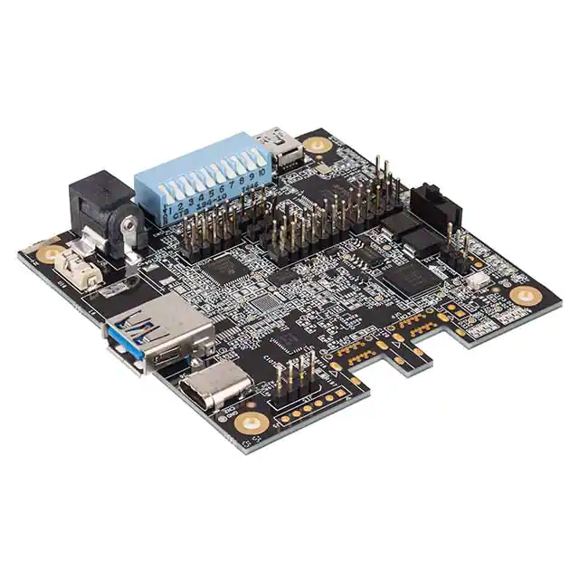
Figure 1 is the top view of the USB Type-C Demo Kit V2 Board showing the key components present on the board.
Figure 1. Top View of USB Type-C Demo Kit V2 Board with Key Components
Power Switch (SW2)
LEDs (D17-D25)
LEDs (D1-D8)
FTDI Chip (U1)
LEDs (D26-D33)
USB 2.0 Mini-B (J2)
LCMXO2-4000ZE (U4)
DP Connector UFP (CN1)2
10-Bit Switch (SW3)
DP Connector DFP (CN2)2
Header Pool
iCE40LP8K (U22)2
HD3SS460 (U11)
P13D6S3224 (U19)
Power Jacket (J8)
SN8F22511BX (U13)2
Boost
Regulator
(U18)
USB Type-C Receptacle (CN2)
iCE5LP4K (U5)1
Notes:
1. iCE5LP4K-USBC ENV Only
2. iCE40LP8K-USBC ENV Only
USB Type-A Receptacle (J6)
3
�USB Type-C Demo Kit V2 Board
Headers and Test Connectors
Figure 2 shows the top view of the demo board. The numbers of headers and test connectors which provide
access to USB Type-C Demo Kit V2 Board circuits are indicated.
Figure 2. Top View of the USB Type-C Demo Kit V2 Board with Headers and Test Connectors
J1 J3
J7 J20
SW2
J12
J10
SW1
J17
(SW3)
J5
J15
J18 J16 J9 J19
Table 1 provides the detailed definition of the headers and test connectors.
Table 1. Headers and Test Connectors
Part
Description
Setting Options
Default Setting
J1
External JTAG I/F
J3
JTAG/SPI Selection
1-2 (SPI), 2-3 (JTAG)
JTAG
J16
JTAG/I2C Selection
1-2 (JTAG), 2-3 (I2C)
JTAG
SW1
MachXO2 Reset Switch
J17
Jumper for DP Power
Open-Off, Short-On
Open
J5
BB Device Programmer I/F
SW2
Board Power Switch
Left-On, Right-Off
Right
J7
VBUS Sink Connector
Open-Off, Short-On
Open
SW3
General Purpose Input Switch
J9
USB Role Selection
1-2 (UFP), 2-3 (DFP)
Open
J10
MachXO2 I/O HIZ Enable
1-2 (Enable), 2-3 (Disable)
Open
J15
For Testing/Probing
J12
MachXO2 I/O Direction Input
1-2 (Input), 2-3 (Output)
Open
J20
For Testing/Probing
J18
External I2C I/F
J19
External AGG Inputs
4
�USB Type-C Demo Kit V2 Board
Programming Circuit
The Mini-USB Type B connector is used for programming the board, using the standard Diamond Programmer software. Figure 3 shows the programming block of the USB Type-C Demo Kit V2.
The Mini-USB Type B connector interfaces with the FTDI FT2232H IC. The FTDI IC works with Diamond programmer to provide interfaces for JTAG (for programming MachXO2-4000ZE) and SPI (for programming both the
iCE40™ LP and iCE40 Ultra™ devices and their SPI Flash Memories). The SPI programming works in conjunction
with a mux design that must be programmed into the MachXO2-4000ZE. The mux design operation and required
switch settings are described in detail in the next section. When the MachXO2 device contains the mux design and
the proper switch settings are chosen, the Diamond Programmer interfaces directly with the iCE40 devices or SPI
Flashes.
Figure 3. Programming Block
J2
U1
U4
USB MINI-B
FTDI
FT2232H
LCMX0240002E
SW3
Switch
U5/U22
ICE40LP8KCM81 or
ICE5LP4K-48
U10
FLASH
Programming Mux and Switch Settings
The board allows for programming the various devices contained on the USB Type-C Demo Kit V2:
• MachXO2 (LCMXO2-4000ZE-1MG132C) – U4
• iCE40 LP (iCE40LP8K-CM81) – U22
— Configuration or Programming
— iCE40 Ultra External SPI Flash – U10
— Micron Technology Inc. (N25Q032A13ESC40F)
— CDONE LED (Red) – D11
• iCE40 Ultra (iCE5LP4K-SG48) – U7
— Configuration or Programming
— iCE40 Ultra External SPI Flash - U6
— Micron Technology Inc (N25Q032A13ESC40F)
— CDONE LED (Green) – D9
• iCE40 Device CRESETB can be asserted by pushing SW1
— Routed through MachXO2 device
5
�USB Type-C Demo Kit V2 Board
Figure 4 shows the DIP switch numbering and settings.
Figure 4. DIP Switch Numbering
SW3.1
SW3.2
SW3.3
SW3.4
J16
SW3.5
(SW3)
SW3.6
SW3.7
J3
SW3.8
SW3.9
SW3.10
Two positions of the DIP switch SW3 and the header J3 are used to control which devices and which mode the
FTDI Bridge utilizes. Table 2 provides the detailed definitions of the DIP switch settings required to program each
device.
Table 2. DIP Switch Settings to Program the Device
Device
Jumper Position
DIPSW (SW3) Position
Operation
Mode
J16
J3
SW3.10
SW3.9
MachXO2
Program/Configure
JTAG
1-2
3-2
Up
Down
iCE40 CRAM
Program/Configure
SPI
1-2
1-2
Down
Down
iCE40 Flash
Program/Configure
SPI
1-2
1-2
Down
Up
(All)
Boot
—
3-2
—
Up
Up
Note: The MachXO2 must be programmed with an image containing the SPI programming multiplexing and CRESET
level-shifting driver (for example, the default image asdf.jed) prior to programming or configuring the iCE40 devices or
their subtended SPI Flash devices.
6
�USB Type-C Demo Kit V2 Board
Status Indicators
The board provides the number of LED status indicators, shows power, configuration, and an application status.
Table 3 provides the detailed definition of the Status LED I/O Map.
Table 3. Status LED I/O Map
Device
LCMX02-4000ZE
I/O Balls
LED
B1
D1
Schematic NET
AGG_LED1
Bank
3
Color
Green
LCMX02-4000ZE
B2
D2
AGG_LED2
3
Green
LCMX02-4000ZE
C1
D3
AGG_LED3
3
Green
LCMX02-4000ZE
C2
D4
AGG_LED4
3
Green
LCMX02-4000ZE
C3
D5
AGG_LED5
3
Green
LCMX02-4000ZE
D1
D6
AGG_LED6
3
Green
LCMX02-4000ZE
E1
D7
AGG_LED7
3
Green
LCMX02-4000ZE
E2
D8
AGG_LED8
3
Green
LCMX02-4000ZE
J3
D17
STATUS_LED1
3
Blue
LCMX02-4000ZE
K1
D20
STATUS_LED2
3
Blue
LCMX02-4000ZE
K2
D22
STATUS_LED3
3
Green
LCMX02-4000ZE
K3
D23
STATUS_LED4
3
Green
LCMX02-4000ZE
L3
D26
STATUS_LED5
3
Red
LCMX02-4000ZE
M1
D27
STATUS_LED6
3
Red
LCMX02-4000ZE
M2
D30
STATUS_LED7
3
Yellow
LCMX02-4000ZE
N9
D31
STATUS_LED8
2
Yellow
LCMX02-4000ZE
N10
D33
STATUS_LED9
2
Yellow
LCMX02-4000ZE
P2
D18
STATUS_LED10
2
Blue
LCMX02-4000ZE
P4
D19
STATUS_LED11
2
Blue
LCMX02-4000ZE
P6
D21
STATUS_LED12
2
Green
LCMX02-4000ZE
P7
D23
STATUS_LED13
2
Green
LCMX02-4000ZE
P8
D25
STATUS_LED14
2
Green
LCMX02-4000ZE
P9
D28
STATUS_LED15
2
Blue
LCMX02-4000ZE
P11
D29
STATUS_LED16
2
Blue
LCMX02-4000ZE
P12
D32
STATUS_LED17
2
Blue
ICE5LP4K
7
D9
4KDONE
2
Red
ICE40LP8K
E6
D11
CDONE
2
Red
7
�USB Type-C Demo Kit V2 Board
MachXO2-4000ZE Circuit Overview
LCMXO2-4000ZE-1MG132C
The MachXO2 device (LCMXO2-4000ZE-1MG132C) on the board performs a variety of functions:
• Programming Multiplexing
— Interface from PC/FTDI to iCE5LP, iCE40LP, and SPI Flash memories
• Signal Aggregator Demo Function
— Includes interface to iCE40LP8K
• General Purpose I/O from DIP switches and LEDs
The USB demo design includes bitstreams for the MachXO2.
Note: Refer to the documents accompanying each demo for details on the specific design function of the
MachXO2.
Tables provide the detailed definition of the different functions:
• LED Indication (Table 3)
• Switches (Table 4)
— DIP Switches
— Push Button
— 3-pin Headers
• iCE40LP8K/iCE5LP4K Interface (Table 5)
• External Application Processor Interface (Table 6)
Table 4 provides the detailed definition of the I/O Map for the device MachXO2 general purpose functions.
Table 4. Switches / I/O Map for MachXO2
Device
I/O Ball
Schematic Net
Bank
Designator
LCMX02-4000ZE
B9/B12
CONFIG_SW1
0
SW3
LCMX02-4000ZE
B14
CONFIG_SW2
1
SW3
LCMX02-4000ZE
C13
CONFIG_SW3
1
SW3
LCMX02-4000ZE
C14
SW4
1
SW3
LCMX02-4000ZE
D12
SW5
1
SW3
LCMX02-4000ZE
E12
SW6
1
SW3
LCMX02-4000ZE
E13
SW7
1
SW3
LCMX02-4000ZE
E14
SW8
1
SW3
LCMX02-4000ZE
F12
SW9
1
SW3
LCMX02-4000ZE
F13
SW10
1
SW3
LCMX02-4000ZE
A2
XO2_RESET
0
SW1
POWER
—
5V
—
SW2
8
�USB Type-C Demo Kit V2 Board
Table 5. Aggregator I/O Map for MachX02
MACHX02(U4)
ICE40LP8K(U22)
I/O Ball
Bank
I/O Ball
Bank
HD3SS460(U11)
Pin Number
F1
3
B6
0
—
AGG_GPIO1
F2
3
A6
0
—
AGG_GPIO2
F3
3
B5
0
—
AGG_GPIO3
G3
3
A4
0
—
AGG_GPIO4
H1
3
B4
0
—
AGG_GPIO5
H2
3
D5
0
—
AGG_GPIO6
H3
3
E5
0
—
AGG_GPIO7
Schematic Net
J1
3
A3
0
—
AGG_GPIO8
B8
0
A8
0
—
SDA1
C8
0
B8
0
—
SCL1
A9
0
B7
0
—
SDA2
A7
0
A7
0
—
SCL2
A2
0
13
AUX_CHP
A1
0
14
AUX_CHN
The MachXO2-4000ZE and an iCE40LP8k/iCE5LP4K provides connections to the header J18 (Embedded controller connector). Table 6 provides the detailed definition of the signals.
Table 6. AP Interface for MachXO2, iCE40LP/iCE5LP and J18
iCE40LP8K(U22)
iCE5LP4K(U5)
XO2(U4)
J18
Schematic Net
Name
IO Ball
Bank
IO Ball
Bank
IO Ball
Bank
G7
SPI
15
2
M7
2
1
SPI_SCK
G4
2
18
2
N4
2
3
EC_CS
G6
SPI
14
2
M9
2
5
SPI_MISO
H7
SPI
17
2
M8
2
8
SPI_MOSI
9
�USB Type-C Demo Kit V2 Board
iCE40LP8K
The iCE40LP8K (U5/U22) is one of the devices on the board used to demonstrate the Lattice Type-C Power Delivery (PD) management and Cable Detect (CD) solution. In order to support the variety of demos, the iCE device
provides multiple parallel and serial connections to the MachXO2 device on the board. Table 5 and Table 6 provide
the detailed definition of the connections. Both the devices are connected to the J18 (Embedded Controller
header).
The iCE configuration may be stored in external SPI Flash (Refer the section Programming Mux and Switch Settings for more information. The external SPI Flash (U10) is connected to the configuration SPI port of the iCE
device. These signals, along with the CDONE and CRESET signals from the iCE are connected to the MachXO24000ZE device to facilitate connection from the PC (for programming) to both the iCE and SPI Flash.
The 25 MHz oscillator X2 is used to provide an external clock signal to the iCE40LP device. This clock signal is
also passed to the iCE5LP device. Table 7 provides the detailed definition of the clock connections.
Table 7. Clock Connections for iCE40LP
ICE40LP8K(U22)
ICE5LP4K(U5)
Schematic Net
IO Ball
Bank
IO Ball
Bank
Name
D8
1
20
2
CLK IN
Power Supply
Power supply to the development kit is by the MINI-USB Type-B connector or from an external adaptor. This connector provides 5 V source for the voltage regulators on the board which supply the power to MachXO2 and iCE
devices on the board. Each IO and core voltage rail on the board is accessible by a test point on the board. The
current flowing to each rail can also be measured using a 1Ω resistor placed in the path of each voltage rail.
Figure 5 shows the device power rails. There are three voltage regulators on the board used to supply the 3.3 V,
1.8 V, and 1.2 V rails. The input to these regulators is the 5 V rail on the board, which is supplied from either the
MINI-USB Type-B connector or external power adaptor via switch SW2.
Figure 5. Device Power Rails
J8
EXT
ADAPTER
U14
SW2
J2
LD0
VCC3V3
5V
U15
USB MINI
LD0
VCC1V2
U21
LD0
DP3V3
Several of the voltage rails also connect to indicator LEDs on the board to display the power status to the user.
These LEDs are listed in Table 8.
10
�USB Type-C Demo Kit V2 Board
Table 8. Voltage Rail Indicator LEDs
Voltage Rail
Indicator LED
Color
INT_5V
D12
Blue
VCC3V3
D14
Yellow
5V
D14
Yellow
The board voltage rails are summarized in Table 9, including the rail source voltage, test point #, and current sense
resistor number.
Table 9. Device Power Rail Summary and Test Points
Voltage Rail
VCC_SPI
Source Rail
VCC3V3
Sense Resistor
Test Point #
—
TP18
VCONN_5V
5V
R106
—
XO2_VCCIO0
VCC3V3
R107
TP6
XO2_VCCIO1
VCC3V3
R109
TP8
XO2_VCCIO2
VCC3V3
R111
TP10
XO2_VCCIO3
VCC3V3
R113
TP12
ICEVCCIO0
VCC3V3
R108
TP7
ICEVCCIO1
VCC3V3
R110
TP9
ICEVCCIO2
VCC3V3
R112
TP11
ICEVCCIO3
VCC3V3
R114
TP13
XO2_CORE
VCC3V3
R102
TP4
ICE4K_CORE
VCC3V3
R104
TP5
ICE8K_CORE
VCC3V3
R105
TP16
DP3V3
INT_5V
—
—
5V
USB5V/EXT_5V
—
TP17
VBUS
EXT_5V
—
—
11
�USB Type-C Demo Kit V2 Board
USB Super-Speed Switch/Alternate Mode Function
The development kit includes a super-speed switch IC (U11 - HD3SS460) along with a high-speed USB switch
(U19 – PI3DBS3224). The super-speed switch IC is used to demonstrate the orientation-agnostic capability of the
USB Type-C connector. The switches connect various USB sockets. Figure 6 shows the switch functions and the
data flow diagram.
Figure 6. Super Speed Block
T1
HD3SS460
(U12)
USB
Type B
(J4)
SSRX+/-
SSRX
CRX1
RX1
SSTX+/-
SSTX
CTX1
TX1
SS
LNA
LNB
LNC
DP
CRX2
RX2
CTX2
TX2
Type C
Connector
(CN1)
LNQ
RFU1
SBU1
RFU2
EN
POL
AMSEL
HS
SBU2
U11 is connected on one side to the standard-USB 9-pin connector (J6), the Mini DP connectors (CN1 and CN3)
and the other side connected to the USB Type-C connector (CN1). J6 provides a bi-directional Super-Speed channel as well as a bi-directional High-Speed channel, with CN1, CN2 providing a unidirectional display source data.
The U11 switch connection is managed by the iCE40 device on the board, using the SS_EN, SS_AMSEL, and
SS_POL signal inputs to U11. For more information refer the documentation on the super-speed switch demo.
Table 10 provides the detailed definition of the mode supported by the super speed switch.
12
�USB Type-C Demo Kit V2 Board
Table 10. Modes Supported by Super Speed Switch
POL
AMSEL
EN
Configurations
High Speed Signal Flow
SSRX
2CH USB SS
L
L
H
+ 2CH AM
(Normal)
2CH USBSS
H
L
H
+ 2CH AM
(Flipped)
LnD
CTX 1
LnC
CTX 2
LnB
CRX 2
LnA
H
H
4CH AM
(Normal)
LnD
CTX 1
LnC
CTX 2
LnB
CRX 2
LnA
H
H
H
4CH AM
(Flipped)
SBU 1
SBU 2
CSBU 1
SBU 1
CSBU 2
SBU 2
SSTX
CRX 1
LnD
CTX 1
LnC
CTX 2
LnB
CRX 2
LnA
SSRX
CSBU 1
CSBU 2
SSTX
CRX 1
SSRX
L
SSTX
CRX 1
SSRX
SBU Signal Flow
CSBU 1
SBU 1
CSBU 2
SBU 2
CSBU 1
SBU 1
CSBU 2
SBU 2
SSTX
CRX 1
LnD
CTX 1
LnC
CTX 2
LnB
CRX 2
LnA
Note: This board (iCE40LP8K-USBC-EVN) supports Display Port as an Alternate Mode function. By default board
population option is data sink. To modify it as data source, make the following changes on the board.
R199,R201,R203,R205,R207,R209,R211,R213,R215,R217-Do Not Populate
R198,R200,R202,R204,R206,R208,R210,R212,R214,R216-Populate
13
�USB Type-C Demo Kit V2 Board
USB High Speed Function
High speed switch function done by the device (U19) which receives inputs from the standard-USB 3.0 type A connector J6 and the Billboard device (U13) data using USB2.0 protocol and switches either of one to the Type-C connector (CN2). The switching behavior of U13 is controlled by the iCE device using the HS_SAI and HS_EN signals.
Figure 7 shows the High Speed Switch.
Figure 7. High Speed Switch
U19
CN2
HS Switch
TypeC
CONN
J6
USB CONN
U13
BB DEVICE
ICE5LP4K/ICE40LP8K
Table 11 provides the detailed definition of the MUX selection.
Table 11. MUX Selection
ENA/B
SAI
OUTA0
0
X
Hi-Z
1
1
INA
1
0
INB
14
�USB Type-C Demo Kit V2 Board
Billboard Interface
Billboard interface is the feature supported by USB Type-C protocol and which functioned by U13 and based on the
iCE control for the HS switch it will be terminated to the Type-C connector (CN2). Table 12 provides the detailed
definition of the Billboard Interface I/O map and associated net names.
Table 12. Billboard Interface
ICE40LP8K(U22)
I/O Ball
Bank
SNF225111BX(U13)
J5
PI3DBS3224(U19)
Pin Name
Pin Number
Pin Number
Schematic Net
C4
0
P5.0/SCK
—
—
BB_SCK
H5
2
P5.0/SDO
—
—
BB_SDO
G5
2
P5.1/SDI
—
—
BB_SDI
C5
0
P0.1/INT1
—
—
BB_INT
—
—
P1.0
2
—
BB_PGM
—
—
P1.1
3
—
BB_ALSB/PDB
—
—
P2.0
5
—
BB_CLK
—
—
P2.1
4
—
BB_OE
—
—
DN
—
4
BB_DN
—
—
DP
—
3
BB_DP
Data Logging Interface
Data logging interface can use a terminal screen such as HyperTerminal or Putty to display PD transactions of the
USB Type-C Demo Kit V2. Figure 8 shows the data flow and the block diagram of the data logging interface.
Figure 8. Data Logging Interface
U3
L22
MXU
ICE40LP8KCM81
U1
JTAG/I2C
J2
USB MINI-B
FTDI
FT2232HL
U4
U5
UART
LCMX0240002E
ICE5LP4K-48
Ordering Information
Description
Ordering Part Number
iCE40LP8K USB Type-C Demo Kit V2
iCE40LP8K-USBC-EVN
iCE40 Ultra USB Type-C Demo Kit V2
iCE5LP4K-USBC-EVN
15
China RoHS EnvironmentFriendly Use Period
�USB Type-C Demo Kit V2 Board
Technical Support Assistance
Submit a technical support case via www.latticesemi.com/techsupport.
Revision History
Date
Version
June 2015
1.0
Change Summary
Initial release.
© 2015 Lattice Semiconductor Corp. All Lattice trademarks, registered trademarks, patents, and disclaimers are as
listed at www.latticesemi.com/legal. All other brand or product names are trademarks or registered trademarks of
their respective holders. The specifications and information herein are subject to change without notice.
16
�17
A
B
C
D
USB-Mini-B
Connector
5
FT2232HL
FTDI
JTAG/SPI
I2C
N25Q032A13ESC40F
SPI Flash
SPI
I2C
SPI
I2C
2*I2C, 8GPIO
Headers
4
External
Power
Connector
3
ICE5LP4K-SG48
ICE40LP8K-CM81
USB3.1 Data(Tx,Rx)
Note:
1)Either ICE5LP4K or ICE40LP8K will be poplated not
Aardvark
Connector
Aggregator
LED's
LCMXO2-4000ZE
Status LED's
USB3.1-A-Female
Connector
Sink Mini DP
Connector
X4 DP Data Pairs
3
both
5V
CC Rx,Tx
CC Rx
Comparator
PI3DBS3224
SN8F22511BX
CC Tx
HS Switch
BB-USB PHY
Aggregator Data
ISL97656
2
HD3SS460
USB
SS/AM
SWITCH
Power-Reg
HS CNTRL
Source Mini DP
Connector
4
2
SS CNTRL
5
5V
20V
Date:
Size
B
24-FEB-2015
Type-C Connector
1
Sheet
Lattice Semiconductor Applications
Email: techsupport@Latticesemi.com
CC
Project
Lattice USB Type-C Evaluation Board
Title
BLOCK Diagram
Voltage
Selector
MOSFET's
CNTRL
VBUS(20V or 5V)
TS5A23159RSER
SPDT Switch
CC/VCONN SEL SWITCH
VCONN
USB2.0 D+/D-
DP AUX/Aggregator Data(SBU)
X4 DP/USBSS Data Pairs
1
Board Rev
o f 10
1
B
Schematic Rev 1.3
A
B
C
D
USB Type-C Demo Kit V2 Board
Appendix A. Schematic Diagrams
Figure 9. Block Diagram
�A
B
C
D
VCC
DD+
ID
GND
1
2
3
4
5
L2
0
0.1uF
C6
R3
600ohm 500mA
C1
0.1uF
CS
CLK
DI
DO
C15
0.1uF
10K
0.1uF
1
2
3
4
C14
5
93LC56-SO8
VCC
NU
ORG
VSS
U2
0.1uF
8
7
6
5
R15
C13
VCC3V3
0.1uF
C10
VCC3V3
VCC3V3
10K
R16
12k
0.1uF
C16
10K
R17
MINI USB FOR PROGRAMMING AND POWER
SKT_MINIUSB_B_RA
J2
1
2
0.1uF
C17
R18
4
VCC1V8FT
10uF
C7
VCC1V8FT
0.1uF
C18
0.1uF
C8
L3
C11
18pF
0.1uF
C19
1
2
600ohm 500mA
VCC3V3
L1
1
2
600ohm 500mA
VCC3V3
2
1
3
0.1uF
C20
12MHZ
4
3
VCC3V3
C4
4u7
C2
4u7
G1 G2
1
X1
1
2
1
2
USB5V
R14
2k2
DM
DP
C12
18pF
FT_EECS
FT_EECLK
FT_EEDATA
12k
R13
0.1uF
C5
0.1uF
C3
3
3
13
3
2
63
62
61
6
14
7
8
49
50
VCC1V8FT
FT2232H
FTDI High-Speed
TEST
OSCO
OSCI
EECS
EECLK
EEDATA
REF
RESET#
DM
DP
VREGOUT
VREGIN
U1
FT2232HL
AGND
VCC3V3
BDBUS0
BDBUS1
BDBUS2
BDBUS3
BDBUS4
BDBUS5
BDBUS6
BDBUS7
ACBUS0
ACBUS1
ACBUS2
ACBUS3
ACBUS4
ACBUS5
ACBUS6
ACBUS7
ADBUS0
ADBUS1
ADBUS2
ADBUS3
ADBUS4
ADBUS5
ADBUS6
ADBUS7
36
60
48
52
53
54
55
57
58
59
38
39
40
41
43
44
45
46
26
27
28
29
30
32
33
34
16
17
18
19
21
22
23
24
1
2
3
0
0
0
0
0
0
0
0
0
0
R232
R233
4.7k
R171
VCC3V3
2
2
Manual selection for I2C/JTAG
HEADER 3
J16
SUSPEND#
PWREN#
BCBUS0
BCBUS1
BCBUS2
BCBUS3
BCBUS4
BCBUS5
USB BCBUS6
BCBUS7
1-2 For JTAG
3-2 For I2C
10
4
4
9
VPHY
VPLL
12
37
64
VCORE
VCORE
VCORE
20
31
42
56
VCCIO
VCCIO
VCCIO
VCCIO
GND
GND
GND
GND
GND
GND
GND
GND
18
1
5
11
15
25
35
47
51
5
J1
1
2
3
4
5
6
7
8
R12
R9
R10
Date:
Size
B
3
11
3
10
16
5
8
13
2
VCC3V3
3
24-FEB-2015
1
2
3
J3
1-2 For SPI
3-2 For JTAG
4S1
4S2
3S1
3S2
2S1
2S2
1S1
1S2
12
14
7
9
4
6
15
1
TMS
TDO
TDI
TCK
1
Sheet
3,4,5,9
3,4,5,9
Board Rev
2
o f 10
B
Schematic Rev 1.3
EC_CS
SPI_SCK
SPI signals used as I2C for USB logging
4.7k
R194
Lattice Semiconductor Applications
Email: techsupport@Latticesemi.com
STG3693QTR
GND
123SEL
4SEL
D1
D2
D3
D4
VCC
U3
UART_RX 3
UART_TX 3
C9
0.1uF
FTDI_INT 3
FTDI_CRESETB
FTDI_SPICS
4.7k
4.7k
HEADER 3
TCK
TCK 3
TDI
TDI 3
TDO
TDO 3
TMS
TMS 3
R2
R1
Project
Lattice USB Type-C Evaluation Board
Title
FTDI I/F
DNI
R4
R5
R6
R7
R8
header_1x8
1
2
3
4
5
6
7
8
VCC3V3
1
A
B
C
D
USB Type-C Demo Kit V2 Board
Figure 10. FTDI I/F
�A
B
C
D
100nF
10V
10uF
10V
100nF
10V
C23
XO2_VCCIO3
C31
100nF
10V
10uF
10V
GPIO1
5,8
C30
GPIO2
4.7k
5
4.7k
100nF
10V
C33
100nF
10V
C24
D14
H14
L12
B14
C13
C14
D12
E12
E13
E14
F12
F13
F14
G12
G13
G14
H12
J12
J13
J14
K12
K13
K14
L14
M12
M13
M14
N13
N14
D3
G1
L1
B1
B2
C1
C2
C3
D1
E1
E2
E3
F1
F2
F3
G3
H1
H2
H3
J1
J2
J3
K1
K2
K3
L3
M1
M2
Bank 0
VCCIO2
VCCIO2
VCCIO2
LCMXO2-4000ZE-1MG132I
VCCIO0
VCCIO0
VCCIO0
PT9A
PT10A
PT10C || TDO
PT11D || TMS
PT12A || PCLKT0_1
PT15B
PT16A
PT16C
PT17B
PT17D || DONE
PT9B
PT10D || TDI
PT11A
PT11C || TCK
PT12B || PCLKC0_1
PT12D || SDA/PCLKC0_0
PT15C || JTAGENB
PT16D
PT17C || INITN
PT10B
PT11B
PT12C || SCL/PCLKT0_0
PT15A
PT15D || PROGRAMN
PT16B
PT17A
(PRI. || SEC.)
VCCIO1
VCCIO1
VCCIO1
PR2A
PR2B
PR2C
PR2D
PR3A
PR4A
PR3B
PR4B
PR4C
PR4D
PR5A
PR5C || PCLKT1_0
PR5B
PR5D || PCLKC1_0
PR8A
PR8C
PR8B
PR8D
PR9A
PR9B
PR9C
PR10A
PR9D
PR10B
PR10C
PR10D
Bank 1
U4-2
LCMXO2-4000ZE-1MG132I
Bank 2
PB4D
PB6C || MCLK/CCLK
PB9D
PB11A || PCLKT2_1
PB15B
PB18A
PB18C
PB20A
PB4B
PB6A
PB6D || SO/SPISO
PB9C
PB9A || PCLKT2_0
PB11D
PB11B || PCLKC2_1
PB15D
PB18B
PB20C || SN
PB4A
PB4C || CSSPIN
PB6B
PB9B || PCLKC2_0
PB11C
PB15A
PB15C
PB18D
PB20B
PB20D || SI/SISPI
(PRI. || SEC.)
VCCIO3
VCCIO3
VCCIO3
PL2A || L_GPLLT_FB
PL2B || L_GPLLC_FB
PL2C || L_GPLLT_IN
PL3A || PCLKT3_2
PL2D || L_GPLLC_IN
PL3B || PCLKC3_2
PL3C
PL3D
PL4A
PL4C
PL4B
PL4D
PL5A || PCLKT3_1
PL5C
PL5B || PCLKC3_1
PL5D
PL8A
PL8B
PL8C
PL9A || PCLKT3_0
PL8D
PL9B || PCLKC3_0
PL10B
PL10C
PL10D
Bank 3
U4-3
5
PLACE DE-CAPS CLOSE TO THEIR POWER PINS
100nF
10V
C32
XO2_VCCIO1
CONFIG_SW2
CONFIG_SW3
9 SW4
9 SW5
9 SW6
9 SW7
9 SW8
9 SW9
9 SW10
2 UART_RX
2 UART_TX
9 HEAD1
9 HEAD2
9 HEAD3
XO2_VCCIO1
9 HEAD4
9 HEAD5
9 HEAD6
9 HEAD7
R36 R192
9 HEAD8
9
9
C22
STATUS_LED1
STATUS_LED2
STATUS_LED3
STATUS_LED4
STATUS_LED5
STATUS_LED6
STATUS_LED7
10
10
10
10
10
10
10
C21
AGG_GPIO1
AGG_GPIO2
AGG_GPIO3
AGG_GPIO4
AGG_GPIO5
AGG_GPIO6
AGG_GPIO7
AGG_GPIO8
5,9
5,9
5,9
5,9
5,9
5,9
5,9
5,9
AGG_LED1
AGG_LED2
AGG_LED3
AGG_LED4
AGG_LED5
AGG_LED6
AGG_LED7
AGG_LED8
4
A8
B10
C5
A2
A3
A4
A6
A7
A9
A10
A11
A12
A13
B3
B4
B5
B6
B7
B8
B9
B12
B13
C4
C6
C8
C9
C10
C11
C12
JTAG
SPI
TCK
TDI
TDO
10uF
10V
R32
C35
100nF
10V
100nF
10V
9
2
100nF
10V
C37
XO2_VCCIO0
9
FTDI_INT
PD_CONTRACT
TP2
5,9
5,9
R33
R34
C36
SCL1
SDA1
2
XO2_VCCIO0
100nF
10V
C28
TMS 2
SCL2 5,9
4.7k
SDA2 5,9
100nF
10V
C27
FTDI_CRESETB
0
0
XO2_SYSRST
100nF
10V
C26
10
10
10
10
10
10
10
10
STATUS_LED10
10
10
STATUS_LED11
STATUS_LED12
STATUS_LED13
STATUS_LED14
STATUS_LED15
STATUS_LED16
STATUS_LED17
STATUS_LED8
STATUS_LED9
SPI_SCK 2,4,5,9
SPI_MOSI 4,5,9
SPI_MISO 4,5,9
ICE_SPI_SS_B 4,5
FL_SPI_SS_B 5
CRESET_B 4,5
EC_INT 4,5
EC_CS 2,4,5,9
HIZ_CNTRL 9
IO_DIRECTION_EN
XO2_VCCIO2
FTDI_SPICS
FTDI_SPICLK
FTDI_SPISI
FTDI_SPISO
CRESET_B
C34
10uF
10V
C25
M6
N11
P1
M3
M4
M5
M7
M8
M9
M10
M11
N2
N3
N4
N5
N6
N7
N8
N9
N10
N12
P2
P3
P4
P6
P7
P8
P9
P11
P12
P13
4
1
19
0
0
FTDI_SPISI
10K
R221
TP1
CONFIG_SW1
3
9
10uF
10V
C38
1uF
10V
C39
C7
N1
P14
A1
A14
XO2_CORE
CRESET_B
FTDI_SPICS
0
4.7k
R27
R30
R29
R28
GND
GND
GND
GND
GND
GND
GND
GND
GND
GND
100nF
10V
C40
XO2_CORE
100nF
10V
C41
2
2
2
100nF
10V
C42
A5
B11
D2
D13
G2
H13
L2
L13
P5
P10
FTDI_SPICS
TDI
TDO
TCK
100nF
10V
C43
2
PLACE IT TOP SIDE
LCMXO2-4000ZE-1MG132I
NC
VCC
VCC
VCC
VCC
U4-1
XO2_VCCIO2
FTDI_SPISO
3
FTDI_SPICLK
DNI
1
5
2
AGG_LED8
AGG_LED7
AGG_LED6
AGG_LED5
AGG_LED4
AGG_LED3
AGG_LED2
AGG_LED1
2
680R
1
1
1
1
1
1
1
1
D8
D7
D6
D5
D4
D3
D2
D1
Date:
Size
B
4.7k
24-FEB-2015
1
Sheet
Lattice Semiconductor Applications
Email: techsupport@Latticesemi.com
0.1uF
C29
XO2_SYSRST
PLACE IT TOP SIDE
Green
2
Green
2
Green
2
Green
2
Green
2
Green
2
Green
2
Green
2
Project
Lattice USB Type-C Evaluation Board
Title
XO2 I/F
SYS_RST
SW1
R31
XO2_VCCIO0
AGGREGATOR LED'S
R26
680R
680R
R24
R25
680R
680R
680R
680R
680R
R23
R22
R21
R20
R19
1
B
Schematic Rev 1.3
Board Rev
3
o f 10
A
B
C
D
USB Type-C Demo Kit V2 Board
Figure 11. MachXO2 I/F
�A
B
C
D
VBUS_DET
CRESET_B
DB_DISABLE
CC2_VCONN_EN
CC1_VCONN_EN
CC2_TX_EN
CC2_TX
CC1_TX_EN
CC1_TX
CC2_RD
CC2_RP
CC1_RD
CC1_RP
CC2_DET
CC1_DET
5
5
5
5
5
5
5
5
5
5,6
5,8
CRESET_B
DB_DISABLE
3,5
5
CC2_VCONN_EN
CC1_VCONN_EN
5
5,9
5
5
0
DNI
R180
CRESET_B
UFP/DFP
5K1
R55
VCC3V3
5K1
10uF
10V
C126
RGB2
U5
10uF
10V
C127
100nF
10V
C112
ICE_VCCIO1
IOB_24a
RGB1
RGB0
CRESET_B
IOB_2a
IOB_0a
IOT_44b
IOB_32a_SO
IOB_33b_SI
IOB_34a_SCK
IOB_35b_CSN
IOB_29b
IOB_31b
IOB_25b_G3
VCCPLL
VCC
VCC
VPP2V5_Top
VCCIO0
SPI_VCCIO1
VCCIO2
R37
1K
4
IOT_37a
IOB_8a
IOB_16a
IOB_13b
IOT_48b
10uF
10V
C128
100nF
10V
C114
ICE_VCCIO0
iCE5LP4K _QFN48
CDONE
IOT_41a
IOT_42b
IOB_6a
IOB_9b
IOT_38b
IOT_36b
IOT_46b_G0
IOT_51a
IOT_39a
IOT_43a
IOB_20a
IOB_18a
IOT_50b
IOT_49a
10uF
10V
100nF 100nF
10V
10V
C115 C58
C59
4KCDONE 0
3
36K
DB_DISABLE
0.047uF
10V
C52
1K
R58
1nF
10V
C49
1nF
10V
C46
4KCDONE
R61
649
1K
R59
5K1
118R
255R
R48
36K
5K1
118R
255R
R42
R179
3
VCC3V3
R52
Red
D9
CC2_DET_PWM
CC2_DET_REF
CC1_DET_PWM
CC1_DET_REF
4K_CC_RX_REF
CC2_VCONN_EN
CC2_RD
CC2_RX
CC2_DET
CC2_TX_EN
R46
R47
CC2_RP
R44
CC2_TX
CC1_VCONN_EN
CC1_RD
CC1_RX
CC1_DET
ICE4K_CORE
7
28
31
2
3
27
25
35
42
26
32
11
10
38
43
37
23
4
CC1_TX_EN
CC1_TX
9
R38
R39
CC1_RP
36
6
VBUS_DET
C44 0.047uF
IOT_45a_G1
VBUS_REF
VBUS_DET_PWM
PLACE DE-CAPS CLOSE TO THEIR POWER PINS
39
13
40
41
8
47
46
34
14
17
15
16
19
18
20
10uF
10V
100nF
10V
C54
30
5
24
33
22
1
U5
29
C48
R167
VCC3V3
ICE_VCCIO2
HS_SAI
2
D34
100nF
10V
100R
C47
VBUS_SINK_EN
DB_DISABLE
5,8
5
CC2_TX_EN
CC2_TX
R40
1
CDBU0520
VCC3V3
CLK_IN
SS_EN
SS_POL
SS_AMSEL
CC1_TX_EN
CC1_TX
CC2_RD
CC2_RP
CC1_RD
CC1_RP
CC2_DET
CC1_DET
5,7
VBUS_DISCHARGE_EN
ICE_VCCIO2 ICE_VCCIO1 ICE_VCCIO0
5,8
SPI_MISO
SPI_MOSI
SPI_SCK
ICE_SPI_SS_B
EC_INT
EC_CS
VBUS_DET
5,6
5,6
5,6
3,5,9
3,5,9
2,3,5,9
3,5
3,5
2,3,5,9
ICE4K_CORE
21
IOB_23b
12
IOB_22a
VBUS_5V_EN
TH_PAD
49
44
IOB_3b_G6
45
IOB_5b
48
IOB_4a
5,8
4
1
2
C51
510K
R57
DNI
R62
Enabling SLT
A
2
CC2_RD
2
NC
IN2
NC2
NO2
NO1
NC1
IN1
VCONN_5V
4
Date:
Size
B
6
10
Q3
5K1
R49
24-FEB-2015
5K1
510K
R53
P-Channel
330pF
16V
C108 R50
R168
10m
1
1
Sheet
CC2
CC1
6,9
6,9
VBUS
Board Rev
4
o f 10
B
Schematic Rev 1.3
10m
Q4
Lattice Semiconductor Applications
Email: techsupport@Latticesemi.com
510K
P-Channel
R51
330pF
16V
C109
R169
75K
R170
510K
R41
Project
Lattice USB Type-C Evaluation Board
Title
ICE5LP4K I/F
U7
Y
U6
COM2
COM1
TS5A23159RSER
5
7
4
2
9
1
VCONN_5V
VCONN_5V
VCONN_5V
CC/VCONN SEL SWITCH
SN74LV1T34DCKR
1
510K
R54
For Cable drop testing
4K_CC_RX_REF0
R60
5K1
0.047uF
10V
VCC3V3
510K
R56
VCC1V2
VCC3V3
BSH103,235
Q2
510K
R45
BSH103,235
Q1
VCC3V3
2
5
V
G
20
3
V+
8
GND
3
5
A
B
C
D
USB Type-C Demo Kit V2 Board
Figure 12. iCE5LP4K I/F
�A
B
C
D
100nF
C4
C5
A5
100nF
10uF
10V
100nF
1uF
10uF
100nF
C76
100nF
G6
H7
G7
F7
0
0
2K
2K
2K
2K
FL_SPI_SS_B
0
5
AUX_CHN
AUX_CHP
3,4
6
6
R91
6
SPI_SCK
1
3
5
2k2
R11
10uF
10V
C120
R66
100nF
C67
CS
WP
4
SCK
SDI
U10
EC_INT
EC_CS
SDO
7
2
SPI FLASH
F2
D4
E9
C8
C7
R89
10K
10K
0
0
DNI
DNI
10K
Red
D11
H1
J1
J2
J3
J4
DNI
D10
1
TP3
ICE_VCCIO2
CC1_TX 4
CC1_TX_EN
GPIO2 3
CC2_TX 4
CC2_TX_EN
3
CDONE
R172
649
U20
VCC3V3
R184 7
R183 1
3
CDBU0520
VPP_2V5 2
ICE8K_CORE
R90
IOB_54
IOB_55
IOB_56
IOB_57
IOB_70
R88
iCE40LP8K-CM81
IOB_82_GBIN4
IOB_81_GBIN5
IOB_103_CBSEL0
IOB_104_CBSEL1
CDONE
CRESET_B
BANK2
VCCIO_2
U22C
SPI_MOSI
H4
G4
G5
H5
E6
H6
J5
iCE40LP8K-CM81
GNDPLL0
GND
GND
GND
GND
POWER
VCC
VCC
VCC
VPP_2V5
VPP_FAST
8K_CC2_DET_REF
8K_CC1_DET_REF
VCCPLL0
U22F
N25Q032A13ESC40F
HOLD
CRESET_B
J7
J6
F9
F4
F5
F6
ICE_VCCIO2
10uF100nF
10V
10V
C60
100R
C62
BB_SDI
BB_SDOCDONE
3,9
3,9
3,9
3,9
3,4
2,3,4,9
6
6
SCL1
SDA1
SCL2
SDA2
4
4
ICE8K_CORE
SS_EN 4,6
SS_POL 4,6
SS_AMSEL 4,6
HPD 6
UFP/DFP 4,9
CC2_RP 4
CC2_RD 4
CC1_RP 4
CC1_RD 4
CC1_VCONN_EN
CC2_VCONN_EN
GPIO1 3,8
HS_SAI 4,6
SPI_MISO
100nF
10V
C72
VCC_SPI
SPI_MISO
SPI_MOSI
SPI_SCK
ICE_SPI_SS_B
10K
R222
VCC_SPI
R82
AGG_GPIO1 3,9
AGG_GPIO2 3,9
AGG_GPIO3 3,9
AGG_GPIO4 3,9
AGG_GPIO5 3,9
AGG_GPIO6 3,9
AGG_GPIO7 3,9
AGG_GPIO8 3,9
DP_POWER_EN 7
R81
R76
R72
R75
R74
PLACE DE-CAPS CLOSE TO THEIR POWER PINS
C75
C74
C77
IOB_105_SDO
IOB_106_SDI
IOB_107_SCK
IOB_108_SS
iCE40LP8K-CM81
SPI
VCC_SPI
U22E
BB_INT
H8
6
6
BB_SCK
iCE40LP8K-CM81
B8
A8
A7
B7
B6
A6
B5
A4
B4
D5
E5
A3
B3
A2
A1
IOR_109
IOR_110
IOR_111
IOR_112
IOR_113
IOR_114
IOR_115
IOR_116
IOR_117
IOR_118
IOR_119
IOR_120
IOR_148
ICE_VCCIO0
iCE40LP8K-CM81
IOR_141_GBIN2
IOR_140_GBIN3
BANK1
VCCIO_1
IOT_170
IOT_174
IOT_177
IOT_180
IOT_183
IOT_185
IOT_188
IOT_208
IOT_211
IOT_212
IOT_214
IOT_217
IOT_218
IOT_221
IOT_224
D8
E8
C6
IOT_198_GBIN0
IOT_197_GBIN1
BANK0
VCCIO_0
U22A
C73
ICE8K_CORE
C71
C118
VCC_SPI
C66
10uF
10V
ICE_VCCIO0
4,7 CLK_IN
DB_DISABLE
100nF
10uF
10V
C119
4
C61
4
4
4
C121
100nF
10uF
10V
SPI_MISO
SPI_MOSI
CC2_DET
CC1_DET
VBUS_DET
ISENSE
FL_SPI_SS_B
ICE_SPI_SS_B
SPI_SCK
iCE40LP8K-CM81
IOL_13B_GBIN7
IOL_14A_GBIN6
BANK3
VCCIO_3
IOL_2B
IOL_2A
IOL_3A
IOL_3B
IOL_7A
IOL_7B
IOL_10B
IOL_10A
IOL_13A
IOL_14B
IOL_22B
IOL_22A
IOL_24A
IOL_24B
IOL_26B
IOL_26A
DNI
510K
DNI
510K
C70
ISENSE
8
FL_SPI_SS_B
3
2
5
6
3
2
Date:
Size
B
1nF
R67
510K
510K
510K
R85
24-FEB-2015
VCC3V3
VCC3V3
1
4,8
VCC3V3
Sheet
D
Board Rev
5
o f 10
B
Schematic Rev 1.3
ISENSE
CC2_DET
CC1_DET
A
B
C
VBUS_20V_EN 8
VBUS_5V_EN 4,8
VBUS_SINK_EN 4,8
VBUS_DET
Lattice Semiconductor Applications
Email: techsupport@Latticesemi.com
510K
R84
R86
R83
510K
510K
510K
R182
R181
510K
R80
R79
510K
1
VBUS_DISCHARGE_EN
510K
R73
510K
R70
510K
R71
R69
510K
510K
R68
Project
Lattice USB Type-C Evaluation Board
Title
ICE40LP8K I/F
CC_RX_REF
C69
1nF
C68
CC2_EXT_DET
8K_CC2_DET_REF
1nF
C64
CC1_EXT_DET
VBUS_8K_REF
8K_CC2_DET_PWM
8K_CC1_DET_PWM
1nF
C63
8K_CC1_DET_REF
8K_VBUS_DET_PWN
8K_VBUS_IN
TLV3202AIDGKR
VCC3V3
B2
C2
B1
C1
D2
C3
E1
D1
E2
E4
F3
F1
G3
G1
H2
G2
R185
3,4
2,3,4,9
3,4,9
3,4,9
4,8
4
4
U9
ICE_SPI_SS_B
SPI_SCK
SPI_MISO
SPI_MOSI
CC2_DET
CC1_DET
VBUS_DET
CC1_RX_REF7
CC2_RX_REF1
100nF
2
R173VCC3V3
BMC RX Comparators
D3
E3
C65
C117
H3
ICE_VCCIO3
U22D
CC2_EXT_DET
CC1_EXT_DET
TLV3492AIDCNR
5
6
3
2
DNI
100nF
VCC3V3
8
4
C116
J8
J9
H9
G9
F8
G8
D6
A9
D7
E7
D9
B9
C9
1
U22B
8
VCC
GND
4
5
1
2
8
21
4
ICE_VCCIO1
USB Type-C Demo Kit V2 Board
Figure 13. iCE5LP8K I/F
�22
A
B
C
D
DFP
UFP
VBUS
SSRXSSRX+
GND
8
9
7
5
6
4
2
3
L5
USB3_TX_DN
USB3_TX_DP
USB3_RX_DN
USB3_RX_DP
USB2_DN
USB2_DP
5
Type-A USB 3.0 10 Pin FEMALE
SSTXSSTX+
13
14
19
7
8
1
1
1
USB5V
R197
510K
HPD
DFP_AUX_CHP
DFP_AUX_CHN
16
18
4
6
2
DFP_DP_LANE0
DFP_DN_LANE0
DFP_DP_LANE1
DFP_DN_LANE1
DFP_DP_LANE2
DFP_DN_LANE2
DFP_DP_LANE3
DFP_DN_LANE3
DNI
5,6
5V
5
5
5
5
J17
4
UFP_DN_LANE3
DFP_DN_LANE2
UFP_DP_LANE3
DFP_DP_LANE2
UFP_DN_LANE2
DFP_DN_LANE3
UFP_DP_LANE2
DFP_DP_LANE3
UFP_DN_LANE1
DFP_DN_LANE0
UFP_DP_LANE1
DFP_DP_LANE0
UFP_DN_LANE0
DFP_DN_LANE1
UFP_DP_LANE0
DFP_DP_LANE1
0
0
0
0
0
0
0
0
0
0
0
0
0
0
0
0
J5
HEADER 6
1
2
3
4
5
6
BB_SCK
BB_SDO
BB_SDI
BB_INT
4.7k
R94
VCC3V3
4
C88
18pF
8
6
2
3
4
5
1
12MHZ
G1 G2
1
X2
14
4
3
7
9
13
12
11
10
C89
18pF
100nF
10V
C84
4.7k
4
3
2
1
R178
5V
6
8
7
USBC_TX1_DN
USBC_TX1_DP
USBC_RX1_DN
USBC_RX1_DP
5
4
2
1
13
14
11
12
USBC_TX2_DN
USBC_TX2_DP
7
6
3
P5.2/SDO
SN8F22511BX
XOUT
XIN
P0.1/INT1
P1.1
P1.0
P5.1/SDI
R230
R229
VREG25
VSS
DP
DN
VREG33
VDD
P2.0
P2.1
USBC_RFU2 R93
P5.0/SCK
U13
DNI
DNI
USBC_RFU1 R92
0
0
AUX_CHP
AUX_CHN
USBC_RFU1
USBC_RFU2
AUX_CHP
AUX_CHN
USBC_RX2_DN
USBC_RX2_DP
10
9
AUX_CHP
AUX_CHN
RFU1
RFU2
CRFU1
CRFU2
CRX1n
CRX1p
CTX1n
CTX1p
CTX2n
CTX2p
CRX2n
CRX2p
5
5
PLACE TOP SIDE
9
10
11
12
13
14
15
16
2M2
2M2
BB_DP
BB_DN
1uF
C87
BB_CLK
BB_OE
USBC_RFU1
USBC_RFU2
0
0
0
0
1uF
C86
4.7k
R166
HS_SAI
2
5V
UFP_AUX_CHP
DFP_AUX_CHN
UFP_AUX_CHN
DFP_AUX_CHP
VCC3V3
4,5
R214
R215
R216
R217
C85
0.1uF
16
10
12
11
14
15
3
4
1
2
A1
A12
Date:
Size
B
GND
GND
CC2
RFU2
TX2N
TX2P
DN2
DP2
RX1P
RX1N
VBUS
VBUS
B1
B12
B5
B8
B3
B2
B7
B6
B11
B10
B4
B9
13
5
6
7
8
9
20
19
18
17
Project
Lattice USB Type-C Evaluation Board
24-FEB-2015
100nF
10V
C107
VCC3V3
USBC1_DP
USBC1_DN
USBC_RFU2
USBC_TX2_DN
USBC_TX2_DP
USBC1_DN
USBC1_DP
USBC_RX1_DP
USBC_RX1_DN
1
1
Sheet
Lattice Semiconductor Applications
Email: techsupport@Latticesemi.com
VCC
GND
OUTB1+
OUTB1-
OUTB0+
OUTB0-
OUTA1+
OUTA1-
OUTA0+
OUTA0-
PI3DBS3224
ENA
ENB
SBI
SBO
SAI
SA0
INB+
INB-
INA+
INA-
U19
USB TypeC Connector
MFG = BIZ LINK
MFG P/N = 115H0-015369-R1
GND
GND
CC1
RFU1
RX2N
RX2P
DP1
DN1
TX1P
TX1N
VBUS
VBUS
CN2
Title
SS/DP/BB I/F
BB_DP
BB_DN
USB2_DP
USB2_DN
A8
USBC_RFU1
A5
A10
A11
A6
A7
USBC_RX2_DN
USBC_RX2_DP
A2
A3
USBC1_DP
USBC1_DN
A4
A9
USBC_TX1_DP
USBC_TX1_DN
CC1
VBUS
100nF
10V
C81
C80
4,9
2
100nF
10V
BB_ALSB/PDB 5
BB_PGM
4.7k
R95
5V
HD3SS460
EN
AMSEL
POL
SSRXn
SSRXp
SSTXn
SSTXp
LnDn
LnDp
LnCn
LnCp
LnBn
LnBp
LnAn
LnAp
U11
PLACE X2 CLOSE TO U13
2
1
3
GND
NC2
B1
B2
B3
B4
VCCB
TXB0104PWR
OE
NC1
A1
A2
A3
A4
VCCA
U12
100nF
10V
C83
'DFP_D*_LANEn' PAD
5V
27
28
USB3_RX_DN
USB3_RX_DP
17
8
3
25
26
SS_EN
SS_AMSEL
SS_POL
23
24
USB3_TX_DN
USB3_TX_DP
20
21
18
19
15
16
DN_LANE_D
DP_LANE_D
DN_LANE_C
DP_LANE_C
DN_LANE_B
DP_LANE_B
DN_LANE_A
DP_LANE_A
'D*_LANE_a' PAD
SS_EN
SS_AMSEL
SS_POL
LAYOUT NOTE :RESISTORS
4,5
4,5
4,5
R210
R211
R212
R213
R206
R207
R208
R209
R202
R203
R204
R205
R198
R199
R200
R201
VCC3V3
SS SWITCH
TX & RX FOR USB SS SIGNALS
3)MATCH LENTH WITHIN PAIRS(+/- 50 mils) AS WELL AS
4)ALL THE DISPLAY PORT(DP) SIGNALS SHOULD
MAINTAIN 100 OHMS DIFFERNTIAL IMPEDANCE
FERNTIAL IMPEDANCE AND
3
1) ALL THE USB SIGNALS SHOULD MAINTAIN 90 OHMS DIF
45 OHMS AS A SINGLE ENDED TRACE
2)ROUTE DIFFERENTIAL PAIR SIGNALS SHORT AS POSSIBLE
LAYOUT NOTE:
PLACE TOP SIDE
HEADER 2
1
2
DP3V3
'UFP_D*_LANEn' PAD
BB_PGM
BB_ALSB/PDB
BB_OE
BB_CLK
0.1uF
C82
5,6
0.1uF
C129
DPPOWER
R193
510K
3
5
9
11
15
17
10
12
600ohm 500mA
2
1
GND1
GND2
GND3
GND4
GND5
GND6
CONFIG1
CONFIG2
HPD
AUX_CHP
AUX_CHN
ML_LANE0P
ML_LANE0N
ML_LANE1P
ML_LANE1N
ML_LANE2P
ML_LANE2N
ML_LANE3P
ML_LANE3N
DPPOWER
USB DUSB D+
13
14
19
7
8
1
L7
16
18
HPD
UFP_AUX_CHP
UFP_AUX_CHN
3
5
9
11
15
17
10
12
4
6
2
UFP_DN_LANE3
UFP_DP_LANE3
UFP_DN_LANE2
UFP_DP_LANE2
UFP_DN_LANE1
UFP_DP_LANE1
UFP_DN_LANE0
UFP_DP_LANE0
20
600ohm 500mA
2
20
GND1
GND2
GND3
GND4
GND5
GND6
CONFIG1
CONFIG2
HPD
AUX_CHP
AUX_CHN
Mini-DP
CN3
GND_DRAIN
J6
DPPOWER
ML_LANE3N
ML_LANE3P
ML_LANE2N
ML_LANE2P
ML_LANE1N
ML_LANE1P
ML_LANE0N
ML_LANE0P
Mini-DP
CN1
C79
L4
100nF
600ohm 500mA
10V
1
2
DPPOWER
22
VCC
THERMAL PAD - GND
29
5
4,9
Board Rev
6
o f 10
B
Schematic Rev 1.3
CC2
A
B
C
D
USB Type-C Demo Kit V2 Board
Figure 14. SS/DP/BB I/F
�A
B
C
D
C94
USB5V
1
2
D35
2
C98
100nF
10V
100K
OUT
STDBY#
ASFLMB-25MHZ
GND
VDD
X3
SW2
PWR
5
C96
10u
3 0
1
C99
0.1u
3
1
CE
Vin
R103
5V
4
5
VSINK
5V
700mA traces
NC
Vout
U21
XC6222B331MR-G
C97
J7
HEADER 2
1
2
4
4,5
C125
0.1u
700mA traces
CLK_IN
C124
10u
DP3V3
LDO REGULATORS
C93
0.1u
700mA traces
VCC1V2
0.1u
C92
10u
VCC3V3
500mA traces
4
5
High Speed Signal
C123
0.1u
Place Near FPGA Pin [50 Ohms]
2
4
2
NC
Vout
AP2120N-1.2TRG1
OUT
500mA traces
R100
C122
CE
Vin
U15
3
OSCILLATOR
INT_5V
IN
10u
3
C91
0.1u
1
U14
XC6222B331MR-G
POWER SWITCH - PLACE IT TOP
SL44-E3/57T
1
SL44-E3/57T
D36
4.7k
R177
C95
0.1u
500mA traces
C90
10u
VCC3V3
DP_POWER_EN
EXT_5V
5
5V
10u
4.7k
R96
500mA traces
Vss
2
5V
1k
D13
YELLOW
R99
1k
5V
R98
VCC3V3
PWR ON LED'S
D14
YELLOW
R101
R106
0
VCC3V3
3
R113
R111
R109
R107
1
1
1
1
MH3
XO2_VCCIO3
XO2_VCCIO2
XO2_VCCIO1
XO2_VCCIO0
VCONN_5V
1 VCC_SPI
XO2 I/O VOLTAGE
5V
VCONN VOLTAGE
VCC3V3
ThruHole
Mounting Holes
ThruHole
MH2
FLASH VOLTAGE
MH1
ThruHole
R105
R104
R102
ICE4K_CORE
ICE_VCCIO0
ICE_VCCIO1
ICE_VCCIO2
ICE_VCCIO3
TP5
TP7
TP9
TP11
TP13
XO2_CORE
XO2_VCCIO0
XO2_VCCIO1
XO2_VCCIO2
XO2_VCCIO3
TP6
TP8
TP10
TP12
VCC3V3
R114
R112
R110
R108
ICE CORE&I/O TP
TP4
XO2 CORE&I/O TP
2
1 ICE8K_CORE
1 ICE4K_CORE
1 XO2_CORE
1
1
1
1
2
ICE_VCCIO2
ICE_VCCIO3
ICE_VCCIO1
ICE_VCCIO0
ICE8K_CORE
TP17
VCC3V3
TP18
TP19
Date:
24-FEB-2015
Project
Lattice USB Type-C Evaluation Board
1
Sheet
Lattice Semiconductor Applications
Email: techsupport@Latticesemi.com
Board Rev
7
o f 10
B
Schematic Rev 1.3
PLACE GND TEST POINTS TWO DIFFERENT CORNER
TP15
TP14
VCC1V2
PLACE POWER TEST POINTS NEAR LDO
5V
POWERE AND GND TEST POINT SILK SCREEN
SHOULD BE IN THE NAME OF RESPECTIVE
POWER RAIL INSTEAD OF "TP"
Title
POWER REGULATOR I/F
Size
B
1
TP16
POWER AND GND TP SILK SCREEN SHOULD BE IN
THE NAME OF RESPECTIVE PLANE NAME
I/O VOLTAGE SEL
VCC1V2
CORE VOLTAGE
ICE
ThruHole
MH4
Place mounting holes in each corner
D12
BLUE
R97
680R
INT_5V
3
1
1
1
1
1
1
1
1
1
GND
1
1
1
1
Vss
2
1
4
1
1
23
1
5
A
B
C
D
USB Type-C Demo Kit V2 Board
Figure 15. Power Regulator I/F
�24
A
B
C
D
3,5
4,5
0
R191
DNI
1
FUSE
1
2
2
75K
Q9
R219
INT_5V
5K
R130
10K
R127
P-Channel
R220 10K
10K
R124
VCC3V3
4
5
11
9
3
2
1
U18
ISL97656
GND
GND
EPAD
FREQ
EN
FB
COMP
510K
R126
LX
LX
SS
VIN
Q10
7
6
10
8
4
C102
27nF
4,5
C103
0.1u
Q11
C104
22uF
D16
2
SL44-E3/57T
1
10uH
L6
N-Channel
75K
R227
VBUS_SOURCE
VBUS_5V_EN
DNI
2
SL44-E3/57T
1
D15
R223
100K
5
N-Channel
3
C106
22uF
VBUS_20V_EN
R224
5K1
Q17
Q16
P-Channel
Q5
P-Channel
VSINK
5
4,5
Q6
CC2_DET
ISENSE
P-Channel
VBUS_DISCHARGE_EN
20V
Q15
R132
5K1
N-Channel
75K
R225
Q13
P-Channel
Q14
P-Channel
2
0
DNI
3
1uF
1
2
N-Channel
1W
100R
R125
0.1u
C101
Date:
Size
B
R118
10R
Project
Lattice USB Type-C Evaluation Board
24-FEB-2015
VBUS
1
1
Sheet
Lattice Semiconductor Applications
Email: techsupport@Latticesemi.com
U17
INA199A1DCKT
R120
1K
C100
10m
Title
POWER SOURCE/SINK I/F
VBUS_SOURCE
Q12
R186
VCC3V3
R117
10R
R115
VBUS 5V at 3A should be in plane
VBUS_SOURCE
20V at 3A should be in plane
4,5
VSINK 5V at 3A should be in plane
Q8
P-Channel
N-Channel
75K
R228
20V
VBUS_SOURCE
R119
5K1
Q7
INT_5V
-
5
DNI
N-Channel
75K
R226
EXT_5V
R218 R231
100E 100E
VBUS_SOURCE
Note : Boost regulator loads upto 0.8A current
C105
4.7nF
R129
3.9K
GPIO1
VBUS_SINK_EN
2
1
3
U16
J8 supplies 5V at 5A should be in plane
RASM712X
J8
2
5
3
6
4
1
4
+
2
5
B
Schematic Rev 1.3
Board Rev
8
o f 10
A
B
C
D
USB Type-C Demo Kit V2 Board
Figure 16. Power Source/Sink I/F
�25
A
B
C
D
3
3
3
3
3
3
3
3
3
3
4.7k
4.7k
4.7k
4.7k
R138
R136 R137
R135
XO2_VCCIO1
4.7k
R139
4.7k
4.7k
R140 R141
4.7k
R142
4.7k
R143
4.7k
R144
Place all the resistors in the top side
General purpose input Switch
1
3
5
7
9
11
13
UP
5
DOWN
ALL
-
ICE-FLASH PROG/CONF SPI
BOOT
DOWN
PROG/CONF SPI
ICE CRAM
UP
PROG/CONF JTAG
MachXO2
AGG_GPIO5
AGG_GPIO6
AGG_GPIO7
AGG_GPIO8
SCL2 3,5
SDA2 3,5
UP
UP
DOWN
DOWN
4
SW3.2
CONFIG_SW3
SW3.1
Operation Mode
HEADER 7X2
J19
Device
AGG_GPIO1
AGG_GPIO2
AGG_GPIO3
AGG_GPIO4
SCL1
SDA1
2
4
6
8
10
12
14
XO2_VCCIO3
3,5
3,5
3,5
3,5
Aggregator GPIO for driving externally when HIZ Mode
3,5
3,5
3,5
3,5
3,5
3,5
CONFIG_SW1
CONFIG_SW2
CONFIG_SW3
SW4
SW5
SW6
SW7
SW8
SW9
SW10
4
NOTE : ALL THE HEADERS AND SWITCH SHOULD BE PLACED
5
SW DIP-10
SW3
IN TOP
2,3,4,5 SPI_SCK
2,3,4,5 EC_CS
3,4,5 SPI_MISO
UFP/DFP
PD_CONTRACT
4,6 CC1
4,6 CC2
0
DNI
R189
DNI
0
R188
2k2
R195
HEADER 5X2
1
3
5
7
9
J18
1
2
3
J9
R187
0
VCC3V3
4 HEADER
1
2
3
4
J15
HEADER 3
VBUS
DNI
2
4
6
8
10
External AardVark I/F
3
Signals for Probing
4,5
4.7k
R133
ICE_VCCIO3
UFP/DFP Selection Jumper
2
3
3
3
3
3
2
Note : R188,R189 For External Aardvark SPI
3
HIZ_CNTRL
3,4,5
Date:
Size
B
1
3
5
7
9
HEADER 5X2
J20
Project
Lattice USB Type-C Evaluation Board
24-FEB-2015
4.7k
R145
1
2
3
1
J10
J12
Sheet
3
3
3
3
Board Rev
9
o f 10
B
Schematic Rev 1.3
HEAD5
HEAD6
HEAD7
HEAD8
HEADER 3
1
2
3
HEADER 3
XO2_VCCIO2
4.7k
R134
Lattice Semiconductor Applications
Email: techsupport@Latticesemi.com
2
4
6
8
10
XO2_VCCIO1
IO_DIRECTION_EN
Title
HEDERS & SWITCH I/F
SPI_MOSI
HEAD1
HEAD2
HEAD3
HEAD4
3
I/O Direction Enable - XO2
3
HIZ Enable for I/O - XO2
XO2_VCCIO2
1
A
B
C
D
USB Type-C Demo Kit V2 Board
Figure 17. Headers and Switch I/F
�26
A
B
C
D
5
5
3
STATUS_LED3
3
STATUS_LED7
STATUS_LED8
STATUS_LED9
3
3
STATUS_LED6
3
3
STATUS_LED5
3
STATUS_LED4
STATUS_LED2
3
3
STATUS_LED1
3
R165
R163
R162
R160
R158
R156
R154
R152
R149
680R
680R
680R
680R
680R
680R
4
680R
680R
680R
1
1
1
1
1
1
1
1
1
yellow
D33
yellow
D31
yellow
D30
Red
D27
Red
D26
D24
D22
D20
D17
2
2
2
2
2
Green
2
Green
2
blue
2
blue
2
3
R164
STATUS_LED16
STATUS_LED15
STATUS_LED14
STATUS_LED13
STATUS_LED12
STATUS_LED11
STATUS_LED10
VCC3V3
3
3
3
3
3
3
3
STATUS LED'S - SHOULD BE PLACED IN THE TOP SIDE
4
680R
1
D32
blue
2
R161
R159
R157
R155
R153
R151
R150
680R
680R
680R
680R
680R
680R
680R
1
1
1
1
1
1
D19
blue
2
blue
2
Green
2
Green
2
Green
2
blue
2
blue
2
2
STATUS_LED17
D29
D28
D25
D23
D21
1
D18
2
3
Date:
Size
B
24-FEB-2015
Project
Lattice USB Type-C Evaluation Board
Title
STATUS LED I/F
1
Sheet
Lattice Semiconductor Applications
Email: techsupport@Latticesemi.com
1
B
Schematic Rev 1.3
Board Rev
10 o f 10
A
B
C
D
USB Type-C Demo Kit V2 Board
Figure 18. Status LED I/F
�USB Type-C Demo Kit V2 Board
Appendix B. Bill of Materials
Item
Reference
Quantity
Part
PCB Footprint
Comments
4k BOM
8kdfp BOM
Part Number
Manufacturer
Description
1
CN1
1
Mini-DP
2129320-3
DNI
—
2129320-3
TE Connectivity
Mini Display Port Reverse Offset
2
CN2
1
USB Type-C
Connector
usb_type_c
Customer
Supplied
—
115H0-015369R1
BIZ LINK
CONN, USB Type-C, 24P, R/A Receptacle
3
CN3
1
Mini-DP
2129320-3
DNI
—
2129320-3
TE Connectivity
Mini Display Port Reverse Offset
4
C1,C3,C5,C6,C8, 17
C9,C10,C13,C14,
C15,C16,C17,C1
8,C19,C20,C29,
C82
0.1 uF
C0402
—
—
C0402C104K4R KEMET
ACTU
Corporation
CAP Ceramic 0.1 uF 16 V X7R 0402
5
C2,C4
2
4u7
C0603
—
—
ECJ-1VB0J475K Panasonic
CAP Ceramic 4.7 uF 6.3V 10% X5R
0603
6
C7
1
10 uF
C0603
—
—
LMK107BJ106M Taiyo Yuden
ALTD
CAP CECAP CER 10 uF 10 V X5R
20% 0603
7
C11,C12,C88,
C89
4
18 pF
C0402
—
—
C0402C180K3G KEMET
ACTU
Corporation
CAP Ceramic 18 pF 25 V C0G 0402
8
C21,C25,C30,
C34,C38
5
10 uF
C0805
—
—
GRM21BR61A1
06KE19L
Murata
CAP Ceramic 10 uF 10 V 10% X5R
0805
9
C22,C23,C24,
C26,C27,C28,
C31,C32,C33,
C35,C36,C37,
C40,C41,C42,
C43,C72,C80,
C81,C98,C107
21
100 nF
C0402
—
—
GRM155R61A1
04KA01D
Murata
CAP Ceramic 100 nF 10 V 10% X5R
0402
10
C39
1
1 uF
C0402
—
—
GRM155R61A1
05KE15D
Murata
CAP Ceramic 1 uF 10 V 10% X5R
0402
11
C44,C51,C52
3
0.047 uF
C0402
—
DNI
GRM155R61A4
73KA01D
Murata
CAP Ceramic 0.047 uF 10 V 10% X5R
0402
12
C46,C49
2
3.3 nF
C0402
—
—
13
C47,C54,C58,
C59,C112,C114
6
100 nF
C0402
—
DNI
GRM155R61A1
04KA01D
Murata
CAP Ceramic 100 nF 10 V 10% X5R
0402
14
C48,C115,C126,
C127,C128
5
10 uF
C0805
—
DNI
GRM21BR61A1
06KE19L
Murata
CAP Ceramic 10 uF 10 V 10% X5R
0805
15
C60,C61,C65,C6
6,C67,C70,C71,
C75,C76,C77,
C83,C84
12
100 nF
C0402
DNI
—
GRM155R61A1
04KA01D
Murata
CAP Ceramic 100 nF 10 V 10% X5R
0402
16
C62,C73,C116,
C117,C118,
C119,C120
7
10 uF
C0805
DNI
—
GRM21BR61A1
06KE19L
Murata
CAP Ceramic 10 uF 10 V 10% X5R
0805
17
C63,C64,C68,
C69
4
1 nF
C0402
DNI
—
GRM155R61A1
02KA01D
Murata
CAP Ceramic 1000 pF 10 V 10% X5R
0402
18
C74,C86,C87
3
1 uF
C0402
DNI
—
GRM155R61A1
05KE15D
Murata
CAP Ceramic 1 uF 10 V 10% X5R
0402
19
C79
1
100 nF
C0402
DNI
—
GRM155R61A1
04KA01D
Murata
CAP Ceramic 100 nF 10 V 10% X5R
0402
20
C85
1
0.1 uF
C0402
DNI
—
C0402C104K4R KEMET
ACTU
Corporation
CAP Ceramic 0.1 uF 16 V X7R 0402
21
C90,C92,C94,
C96
4
10 u
C0603
—
—
CL10X106MP8N Samsung
RNC
CAP Ceramic 10 uF 10 V 20% X6S
0603
22
C91,C93,C95,
C97,C99,C101
6
0.1 u
C0402
—
—
CL05A104MP5N Samsung
NNC
Cap Ceramic 0.1 uF 10 V X5R 20%
SMD 0402 85C Paper T/R
23
C100
1
1 uF
C0805
—
—
GRM21BR71H1
05KA12L.
24
C102
1
27 nF
C0402
DNI
—
C0402C273K3R KEMET
AC7867
Corporation
25
C103
1
0.1 u
C0805
DNI
—
VJ0805Y104KX
ATW1BC
Vishay Intertech- Multilayer Ceramic Capacitors MLCC nologies
SMD/SMT 0805 0.1 uF 50 V X7R 10%
26
C104,C106
2
22 uF
7343
DNI
—
T491X226K035
AT
KEMET
Corporation
27
C105
1
4.7 nF
C0402
DNI
—
04025C472KAT2 AVX Corporation Multilayer Ceramic Capacitors MLCC A
SMD/SMT 0402 4700 pF 50 V X7R
10%
28
C108,C109
2
330 pF
C0402
DNI
DNI
C0402C331K4R KEMET
ACTU
Corporation
CAP Ceramic 330 pF 16 V 10% X7R
0402
29
C121
1
100 nF
C0402
DNI
DNI
GRM155R61A1
04KA01D
CAP Ceramic 100 nF 10 V 10% X5R
0402
30
C122,C124
2
10 u
C0603
DNI
—
CL10X106MP8N Samsung
RNC
CAP Ceramic 10 uF 10 V 20% X6S
0603
31
C123,C125
2
0.1 u
C0402
DNI
—
CL05A104MP5N Samsung
NNC
Cap Ceramic 0.1 uF 10 V X5R 20%
SMD 0402 85C Paper T/R
32
C129
1
0.1 uF
C0402
DNI
DNI
C0402C104K4R KEMET
ACTU
Corporation
CAP Ceramic 0.1 uF 16 V X7R 0402
27
04025C332JAT2 AVX Corporation CAP Ceramic 3300 pF 50 V 5% X7R
A
0402
Murata Manufac- Multilayer Ceramic Capacitors MLCC turing Co Ltd
SMD/SMT 1.0 uF 50 V 10% 0805
Murata
Multilayer Ceramic Capacitors MLCC SMD/SMT 25 V 0.027 uF 10% X7R
Tantalum Capacitors - Solid SMD 35 V
22 uF 10% "X"
�USB Type-C Demo Kit V2 Board
Item
Reference
Quantity
Part
PCB Footprint
Comments
Part Number
Manufacturer
LTSTC194KGKT
Lite ON INC
Standard LEDs - SMD Green 571nm
12mcd 20mA
Description
LTSTC193KRKT-5A
Lite ON INC
Standard LEDs - SMD Red 631nm
14mcd 5mA
33
D1,D2,D3,D4,D5, 8
D6,D7,D8
Green
led_0603
DNI
—
34
D9
1
Red
led_0603
—
DNI
35
D10
1
CDBU0520
D0603
DNI
—
CDBU0520
Comchip
DIODE SCHOTTKY 20 V 500 mA 0603
36
D11
1
Red
led_0603
DNI
—
LTSTC193KRKT-5A
Lite ON INC
Standard LEDs - SMD Red 631 nm 14
mcd 5m A
37
D12
1
Blue
led0603
—
—
LB Q39G-L2N235-1
Osram Opto
Standard LEDs - SMD Blue, 470nm
45mcd, 5mA
38
D13,D14
2
Yellow
led0603
—
—
LY Q976-P1S236
Osram Opto
LED Uni-Color Yellow 591nm 2-Pin
Chip LED T/R
39
D15,D35,D36
3
SL44-E3/57T
SL44E357T
—
—
SL44-E3/57T
VISHAY SEMICONDUCTOR
Schottky Diodes & Rectifiers 4.0 Amp
40 V
40
D16
1
SL44-E3/57T
SL44E357T
DNI
—
SL44-E3/57T
VISHAY SEMICONDUCTOR
Schottky Diodes & Rectifiers 4.0 Amp
40 V
41
D17,D18,D19,
D20,D28,D29,D3
2
7
Blue
led_0603
—
—
LTSTC193TBKT-5A
Lite ON INC
Standard LEDs - SMD Blue 470 nm 28
mcd 5 mA
42
D21,D22,D23,
D24,D25
5
Green
led_0603
—
—
LTSTC194KGKT
Lite ON INC
Standard LEDs - SMD Green 571 nm
12 mcd 20 mA
43
D26,D27
2
Red
led_0603
—
—
LTSTC193KRKT-5A
Lite ON INC
Standard LEDs - SMD Red 631nm
14mcd 5mA
44
D30,D31,D33
3
Yellow
led_0603
—
—
LTSTC193KSKT-5A
Lite ON INC
Standard LEDs - SMD Yellow 589nm
22mcd 5mA
45
D34
1
CDBU0520
D0603
—
DNI
CDBU0520
Comchip
DIODE SCHOTTKY 20 V 500 mA 0603
46
J1
1
header_1x8
hdr_amp_87220_
8_1x8_100
DNI
DNI
22-28-4081
Molex
General 100 mils Header 1x8
47
J2
1
SKT_MINIUSB_
B_RA
skt_miniusb_b_ra
—
—
5075BMR-05SM-CR
Neltron
CONN MINI USB RCPT RA TYPE B
SMD
48
J3,J9,J12,J16
4
Header 3
header1X3
49
J5
1
Header 6
HEADER1x6
50
J6
1
Type-A USB 3.0
10 Pin FEMALE
51
J7
1
52
J8
1
53
J10
1
54
J15
1
55
J17
1
Header 2
56
J18
1
57
J19
58
J20
59
—
—
-
-
General 100 mils Header 1x3
DNI
—
-
-
General 100 mils Header
micro_usb3_0A
—
—
GSB311131HR
Amphenol
USB Connectors USB 3.0 R/A REC TH
TYPE A BLUE 30 GOLD
Header 2
HEADER2
—
—
-
-
General 100 mils Header 1x2
RASM712X
RASM712X
—
—
RASM712X
Switchcraft
DC Power Connectors RA PWR JK
SM.100 DIA
Header 3
header1X3
DNI
—
-
-
General 100 mils Header 1x3
4 Header
HEADER1X4
—
—
-
-
General 100 mils header
HEADER2
DNI
—
-
-
General 100 mils Header 1x2
Header 5X2
header2X5
—
—
-
-
General 100 Mils 2*5 header
1
Header 7X2
Header7x2
—
—
-
-
General 100 mils header
1
Header 5X2
header5X2
—
—
-
-
General 100 Mils 2*5 header
L1,L2,L3,L5
4
600 Ohm
500 mA
FB0603
—
—
BLM18AG601S
N1D
Murata
Ferrite Bead 600ohm@100MHz
500mA 0603
60
L4
1
600 Ohm
500 mA
FB0603
DNI
—
BLM18AG601S
N1D
Murata
Ferrite Bead 600ohm@100MHz
500mA 0603
61
L6
1
10 uH
1240
DNI
—
SRR1240-100M. Bourns
Fixed Inductors 10 UH 4A
62
L7
1
600 Ohm
500 mA
FB0603
DNI
—
BLM18AG601S
N1D
Ferrite Bead 600ohm@100MHz
500mA 0603
63
MH1,MH2,MH3,
MH4
4
ThruHole
MTG125
—
—
64
Q1,Q2
2
BSH103,235
BSH103_235
—
—
BSH103,235
NXP Semiconductors
65
Q3,Q4,Q9
3
P-Channel
NTA4151PT1G_S
OT416
—
—
NTA4151PT1G
ON Semiconduc- MOSFET P-CH 20 V 760 mA SOT-416
tor
66
Q5,Q6
2
P-Channel
IRLML5203TRPB
F
—
DNI
IRLML5203TRP
BF
International
Rectifier
MOSFET MOSFT P-Ch -30 V -3A
98 mOhm
67
Q8,Q16
2
P-Channel
IRLML5203TRPB
F
—
—
IRLML5203TRP
BF
International
Rectifier
MOSFET MOSFT P-Ch -30 V -3A
98 mOhm
68
Q7,Q10,Q11,
Q12,Q17
5
N-Channel
BSH103_235
—
—
BSH103,235
NXP Semiconductors
MOSFET N-CH 30 V 0.85 A SOT23
69
Q13,Q14
2
P-Channel
IRLML5203TRPB
F
DNI
—
IRLML5203TRP
BF
International
Rectifier
MOSFET MOSFT P-Ch -30 V -3 A
98 mOhm
70
Q15
1
N-Channel
BSH103_235
DNI
—
BSH103,235
NXP Semiconductors
MOSFET N-CH 30 V 0.85 A SOT23
28
—
Murata
—
—
MOSFET N-CH 30 V 0.85 A SOT23
�USB Type-C Demo Kit V2 Board
Part Number
Manufacturer
71
Item
R1,R2,R27,R31, 22
R32,R96,R133,
R134,R135,
R136,R137,R138
,R139,R140,
R141,R142,
R143,R144,
R145,R166,
R171,R194
Reference
Quantity
4.7k
R0603
—
—
CRCW06034K7
0FKEA
VISHAY
Thick Film Resistors - SMD 1/10watt
4.7 kOhm 1%
72
R3,R4,R5,R6,R7, 22
R8,R9,R10,R28,
R29,R30,R33,
R34,R91,R103,
R106,R180,
R187,R188,
R189,R232,
R233
0
R0402
—
—
RC0402JR070RL
Yageo
RES 1/10W 0.0 Ohm 5% 0402
73
R11,R13,R195
3
2k2
R0603
—
—
CRCW06032K2
0FKEA
Vishay
RES Thick Film 0603 2.2 kOhm 1%
1/10W ±100ppm/C Molded SMD Paper
T/R
74
R14,R18
2
12k
R0603
—
—
RC0603FR0712KL
Yageo
SMT Thick Film Chip Resistor 0603 0.1
W 12 kOhms 1% ?100 ppm
75
R15,R16,R17
3
10K
R0603
—
—
RMCF0603JT10 Stackpole
K0
Electronics Inc
RES Thick Film 0603 10 kOhm 5%
1/10W ±100ppm/C Molded SMD SMD
Paper T/R
76
R19,R20,R21,
R22,R23,R24,
R25,R26
8
680R
R0402
DNI
—
RMCF0402JT68 Stackpole
0R
Electronics Inc
RES 680 Ohm 1/16W 5% 0402
77
R36,R94,R95,
R178,R192
5
4.7k
R0603
DNI
—
CRCW06034K7
0FKEA
Thick Film Resistors - SMD 1/10watt
4.7Kohms 1%
78
R37,R58,R59
3
1K
R0402
—
DNI
RMCF0402JT1K Stackpole
00
Electronics Inc
RES 1 kOhm 1/16 W 5% 0402
79
R38,R46
2
36K
R0402
—
—
RMCF0402JT36 Stackpole
K0
Electronics Inc
RES 36 kOhm 1/16 W 5% 0402
80
R39,R47
2
100R
R0603
—
—
ERJ3EKF1000V
RES SMD 100 kOhm 1% 1/10 W 0603
81
R40
1
100R
R0402
—
DNI
RMCF0402JT10 Stackpole
0R
Electronics Inc
RES 100 Ohm 1/16 W 5% 0402
82
R41,R126
2
510K
R0402
—
—
RMCF0402JT51 Stackpole
0K
Electronics Inc
RES 510 kOhm 1/16W 5% 0402
83
R45,R54
2
4.7k
R0402
—
—
ERJ2RKF4701X
Panasonic
RES SMD 4.7 kOhm 1% 1/10W 0402
84
R42,R48
2
42.2R
R0603
—
—
ERJ3EKF42R2V
Panasonic
RES SMD 42.2 kOkm 1% 1/10W 0603
85
R44,R49,R50,
R52,R60,R119,
R224
7
5K1
R0402
—
—
RMCF0402JT5K Stackpole
10
Electronics Inc
RES 5.1 kOhm 1/16W 5% 0402
86
R51,R53
2
510K
R0603
—
—
ERJ3GEYJ514V
RES SMD 510 kOhm 5% 1/10W 0603
87
R55,R167
2
5K1
R0402
—
DNI
88
R56,R57
2
510K
R0402
—
89
R61
1
649
R0603
—
DNI
RC0603FR07649RL
Yageo
RES SMD 649 Ohm 1% 1/10W 0603
90
R12,R62,R183,
R184,R186,
R229,R230
6
0
R0402
DNI
DNI
RC0402JR070RL
Yageo
RES 1/10W 0.0 Ohm 5% 0402
91
R66
1
100R
R0402
DNI
—
RMCF0402JT10 Stackpole
Electronics Inc
0R
RES 100 Ohm 1/16W 5% 0402
92
R67,R68,R69,R7 14
0,R71,R73,R79,R
80,R83,R84,R85,
R86,R181,R182
510K
R0603
DNI
—
ERJ3GEYJ514V
RES SMD 510 kOhm 5% 1/10W 0603
93
R72,R74,R75,
R76
4
2K
R0603
DNI
—
RMCF0603JT2K Stackpole
00
Electronics Inc
RES SMD 2 kOhm 5% 1/10W 0603
94
R81,R82
2
0
R0402
DNI
—
RC0402JR070RL
Yageo
RES 1/10W 0.0 Ohm 5% 0402
95
R220
1
0
R0402
DNI
—
RC0402JR070RL
Yageo
RES 1/10W 0.0 Ohm 5% 0402
96
R88,R89,R90,
6
R124,R127,R222
10K
R0402
—
—
RMCF0402JT10 Stackpole
K0
Electronics Inc
RES 10 kOhm 1/16W 5% 0402
97
R92,R93
2M2
R0402
—
—
RK73H1ETTP22 KOA Speer
04F
Thick Film Resistors - SMD 2.2 mOhm
1%
2
Part
PCB Footprint
Comments
29
VISHAY
Panasonic
Panasonic
Description
RMCF0402JT5K Stackpole
10
Electronics Inc
RES 5.1 kOhm 1/16W 5% 0402
Refer to
RMCF0402JT51 Stackpole
Rework
0K
Electronics Inc
instructions
RES 510 kOhm 1/16W 5% 0402
Panasonic
�USB Type-C Demo Kit V2 Board
Item
Reference
Quantity
Part
PCB Footprint
Comments
Part Number
Manufacturer
Description
98
R97,R149,R150,
R151,R152,
R153,R154,
R155,R156,
R157,R158,
R159,R160,
R161,R162,
R163,R164,
R165
18
680R
R0402
—
—
RMCF0402JT68 Stackpole
0R
Electronics Inc
RES 680 Ohm 1/16W 5% 0402
99
R98,R99
2
1k
R0603
—
—
RC1608J102CS
RES Thick Film 0603 1 kOhm 5% 1/10
W }100ppm/? Molded SMD T/R
100
R100
1
100K
R0402
—
—
RMCF0402JT10 Stackpole
0K
Electronics Inc
RES 100 kOhm 1/16W 5% 0402
101
R101,R102,
R107,R108,
R109,R110,
R111,R113,
R114
9
1
R0603
—
—
CRCW06031R0
0JNEAHP
Vishay
RES 1.0 Ohm .25W 5% 0603 SMD
102
R104
1
1
R0603
—
—
CRCW06031R0
0JNEAHP
Vishay
RES 1.0 Ohm .25W 5% 0603 SMD
103
R105,R112
2
1
R0603
DNI
—
CRCW06031R0
0JNEAHP
Vishay
RES 1.0 Ohm .25W 5% 0603 SMD
104
R115,R168,R169 3
10m
R0402
—
—
CSRF0402FT10 Stackpole
L0
Electronics Inc
RES SMD 0.01 Ohm 1% 1/8W 0402
105
R117,R118
2
10R
R0402
—
—
ERJ2RKF10R0X
Panasonic
RES SMD 10 Ohm 1% 1/10W 0402
106
R120
1
1K
R0402
—
—
ERJ2RKF1001X
Panasonic
Electronic
Components
Thick Film Resistors - SMD 0402
1 kOhms 1%
107
R125
1
100R
R0402
—
—
ERJ2RKF1000X
Panasonic
RES SMD 100 Ohm 1% 1/10 W 0402
108
R219
1
10K
R0402
DNI
DNI
109
R129
1
3.9K
R0402
DNI
—
CRCW04023K9
0FKED
110
R130
1
5K
R0603
DNI
—
PNM0603E5001 Vishay /
BST5
Thin Film
Thin Film Resistors - SMD 150 mW
5 kOhm 0.1% 25ppm
111
R132
1
5K1
R0402
DNI
—
RMCF0402JT5K Stackpole
10
Electronics Inc
RES 5.1 kOhm 1/16 W 5% 0402
112
R170,R226,
R227,R228
4
75K
R0402
—
—
RMCF0402JT75 Stackpole
K0
Electronics Inc
RES SMD 75 kOhm 5% 1/16W 0402
113
R172
1
649
R0603
DNI
—
RC0603FR07649RL
Yageo
RES SMD 649 kOhm 1% 1/10W 0603
114
R173,R185
2
510K
R0603
DNI
DNI
ERJ3GEYJ514V
Panasonic
RES SMD 510 kOhm 5% 1/10W 0603
115
R177
1
4.7k
R0603
DNI
—
CRCW06034K7
0FKEA
VISHAY
Thick Film Resistors - SMD 1/10 W 4.7
kOhm 1%
116
R179
1
0
R0402
—
DNI
RC0402JR070RL
Yageo
RES 1/10 W 0.0 Ohm 5% 0402
117
R191,R225
2
75K
R0402
DNI
—
118
R193
1
510K
R0603
DNI
119
R197
1
510K
R0603
120
R198,R200,
R202,R204,
R206,R208,
R210,R212,
R214,R216
10
0
121
R199,R201,
R203,R205,
R207,R209,
R211,R213,
R215,R217
10
122
R218,R231
123
Samsung
RMCF0402JT10 Stackpole
K0
Electronics Inc
RES 10 kOhm 1/16 W 5% 0402
Vishay Intertech- Thick Film Resistors - SMD 1/16 W 3.9
nologies
kOhms 1%
RMCF0402JT75 Stackpole
K0
Electronics Inc
RES SMD 75 kOhm 5% 1/16W 0402
DNI
ERJ3GEYJ514V
Panasonic
RES SMD 510 kOhm 5% 1/10W 0603
DNI
—
ERJ3GEYJ514V
Panasonic
RES SMD 510 kOhm 5% 1/10W 0603
R0402
DNI
DNI
RC0402JR070RL
Yageo
RES 1/10 W 0.0 Ohm 5% 0402
0
R0402
DNI
—
RC0402JR070RL
Yageo
RES 1/10 W 0.0 Ohm 5% 0402
2
100E
R0603
DNI
DNI
CRCW0603100
RFKEAHP
Vishay / Dale
Thick Film Resistors - SMD 1/4watt
100 Ohms 1% 100 ppm High Power
R221
1
10K
R0402
DNI
DNI
RMCF0402JT10 Stackpole
K0
Electronics Inc
RES 10 kOhm 1/16 W 5% 0402
124
R223
1
100K
R0402
—
—
RN731ETTP100 KOA Speer
3B25
Thin Film Resistors - SMD 100 kOhm,
0402, 0.1%, 25 ppm, 63 mW, 25 V
125
SW1
1
SYS_RST
2psmd_eswitch
—
—
TL1015AF160Q
G
E-Switch Inc
Switch Tactile SPST-NO 0.05 A 12 V
Power Switch
126
SW2
1
PWR
EG1218O_switch
—
—
EG1218
E-Switch
127
SW3
1
SW DIP-10
CTS_195-10
—
—
195-10MST
CTS Electrocom- 10 Position DIP Switch (Refer to notes
ponents
below)
30
�USB Type-C Demo Kit V2 Board
Item
Reference
Quantity
Part
PCB Footprint
128
TP1,TP2,TP3,
TP4,TP5,TP6,
TP7,TP8,TP9,
TP10,TP11,
TP12,TP13,
TP14,TP15,
TP16,TP17,
TP18,TP19
19
TP_S_40_63
tp_s_40_63
129
U1
1
FT2232HL
tqfp64_0p5_12p2
x12p2_h1p6
Comments
—
—
Customer
Supplied
Part Number
Manufacturer
—
—
Description
40 mil SMD
FT2232HL
FTDI
USB to UART / FIFO / JTAG/SPI
130
U2
1
93LC56-SO8
so8_50_244
—
—
93LC56C-I/SN
Microchip
IC 93LC56 EEPROM
131
U3
1
STG3693QTR
STG3693QTR
—
—
STG3693QTR
STMicroelectronics
STG3693 Series SPDT 4.3 V 4 Ohm
Low Volt High Bandwidth Switch QFN-16 (2.6x1.8)
132
U4
1
LCMXO24000ZE1MG132I
LCMXO24000ZE1MG132C
Customer
Supplied
LCMXO24000ZE1MG132I
Lattice
Semiconductor
FPGA - Field Programmable Gate
Array 1280 LUTs 105 I/O 1.2 V -1
133
U5
1
iCE5LP4K
_QFN48
ICE5LP48QFN
Customer
Supplied
DNI
ICE5LP4KQFN48
Lattice
Semiconductor
Lattice FPGA
134
U6
1
TS5A23159RSER TS5A23159_10U
QFN
—
—
135
U7
1
SN74LV1T34DC SC-70-5
KR
—
136
U9
1
TLV3202AIDGK
R
137
U10
1
N25Q032A13ES N25Q032A13_8S
C40F
OIC
138
U11
1
HD3SS460
HD3SS460
139
U12
1
TXB0104PWR
140
U13
1
SN8F22511BX
141
U14
1
142
U15
143
SN74LV1T SN74LV1T34DC Texas
04DCKR KR
Instruments
IC Buffer Gate SGL CMOS SC70-5
—
TLV3202AIDGK
R
—
—
N25Q032A13ES Micron
C40F
IC Flash 32 Mbit 108 MHz SOIC8
Customer
Supplied
—
HD3SS460
Texas
Instruments
HS USB Switch
TXB0104PWR
DNI
—
TXB0104PWR
Texas
Instruments
4-Bit Bidirectional Voltage-level Translator With Automatic Direction Sensing
SN8F22511BX
DNI
—
SN8F22511BX
SONIX
USB 2.0 Full-Speed 8-Bit Micro-Controller
XC6222B331MR SOT25
-G
—
—
XC6222B331MR Torex
-G
Semiconductor
LTD
IC REG LDO 3.3 V 0.7 A SOT25
1
AP2120N1.2TRG1
SOT23
—
—
AP2120N1.2TRG1
Diodes INC
IC REG LDO 1.2 V 0.15 A SOT23
U16
1
FUSE
0154004DRT
—
—
0154004.DRT
Littlefuse
Surface Mount Fuses Fuseblock w/
fuse 4A OMNI BLOK 154T
144
U17
1
INA199A1DCKT INA199A1DCKT
—
—
INA199A1DCKT Texas
Instruments
SP Amp Current Shunt Monitor Single
26 V 6-Pin SC-70 T/R
145
U18
1
ISL97656
ISL97656
DNI
—
ISL97656IRTZ
Intersil
Step-Up Regulator with 4A Integrated
Switch
146
U19
1
PI3DBS3224
PI3DBS3224
—
—
PI3DBS3224ZN
AEX
PERICOMM
HIGH SPEED MUX/SWITCH
147
U20
1
TLV3492AIDCN
R
TLV3492AIDCNR
DNI
DNI
TLV3492AIDCN
R
Texas
Instruments
Analog Comparators Dual Nanopower
Push -Pull Out Comparator
148
U21
1
XC6222B331MR SOT25
-G
DNI
—
XC6222B331MR Torex
-G
Semiconductor
LTD
IC REG LDO 3.3 V 0.7 A SOT25
149
U22
1
iCE40LP8KCM81
iCE40LP8KCM81
DNI /
Customer
Supplied
—
iCE40LP8KCM81
Lattice
Semiconductor
Lattice FPGA-(CM81) 81-Ball ucBGA
150
X1
1
12 MHz
crystal_4p_3p2x2
p5
—
—
7M12.000MAAJ-T
TXC
12 MHz Crystal
151
X2
1
12 MHz
crystal_4p_3p2x2
p5
DNI
—
7M12.000MAAJ-T
TXC
12 MHz Crystal
152
X3
1
ASFLMB-25
MHz
ASFLMB_SMD
—
—
ASFLMBAbracon
25.000MHZ-LY-T Corporation
153
USB TYPE-C
EVALUATION
BOARD PCB
1
—
—
305-PD-15-0107 Pactron
—
31
Texas
Instruments
Switch Dual SPDT
DNI
—
TLV3202AIDGKR
TS5A23159RSE Texas
R
Instruments
Analog Comparators Dual, 40 ns,
microPower RRI Comparator
OSC MEMS 25.000 MHz CMOS SMD
—
�