LCMXO2-4000HE-SEC-EVN 数据手册
Sensor Extender
October 2013
Reference Design RD1148
Image sensors are used in a variety of electronic products including smart phones, surveillance cameras and
industrial robotics. Most of these designs have small form factors that allow the image sensor to be located near
the Image Signal Processor (ISP). However, in some applications the image sensor cannot be located near the ISP.
In applications such as check-out scanners, automotive aftermarket back up cameras or cameras integrated at the
top of a big-screen TV, the image sensor needs to be separated from the ISP. To address this, Lattice has created
the Sensor Extender reference design.
The Sensor Extender solution uses two MachXO2™ ultra-low density FPGAs. One device sits just after the image
sensor and the other just before the ISP (see Figure 1).
Figure 1. Sensor Extender Functional Block Diagram
MachXO2
Image Sensor
CAT5e Cable
MachXO2
ISP with
CMOS Parallel
Interface
Key Features
• Allows image sensors to be distanced from the ISP via a single CAT5e/6 cable
– MachXO2 serializes after the image sensor and de-serializes before the ISP
– At 720p60 or 1080p30, up to eight meters. Twisted pair lengths must be well matched. See the “Cable Tester” section for further details.
• Flexible sensor interface before serial conversion
– Can interface to CSI-2, HiSPi, parallel or sub-LVDS image sensors
– Support for extending two or more image sensors also possible
• Interface to ISP after de-serializing can be parallel or serial
– Parallel interface can be configured for 1.8V, 2.5V or 3.3V LVCMOS levels
• Bi-directional I2C write programming offered via the same CAT5e/6 cable
• Utilizes three data pairs up to 720p60 or 1080p30, the fourth pair on a CAT5e/6 cable can be used to power the
image sensor remotely or dedicated I2C lane
• MachXO2 bridge device offered in space-saving 8x8 mm 132-ball csBGA package. TQFP packages also available
• Requires no external PROM
• Tested with numerous image sensors and the Lattice HDR-60 Base Board
– Sensors tested include the Aptina MT9M024
• MachXO2 FPGA is available in commercial or industrial temperature grades
© 2013 Lattice Semiconductor Corp. All Lattice trademarks, registered trademarks, patents, and disclaimers are as listed at www.latticesemi.com/legal. All other brand
or product names are trademarks or registered trademarks of their respective holders. The specifications and information herein are subject to change without notice.
www.latticesemi.com
1
rd1148_01.1
�Sensor Extender
Functional Description
As previously noted, the Sensor Extender reference design consists of two devices. The MachXO2 device adjacent
to the image sensor is referred to as the Tx device because it serializes the image data and transmits it across the
CAT5e/6 cable. The other MachXO2 device, just before the ISP, is the Rx device; it receives image data and deserializes it.
Sensor Extender Tx Device
The Tx device implements two primary functions (see Figure 2). First, the Tx device interfaces to the image sensor.
The MachXO2 FPGA can be reprogrammed with Lattice’s many image sensor interface reference designs to provide numerous options. Lattice offers sensor interface bridges for Aptina HiSPi, Panasonic MN34041, Sony subLVDS and CSI-2 image sensors, all of which can be used with the Sensor Extender. These interface bridges
convert the serial interface into a parallel data bus. The Sensor Extender can also directly interface to sensors that
have parallel CMOS interfaces; in this case no sensor interface bridge is needed.
Figure 2. Sensor Extender Tx Device Block Diagram
CLK
DATA0
PLL
Bridge
Interface
Pixel Data
Clock
12
From
Image Sensor
DATA1
Bridge
Interface
Sensor Pixel Clock
Bridge
Pixel Data
Frame Valid
Formatter
Lane Valid
DATAn
Bridge
Interface
Data
Packer
7
7
7:1 LVDS
7:1 LVDS
7:1 LVDS
Clock Out
Data Lane 0
To RJ-45
Data Lane 1
Serializer
The second part of the Tx device will then accept a 12-bit pixel data bus, frame and line valid signals and the clock.
This data is then converted to two 7-bit data buses before being serialized. The two buses are then serialized using
7:1 LVDS gearing primitives inside the MachXO2 fabric. 7:1 LVDS converts the 7-bit parallel bus to one DDR (Double Data Rate) LVDS pair. Various image sensor resolutions will result in different pixel image data rates. For example, 720p30 typically has a pixel clock of 37.125 MHz. The data rate is 37.125 x 14 (12 data + FV + LV) = 520
Mbps. For 1080p30 this runs at 74.25 MHz or a data rate of 74.25 x 14 = 1040 Mbps. The maximum LVDS I/O
speed for the MachXO2 is 750 Mbps, so depending on the sensor resolution, one or two data lanes will be used.
The 7:1 output gearing built into the MachXO2 device is used to ensure ideal clock and data transmission. The output of the Tx device includes LVDS clock and data lanes and these are driven down CAT5e/6 cabling. See Figure 3
for the cabling specific pinout.
2
�Sensor Extender
Figure 3. RJ45 Cabling Diagram
Data0_P
Data0_N
Data1_P
Vcc (5V)1
GND1
Data1_N
Clock_P
Clock_N
1
2
3
4
5
6
7
8
Pair 2
Pair 1
Pair 4
Pair 3
1.
The Vcc/GND pair can be optionally used as a third data pair or for dedicated I2C.
Sensor Extender Rx Device
The Sensor Extender Rx device receives the serial data from the CAT5e/6 RJ45 cable and formats it so that an ISP
can accept the image data (see Figure 4). The Rx device first deserializes the LVDS data. The MachXO2 device’s
7:1 input gearing primitive down-converts the high-speed LVDS data. The lane aligner then translates the data
back into a 12-bit parallel bus including frame valid, line valid and a clock. This format is then output to an ISP. From
the ISP vantage point, the pixel data is the same as if there were a parallel sensor adjacent to the ISP.
Figure 4. Sensor Extender Rx Device Block Diagram
1:7 LVDS
Clock
Pixel Clock
Clock In
From RJ-45
1:7 LVDS
7
Data Lane 0
1:7 LVDS
7
Data
Unpacker
& Lane
Aligner
Clock
14
12
ISP
Interface
Pixel Data
To ISP
Frame Valid
Lane Valid
Data Lane 1
Deserializer
I2C Sensor Programming and Design Considerations
The Rx and Tx devices also incorporate functionality to support an I2C “back channel” on two of the serial data
lanes. This allows for I2C commands to be sent to the sensor though the Ethernet cable and with no additional wiring. Each data and clock lane has the capability to be bidirectional. Two lanes in this case are used to transfer I2C
commands to the sensor during the vertical blanking period.
The ISP sends I2C commands to the Rx device rather than to the sensor directly. These commands are then stored
in the Rx device until the next vertical blanking period. When the next vertical blanking period occurs, the subLVDS
lanes on the Rx and Tx devices reverse direction and transfer the I2C commands to the Tx device. The Tx device
then transfers these commands to the image sensor. This mode is referred to as Muxed Bidirectional I2C in Table 1.
In this I2C back-channel configuration, only I2C writes are supported. If a user wishes to use I2C reads and writes, it
is recommended that one of the data pairs of the RJ45 be dedicated for I2C data transfers. If the user has unused
data pairs (e.g. in 720p30, only two data pairs are needed), the I2C back channel does not need to be used. This
will lead to a simplified design with no need for bidirectional ODDR/IDDR I/Os. If the image sensor resolution is less
than 1080p60 and if local power can be supplied, then the user can dedicate an RJ45 pair for I2C. See Table 1 for
3
�Sensor Extender
resolution options.
Table 1. RJ45 Data Lanes and Image Sensor Configurations
Image Sensor
Resolution
Data Pair 1
720p30 and below
Vcc/GND or
Dedicated I2C
720p60 or 1080p30
Vcc/GND or
Dedicated I2C
Data Pair 2
Data Pair 3
Data Pair 4
Image Data
Vcc/GND or
Dedicated I2C
Clock
Image Data /
Image Data /
Muxed Bidirectional I2C Muxed Bidirectional I2C
Clock
The Sensor Extender reference design has been tested using the HDR-60 Base Board acting as an ISP, various
NanoVesta sensor boards, and the Sensor Extender Card. See Table 2 for the specific image sensor types, resolutions and cables that have been tested.
Table 2. Possible Formats Supported by the Sensor Extender Reference Design
Configuration
Sensors Boards
1080p30
AR0331, MN34041, IMX169
720p30
MT9M024
720p60
MT9M0241
Dual sensor (720x2560)
Cable Length
Tested up to 8 meters
2 x MT9M024
VGA (640x480)
1. The MT9M024 nanovesta board configured for 720p60 is the default program in the SEC before it is shipped.
Reference Design Package
The Sensor Extender reference design package is available free of charge. The package contains everything you
need to get started.
• /bitstream/*– Design bitstreams whose pinout matches Table 5 and Table 6
• /doc/*– This Sensor Extender reference design document (RD1148)
• /RX*– Lattice Diamond® 2.0 RX project targeted to a MachXO2-4000HE device, 132-ball csBGA package
• /TX*– Lattice Diamond® 2.0 TX project targeted to a MachXO2-4000HE device, 132-ball csBGA package
• /source/*– Top-level design module and NGO black box modules
• /CableTester/*– Reference Design used to generate CableTester bitstream
• /sim/*– Aldec Active-HDL simulation environment files, test bench and simulation wizard script
Top-Level Tx Module
Top-level and primary TX design modules.
• TX_top.v - Top level module for TX design
• HiSPi_ref_top.v – Aptina HiSPi to Parallel Sensor Bridge from RD1120, HiSPi-to-Parallel Sensor Bridge
• tri_cntrl.v – Appends synchronization codes. translates I2C commands from backchannel.
• tx_main_bidi.v – Contains all the 7:1 gearing with bi-directional modifications
4
�Sensor Extender
Figure 5. Top-level RTL Block Diagram
reset_n
un1_reset_n
clk_i
HiSPi_ref_top_XO2_x4_false_Packetized\-SP_12s_2s_1s_none_Z1
reset_n
un1_bridge_rst
CH[3:0]
DCK0
[3:01]
tx_main_bidi
trigger
pixel_eclk
hispi_sens_clk
hispi_sens_fv
clk_i
hispi_clk
hispi_sens_lv
hispi_data[3:0]
hispi_sens_data[15:0]
fv_main
lv_main
tri_flag_combo
initialize
scl_oen_o
sda_oen_o
i2c_clk_bidi
fv_sens
lv_sens
[15:0]
[3:0]
reset
pixel_clk
frame_valid
line_valid
tri_cntrl
pix_clk_sec
clk_i
rstn
i2c_data_bidi
sens_bridge_inst
[11:0]
data_main[11:0]
data_sens[11:0]
i2c_clk
[1:0]
rj_data_out[1:0]
rj_data_out[1:0]
[11:0]
[1:0]
pixel_data[11:0]
sci_o
sda_o
scl_i
sdl_i
rj_clk_out
rj_clk_out
i2c_data
tx_eclk
tri_control
tx_bidi_inst
XO2_PIN_GREEN_LED
[11:0]
i2c_main_inst
BB
I
T
sec_scl
O
B
Inst1_BB1
[25:0]
1
+
[25:0]
[25]
D[25:0]
[25:0]
Q[25:0]
[25:0]
XO2_PIN_RED_LED
R
un3_clk_count_rst[25:0]
clk_count_rst[25:0]
BB
I
T
O
B
sec_sda
Inst1_BB1
clk_count_rst12
The HiSPi_ref_top.v module from RD1120, HiSPi-to-Parallel Sensor Bridge configured for the Aptina MT9M024. Its
parameters are adjusted to work in 12-bit, 2-lane, Packetized-SP, single sensor mode. This module will convert the
incoming serial sub-LVDS data into 12-bit parallel data along with frame_valid, lane_valid signals and a pixel clock.
The parallel bus output of the HiSpi bridge connects to tri_ctrl.v. This module appends synchronizations codes to
the beginning and end of each frame and line. It also drives the tristate control signal, which determines whether to
transmit video from the 7:1 gearbox or receive I2C data over through the RJ-45 connector. In addition, I2C signals
from this module provide the I2C data received from the I2C backchannel to the sensor.
The parallel data with synchronization codes and I2C backchannel signals from tri_ctrl.v interface to tx_main_bidi.v.
This module provides 7:1 gearing on MachXO2 ODDR modules. 12-bit data is divided into two pairs of six bits
each. Finally, the data is transferred over two LVDS buffers along with a source synchronous clock on the third
LVDS buffer of the receiver side.
Note: The ODDR modules should not be regenerated and incorporated into a design without making proper
changes for bi-directional usage. Lattice 7:1 ODDR/IDDR are not inherently bi-directional.
Table 3. Top-Level Design I/O for Tx Design
Signal
Direction
Description
reset_n
Input
Design reset
DCK0
Input
Serial input clock
clk_i
Input
27 MHz for I2C
CH[3:0]
Input
Serial data input (selectable)
rj_clk_out
Output
7:1 LVDS clock output
rj_data_out[1:0]
Output
7:1 LVDS data output
sec_sda
Inout
I2C data
sec_scl
Inout
I2C clock
XO2_PIN_RED_LED
Status LED
Heartbeat (pixel clock)
XO2_PIN_GREEN_LED
Status LED
Status of tristate control
5
�Sensor Extender
Top Level Rx Module
Top-level and primary RX design modules.
• RX_top.v - Top level module for RX design
• fv_lv_tri_gen.v – Translates synchronization codes and video data. Buffers I2C data and transmits data during
the vertical blanking period. Drives tristate control signal for receiving video or transmitting I2C data.
• rx_main_bidi.v – Contains the 7:1 IDDR with bi-directional modifications as well as word and bit alignment logic.
Figure 6. Top-Level RTL Block Diagram
ODDRXE
0
1
D0
D1
SCKL
RST
pix_clk2_base
Q
l_clk_out
reset_n
rstn_out
rstn_out
fv
un1_reset_n
scl_isp
lv
BB
I
T
O
B
rstn
pix_clk
sens_fv
sens_lv
i2c2_scli
i2c2_sdai
BB
O
B
tx_tri1
tx_tri0
rj_data_out_i2c
rj_clk_out_i2c
int_osc
sens_data_in[11:0]
BB2_sda
data_main[11:0]
[24:0]
[24:0]
countr1_1[24:0]
D[24:0]
Q[24:0]
[24]
[24:0]
XO2_PIN_RED_LED
countr1[24:0]
[1:0]
rj_data_in[1:0]
rj_data_in[1:0]
[1:0]
pixel_data2[11:0]
[11:0]
bidi_inst
i2c2_sdaoen
i2c2_sclo
i2c2_sdao
[11:0]
+
pixel_clk2
frame_valid2
lane_valid2
rxpll_lock
reset
rj_clk_in
rx_fv_main
rx_lv_main
tri_control0
i2c_clk_out
i2c_sda_out
int_osc
stream_on
i2c2_scloen
reset_n
I
T
[24:0]
rx_main_bidi
fv_lv_tri_gen
BB2_scl
[24:0]
+
countr2_1[24:0]
[24:0]
[24:0]
D[24:0]
Q[24:0]
[24]
[24:0]
XO2_PIN_GREEN_LED
countr2[24:0]
[11:0]
[0:11]
fv_lv_tri_inst1
data[11:0]
sda_isp
The rx_main_bidi.v provides deserialization of the received data from the TX device. Bit and word alignment is performed on the clock so the deserialized data is clocked appropriately.
The fv_lv_tri_gen.v module generates the local frame valid, line valid as well as pixel data based on the incoming
data from the 7:1 IDDR modules. Frame valid and line valid control signals are generated from synchronization
codes at the beginning and end of the active video stream. In addition, the ending frame valid synchronization code
is used to determine when the I2C backchannel transmits I2C data.
During the back channel I2C data transfer, one data pair sends a locally generated (OSCH) clock at 66.67Mhz while
the other data pair is used to transfer packetized I2C data serially during the vertical blanking
Note: The IDDR modules should not be regenerated and incorporated into a design without making proper
changes for bidirectional use. Lattice 7:1 ODDR/IDDR are not inherently bidirectional.
6
�Sensor Extender
Table 4. Top Level Design I/O for Rx Design
Signal
Direction
Description
reset_n
Input
Design reset
rj_clk_in
Input
7:1 LVDS clock input
rj_data_in[1:0]
Input
7:1 LVDS data input
pix_clk2base
Output
Pixel clock from sensor
fv
Output
Frame valid from sensor
lv
Output
Line valid from sensor
data[11:0]
Output
Pixel data from sensor
rstn_out
Output
Reset for the HDR-60 Base Board
scl_isp
Inout
I2C clock from the I2C master ISP
sda_isp
Inout
I2C data from the I2C master ISP
XO2_PIN_RED_LED,
Status LED
Counter based on active frame valid indicator
XO2_PIN_GREEN_LED
Status LED
Indicates PLL from receive clock is locked
Design Considerations
Bidirectional LVDS I/O
This design uses 7:1 gearing modes to transmit and receive the sensor data across the Tx and Rx boards. These
modules are generated by IPexpress™ as standard 7:1 ODDR and IDDR modules. Currently, these modules can
either be generated in input or output modes. The generated modules are then manually modified to accommodate
the bidirectional capability for back-channel data transfers.
Bidirectional LVDS or BLVDS is only supported with an external resistor network outside of the MachXO2 device.
When designing a board, it is recommended that this external resistor network is placed as close to the MachXO2
pins as possible. Designers can copy the termination scheme used on the schematics for the Sensor Extender
card. This design has been tested with up to ten meters of cabling. However, to achieve such length, the each of
the cables pairs must be matched very close to each other. We recommend using the cable tester to determine if
the cabling is designed well enough to work with the Sensor Extender design.
Sensor Configuration
The SEC Rx and Tx boards on power up default to an I2C program mode to initialize the image sensor. This means
that at power up the Rx SEC (the device close to the ISP) transmits I2C data to the Tx SEC. The Tx SEC then I2C
programs the image sensor. This continues until the ISP sends a 32-bit I2C command of 0x55555555. After receiving this command, the TX and RX devices will start transmitting image data (instead of receiving I2C data). Once
the TX device starts sending image data, I2C commands are sent during the vertical blanking period. The initialization mode can be reentered or exited at any time by issuing a command of 0x44444444 or 0x55555555 respectively. This is desirable in situations such as the TX device being disconnected and allows the user to issue a string
of I2C commands without waiting for the blanking period of the video stream.
7
�Sensor Extender
Design Demonstration
The Sensor Extender Reference Design can be directly demonstrated on the Sensor Extender Development Kit as
shown in Figure 11. The kit is comprised of an HDR-60 Kit (HDR-60 Baseboard and MT9M024 NanoVesta Sensor
Board) and a Sensor Extender Card Kit (includes two Sensor Extender Cards). It is critical to set up the HDR-60
with the Sensor Extender Rx card plugged in exactly as shown. The Sensor Extender Tx card with the MT9M024
NanoVesta must also be connected as shown.
See Figure 11 or the QS018, MachXO2 SensorExtender Card Set Quick Start Guide to ensure that the boards are
properly connected.
Preloaded Design Demonstration
If you have just purchased the Sensor Extender Card Kit, the Sensor Extender Cards with have RX and TX labels
and are preloaded with design bitstreams in the MachXO2 for each device. The HDR-60 Kit will need to be programmed with the appropriate bitstream to view video through the development set. To do this, load the bitstream
located at the following location with the instructions included in the QS018, MachXO2 SensorExtender Card Set
Quick Start Guide.
*\bitstream\SensorExtender_QuickStart_Bitstream\SEC_demo_ECP3.bit
Please note that the bitstreams preloaded with the Sensor Extender Card Kit do not contain the I2C backchannel
and perform a onetime initialization of the sensor at startup. One can view the I2C backchannel capability with the
reference design demonstration bitstreams described in the next section.
Reference Design Demonstration
The Sensor Extender reference design can be demonstrated with the pre-generated bitstreams located at the following location.
*\bitstream\SensorExtender_ReferenceDesign_Bitstreams\*
This folder contains three bitstreams for each Lattice Device.
• SensorExtender_ECP3_HelionISP_*.bit – LatticeECP3 bitstream for HDR-60 Kit
• SensorExtender_XO2_RX_*.jed – MachXO2 bitstream for RX Sensor Extender Card
• SensorExtender_XO2_TX_*.jed – MachXO2 bitstream for TX Sensor Extender Card
Bitstreams can be programmed using Lattice Diamond Programmer, available at the downloads page of the Lattice
website. Once the software is installed, each bistream can be loaded with the following procedures.
8
�Sensor Extender
HDR-60 Programming:
1. Plug one end of the USB cable to the computer and the other to the upper USB port on the HDR-60. Plug
in the 12V supply to the HDR-60 Board.
12V Supply
2.
Upper USB Port
Use Lattice Diamond Programmer software to program the SPI Flash device on the HDR-60 base board,
which in turn will program the ECP3 FPGA.
a. Click the Detect Cable button. Cable should show USB2 after detection.
b. Click Design > Scan.
c. Under Device, select LFE3-70EA.
d. With the scanned device selected, click Edit > Device Properties.
e. Fill out the Device Properties window with the following information. Program the LatticeECP3 FPGA
with the SensorExtender_ECP3_HelionISP_*.bit.
Access Mode: SPI Flash Background Programming
Operation: SPI Flash Erase, Program, Verify
Programming File: Choose SensorExtender_ECP3_HelionISP_*.bit programming file
Family: SPI Serial Flash
Vendor: STMicro
Device: SPI-M25P64
Package: 16-lead SOIC
Data File Size: Click “Load Size from Programming File” button
f. Click OK to close the Device Properties window.
g. Click Design > Program, to program the SPI Flash.
3.
Remove 12V Supply from HDR-60 Board. The ECP3 will load the bitstream in SPI Flash next time it is
powered.
9
�Sensor Extender
HDR-60 Programming:
1. The RX and TX Sensor Extender Cards can be programmed in the same way with the exception of
choosing the SensorExtender_XO2_RX_*.jed or SensorExtender_XO2_TX_*.jed bitstream respectively.
Plug one end of the USB cable to the computer and the other to the USB port on the Sensor Extender
Card. The board will be powered by the USB Cable.
2.
Use Lattice Diamond Programmer software to program the internal flash on the MachXO2 device.
a. Click the Detect Cable button. Cable should show USB2 after detection.
b. Click Design > Scan.
c. Under Device, select LCMXO2-4000HE.
d. With the scanned device selected, click Edit > Device Properties.
e. Fill out the Device Properties window with the following information. Program the MachXO2 FPGA with
the SensorExtender_XO2_RX_*.jed for the RX card or the SensorExtender_XO2_TX_*.jed for the TX
card.
Access Mode: Flash Programming Mode
Operation: Flash Erase, Program, Verify
Programming File: Choose SensorExtender_XO2_RX_*.jed or SensorExtender_XO2_TX_*.jed programming file.
f. Click OK to close the Device Properties window.
g. Click Design > Program, to program the SPI Flash.
10
�Sensor Extender
Once each board is programmed, connect the boards together as seen in Figure 9. The RX board could connect to
the HDR-60 board via white Hirose connectors with the RJ-45 connectors facing down. The MT9M024 NanoVesta
Sensor Board should connect to the TX board via Hirose connectors on the side opposite of the RJ-45 connectors.
The TX and RX boards should connect together with Cat5e Ethernet cable using the J23 RJ-45 connector labeled
“TX” on the TX board and the J22 connector labeled “RX” on the RX board. The MT9M024 Nanovesta Sensor
Board should have the J3 jumper populated and the J1 jumper populated across pins 1 & 2.
J2: Jumper
on Pins 1 & 2
J3: Jumper
on Pins 1 & 2
Next, connect an HDMI cable from the HDR-60 board to a 720p60 compatible HDMI monitor. Ensure the USB
Cable is removed from all USB ports. Power the boards by connecting the 12V supply to the HDR-60. Multiple red
LEDs will light on the MT9M024 NanoVesta Sensor Board. The green LED (LED1) on the TX board will light initially
for about ten seconds.
After ten seconds the green LED will dim, and the red LED (LED2) will flash on and off slowly on the TX card. The
green and red LEDs on the RX card will both flash on and off. You should now be able to view the image on your
monitor or TV.
To view the I2C backchannel capability press and hold the pushbutton (SW10) on the HDR-60 board. You will see
the video switch between a colorbar and the sensor image. Pressing this button issues an interrupt to the embedded ISP (image signal processor) in the LatticeECP3. When the ISP sees this interrupt it issues an I2C write to sensor address 0x3070 which is the test mode register for the Aptina MT9M024 image sensor. This I2C write command
goes to the RX device where it is stored until the next vertical blanking period. When the blanking period is seen it
is transmitted from the RX board to the TX board through the Ethernet cable. The TX board then issues the I2C
command to the image sensor.
11
�Sensor Extender
There are also push buttons on the Sensor Extender cards. The push button on the RX board can be used to reset
the RX design in the MachXO2 as well as the ISP (Image Signal Processor) design in the LatticeECP3. The push
button on the TX boar can be used to reset the TX design.
HDR-60 Push Button SW1
Issues I2C command to place sensor in and out of “test mode”
RX Sensor Extender Push Button SW14
Issues reset command to RX and ISP designs
TX Sensor Extender Push Button SW14
Issues reset command to TX design
12
�Sensor Extender
Cable Tester
Also included in this reference design package is a cable tester which allows you to test the Ethernet cable as well
as the RJ-45 connectors on any Sensor Extender Board. Passing the test provides knowledge that the cable and
ports are good and should work with the Sensor Extender reference design. Failure most often is a result of
improperly terminated cables, or wire pairs within the cable being grossly unmatched. It is important that customers
who want to use cables longer than five feet have the wire pairs as closely matched as possible.
A pre-synthesized bitstream is provided. To use the Cable Tester design, perform the following steps.
1.
Take one Sensor Extender card. Plug one Ethernet cable between the RX and TX port.
2.
Plug in a USB cable between the computer and the Sensor Extender card.
3.
Program the device with the Pre-synthesized Cable_Tester_*.jed bitstream. For instructions on how to
program the device, follow the instructions provided in the “Sensor Extender Card Programming” section.
*\bitstream\SensorExtender_CableTester_Bitstream\Cable_Tester_*.jed
4.
After programming, one of the LEDs will light. The green LED indicates a good cable, while the red LED
indicates a bad cable. The test can be reset at any time by pressing the SW14 push button.
Green LED = "PASS"
Red LED = "FAIL"
13
�Sensor Extender
Hardware and Design Validation
The Sensor Extender reference design was validated using the Sensor Extender Development Set. The Design
was tested with various cables from 5 feet to 25 feet in length. The cables were first tested using the Cable Tester
bitstream to validate major integrity issues their performance. However, please note that the Cable Tester bitstream
may not catch all cable inconsistencies. Next, the cables were tested with the full Sensor Extender Development
Set.
Eye Diagrams were measured on the data lanes to ensure signal reliability. Most commonly if cables failed it was
due to phase shifting between the cable pairs rather than signal degradation. This became more apparent as the
cable got longer. Testing concluded reliable performance on cables five to ten feet in length, but could go further in
the cases of higher quality cabling.
Figure 7. Eye Diagram at ~5 Feet
Figure 8. Eye Diagram at ~10 Feet
14
�Sensor Extender
Figure 9. Eye Diagram at ~25 Feet
Simulation
The included test bench validates the Tx as well as Rx design with the sensor configured in 12-bit 2-lane mode.
The test bench instantiates the Tx and Rx designs. The parallel pixel data, lane valid, frame valid and pixel clock
can be seen through the waveform. The easiest way to run the simulation is through Lattice Diamond and the preconfigured script (TX_SIM.spf) provided in the *.ldf project. To do this, double-click on the script file under Script
Files in the File List. Then click Finish in the Simulation Wizard. This will open the Aldec Active-HDL simulator.
Recompile the design, initialize the simulation, choose the signals you wish to view and run the simulation and
move them to the waveform viewer. Follow the instructions for running a basic simulation in the simulator help if you
are unfamiliar with the Active-HDL simulation environment.
Figure 10. Simulation of Tx Serial and Rx SEC Parallel Output
15
�Sensor Extender
Table 5. Recommended Tx Reference Design Device Pinout
Signal
MachXO2 132-Ball csBGA
reset_n
B1
rj_clk_in_p
M7
rj_clk_in_n
N8
DCK_p
N6
DCK_n
P6
CH0_p
M11
CH0_n
P12
CH1_p
P8
CH1_n
M8
CH2_p
P2
CH2_n
N2
CH3_p
P7
CH3_n
N7
rj_clk_out_p
A7
rj_clk_out_n
B7
rj_data_out_0_p
B5
rj_data_out_0_n
C6
rj_data_out_1_p
A2
rj_data_out_1_n
B3
rj_data_out_2_p
A10
rj_data_out_2_n
C11
sec_sda
K13
sec_scl
K14
XO2_PIN_RED_LED
N13
XO2_PIN_GREEN_LED
N14
16
�Sensor Extender
Table 6. Recommended Rx Reference Design Device Pinout
Signal
MachXO2 132-Ball csBGA
reset_n
B1
rj_clk_in_p
M7
rj_clk_in_n
N8
rj_data_in_0_p
P3
rj_data_in_0_n
M3
rj_data_in_1_p
M10
rj_data_in_1_n
P11
rj_data_in_2_p
N5
rj_data_in_2_n
M5
pix_clk2base
B14
fv
C13
lv
C14
data_0
D12
data_1
E12
data_2
E14
data_3
E13
data_4
F12
data_5
F13
data_6
F14
data_7
G12
data_8
G14
data_9
G13
data_10
H12
data_11
J12
rstn_out
J14
scl_isp
K1
sda_isp
M1
XO2_PIN_RED_LED
N13
XO2_PIN_GREEN_LED
N14
17
�Sensor Extender
Design Utilization and Timing
Table 7. Design Performance (Pixel Clock)
Speed Grade -41
Configuration and Data
Lanes
2
Speed Grade -51
Speed Grade -6
Tx
Rx
Tx
Rx
Tx
Rx
Units
112
100
127
116
132
126
MHz
1. See Table 11 for speed grade selection. It is critical to choose a speed grade that will support the timing required for the desired resolution;
e.g. 720p60 requires a -6 speed grade.
Table 8. I/O Timing Analysis of Sensor Serial Data Lanes: Tx
Speed Grade -4
Input
Sensor
Speed Grade -5
Speed Grade -6
Setup
Hold
Setup
Hold
Setup
Hold
Units
0.248
0.292
0.246
0.223
0.243
0.217
ns
Table 9. I/O Timing Analysis of RJ-45 Serial Data Lanes: Rx
Speed Grade -4
Input
RJ-45
Speed Grade -5
Speed Grade -6
Setup
Hold
Setup
Hold
Setup
Hold
Units
0.347
0.173
0.315
0.173
0.289
0.347
ns
Table 10. Resource Utilization
Sensor
Registers
LUTs
EBRs
PLLs
Configuration and
Data Lanes
Tx
Rx
Tx
Rx
Tx
Rx
Tx
Rx
2
784
383
793
482
4
2
1
1
Aptina
Table 11. TX Maximum Output Data Rate
Parameter
Serial output data speed
Speed Grade -4
Speed Grade -5
Speed Grade -6
Units
525.21
630.12
756.43
Mbps (Max.)
18
�Sensor Extender
Sensor Extender Development Set
The Sensor Extender reference design can be demonstrated using the following Lattice development boards which
are available through major distributors. See Figure 11 for the board setup.
• HDR-60 Base Board
– Part number: LFE3-70EA-HDR60-DKN
• Sensor Extender Cards (the Rx plugs into the HDR-60 Base Board, sensor plugs into the Tx)
– Part number: LCMXO2-4000HE-SEC-EVN (includes two cards)
• MT9M024 Sensor NanoVesta Head Board - Sensor Board included with the HDR-60 kit
– Part number: LF-9MT024NV-EVN
Figure 11. Sensor Extender Card Connected to the HDR-60 Base Board with NanoVesta Sensor
Sensor Extender
Rx card
HDR-60
base board
MT9M024
NanoVesta
Sensor Extender
Tx card
A demonstration bitstream and reference design are available on the Lattice website.
19
�Sensor Extender
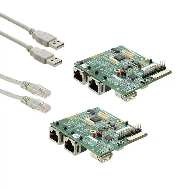
Figure 12. Sensor Extender Card
References
• RD1120, HiSPi-to-Parallel Sensor Bridge
• Aptina MT9M024 Data Sheet
• Aptina MT9M024 Register Reference Guide
Technical Support Assistance
Hotline: 1-800-LATTICE (North America)
+1-503-268-8001 (Outside North America)
e-mail: techsupport@latticesemi.com
Internet: www.latticesemi.com
Revision History
Date
Version
April 2013
01.0
Initial release.
Change Summary
October 2013
01.1
Changed access mode for programming the HDR60 to SPI Flash Background Programming.
20
�