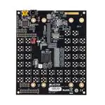
MachXO3L Breakout Board Evaluation Kit
User Guide
January 2015
EB94_1.1
�MachXO3L Breakout Board Evaluation Kit
Introduction
The MachXO3L Breakout Board Evaluation Kit focuses on providing an environment to evaluate high speed source
synchronous interfaces with the Lattice MachXO3L-2100 and MachXO3L-6900 products in both 49-ball WLCSP
and 256-ball caBGA packages respectively.
The MachXO3L Breakout Board contains two sections for development. The first section of the board features the
MachXO3L-2100 which is optimized for MIPI D-PHY receiver and MIPI D-PHY transmitter interfaces with up to four
data lanes and one clock lane each. The second section of the board features the MachXO3L-6900. This section
provides a flexible IO evaluation environment for MIPI D-PHY, SubLVDS, FPD-LINK, FPC-LINK as well as other
source synchronous type protocols. The IO of the MachXO3L-6900 provides eight high speed data and two high
speed clock interfaces in both transmit and receive directions. Connection to these interfaces is available through
SMAs for signal integrity and performance evaluation.
Evaluation Kit Contents
• MachXO3L Breakout Board
• Pre-loaded Demo
• Mini USB Cable
• QuickStart Guide
Figure 1. MachXO3L Breakout Board (Top Side)
Red LEDs (D5, D6, D7, D8) +
Tricolor LED (U8)
JTAG Chain Control Header (J50)
12V Supply
Source (J2)
MachXO3L-2100 (U9)
MachXO3L-2100 MIPI D-PHY
Output Connector (J49)
JTAG or USB Device
Programming
Power Regulators
5 V, 3.3 V, 2.5 V, 1.8 V, 1.2 V
MachXO3L-6900 PMOD (J47) and
General Purpose Connector (J16)
MachXO3L-6900 SMA Connectors
for Differential Output
MachXO3L-6900 SMA Connectors
for Differential Input
MachXO3L-6900 PMOD (J46) and
General Purpose Connector (J37)
MachXO3L-6900 (U7)
2
�MachXO3L Breakout Board Evaluation Kit
Figure 2. MachXO3L Breakout Board (Bottom Side)
MachXO3L-2000 MIPI D-PHY
Input Connector (J48)
Overview
The MachXO3L Breakout Board allows for multi-device testing and scalability by providing a larger MachXO3L6900 and a smaller MachXO3L-2100 device. The MachXO3L-6900 has two high speed clock and eight high speed
data inputs and outputs. By default these ports are configured for MIPI D-PHY IO support, but can be modified for
various IO options, such as LVDS, SubLVDS and CMOS. The MachXO3L-6900 also has four general purpose IO
headers, two of which have the ability to connect with Digilent PMOD interface boards. Additionally, the
MachXO3L-6900 device has the ability to control four general purpose LEDs and one tri-color RGB LED.
The MachXO3L-2100 is attached to two connectors providing four data and one clock lanes configured for MIPI DPHY going in to and out of the FPGA. The pinout for the MachXO3L-2100 is optimized for low cost and small form
factor by operating only off of 1.2 V and 3.3 V CMOS IO rails.
3
�MachXO3L Breakout Board Evaluation Kit
Figure 3. MachXO3L Breakout Board Functional Block Diagram
MIPI DSI Input Connector
MachXO3L-2100
MIPI DSI Output Connector
FTDI USB
Configuration
Controller
JTAG
Control
Header
Differential Input SMA’s
Pre-configured for MIPI D-PHY
General Purpose Header
RGB
LED
PMOD Header
MachXO3L-6900C
General Purpose Header
PMOD Header
LED
LED
LED
LED
Differential Output SMA’s
Pre-configured for MIPI D-PHY
MachXO3L Devices
The MachXO3L Breakout Board features both the MachXO3L-6900 in 256-ball caBGA package and the
MachXO3L-2100 in 49-ball WLCSP package. These devices feature 2100 and 6900 LUTs and 74 and 240 kbits of
embedded block RAM respectively. Both of these devices feature a variety of features and programmability. For
more information on the capabilities of each device see DS1047, MachXO3 Family Data Sheet.
4
�MachXO3L Breakout Board Evaluation Kit
Connector Descriptions
Configuration
The MachXO3L-2100 and MachXO3L-6900 parts can be programmed via JTAG through USB port or standalone
JTAG header. The USB path uses a FT2232H FTDI part to convert USB to JTAG. The standalone JTAG header
can be used to program the devices using the Lattice Programming Cable. In order to use the stand alone JTAG
header R5, R6, R7 and R8 to remove the FTDI part from the JTAG chain.
Power can be supplied to the board via mini USB port, 12 V power supply, from a separate board through the J48
DSI input connector or any combination of the three.
Figure 4. Configuration Connectors
USB
+ Supply
12 V Supply
(optional)
J1 – JTAG Header
Pin
1
2
3
4
5
6
7
8
Function
3.3 V
TDO
TDI
NC
NC
TMS
GND
TCK
J50 – JTAG Chain Control Header
Function
Pin
1
2
3
4
5
6
MachXO3L 2100 TDO
FTDI TDO
FTDI TDO
MachXO3L 6900 TDI
FTDI/MachXO3L 2100 TDI
MachXO3L 6900 TDO
JTAG Chain Options
2100 only
2100 + 6900
6900 only
1
2
3
4
5
6
1
2
3
4
5
6
1
2
3
4
5
6
5
�MachXO3L Breakout Board Evaluation Kit
MachXO3L-2100 MIPI D-PHY Connectors
The MachXO3L-2100 has input and output connectors capable of receiving and transmitting MIPI D-PHY, DSI or
CSI-2 data. The connectors are also capable of other IO standards with proper board modifications. Power can be
supplied to the MachXO3L board from the bottom input connector if desired. Similarly, power can be supplied from
the MachXO3L to any attached board through the top output connector.
Figure 5. MachXO3L-2100 MIPI D-PHY Connectors
Pin
1
3
5
7
9
11
13
15
17
19
21
23
25
27
29
31
33
35
37
39
41
43
45
47
49
J49 - Output Connector
Function
Function
DATA 0 P
DATA 0 N
GND
GND
DATA 1 P
DATA 1 N
GND
GND
CLOCK P
CLOCK N
GND
GND
DATA 2 P
DATA 2 N
GND
GND
DATA 3 P
DATA 3 N
GND
GND
GND
GND
Reserved
Reserved
Reserved
Reserved
Reserved
Reserved
GND
GND
GND
GND
12 V Output
12 V Output
12 V Output
12 V Output
5 V Output
5 V Output
5 V Output
5 V Output
3.3 V Output 3.3 V Output
3.3 V Output 3.3 V Output
GND
GND
GND
GND
GND
GND
Pin
2
4
6
8
10
12
14
16
18
20
22
24
26
28
30
32
34
36
38
40
42
44
46
48
50
Pin
1
3
5
7
9
11
13
15
17
19
21
23
25
27
29
31
33
35
37
39
41
43
45
47
49
6
J48 - Output Connector
Function
Function
DATA 0 P
DATA 0 N
GND
GND
DATA 1 P
DATA 1 N
GND
GND
CLOCK P
CLOCK N
GND
GND
DATA 2 P
DATA 2 N
GND
GND
DATA 3 P
DATA 3 N
GND
GND
GND
GND
Reserved
Reserved
Reserved
Reserved
Reserved
Reserved
GND
GND
GND
GND
12 V Output
12 V Output
12 V Output
12 V Output
5 V Output
5 V Output
5 V Output
5 V Output
3.3 V Output 3.3 V Output
3.3 V Output 3.3 V Output
GND
GND
GND
GND
GND
GND
Pin
2
4
6
8
10
12
14
16
18
20
22
24
26
28
30
32
34
36
38
40
42
44
46
48
50
�MachXO3L Breakout Board Evaluation Kit
MachXO3L-6900 PMOD and General Purpose Connectors
Two 0.1 inch 24-pin headers are available as general purpose connectors. Two 0.1 inch 12-pin headers are also
available either for general purpose or for use with Digilent PMOD boards.
Figure 6. MachXO3L-6900 PMOD and General Purpose Connectors
Pin
1
2
3
4
5
6
J47 - PMOD Header
Function Function Pin
PIO_G1 PIO_J2
7
PIO_H2 PIO_K1
8
PIO_H4 PIO_H5
9
PIO_J6 PIO_J4
10
GND
GND
11
VCCIO
VCCIO
12
Pin
1
2
3
4
5
6
J46 - PMOD Header
Function Function Pin
7
PIO_C15 PIO_J16
8
PIO_B16 PIO_J14
9
PIO_F13 PIO_J11
PIO_G12 PIO_L12 10
GND
11
GND
VCCIO
12
VCCIO
Pin
2
4
6
8
10
12
14
16
18
20
22
24
J16 - IO Header
Function Function Pin
3.3 V
3.3 V
1
PIO_P4 PIO_M8
3
PIO_T4 PIO_N9
5
PIO_T2 PIO_R9
7
PIO_R3 PIO_T10
9
PIO_P8 PIO_M9
11
PIO_T8 PIO_L10 13
PIO_M7 PIO_N10 15
PIO_N7 PIO_M11 17
PIO_M6 PIO_M10 19
PIO_L8 PIO_N11 21
GND
GND
23
Pin
2
4
6
8
10
12
14
16
18
20
22
24
J37- IO Header
Function Function Pin
VCCIO VCCIO
1
PIO_C4 PIO_F8
3
PIO_B5 PIO_D9
5
PIO_A4 PIO_B9
7
PIO_C5 PIO_A10
9
PIO_A5 PIO_F9
11
PIO_B6 PIO_E11 13
PIO_A3 PIO_D10 15
PIO_B4 PIO_E10 17
PIO_D8 PIO_C10 19
PIO_E9 PIO_F10 21
GND
GND
23
MachXO3L-6900 Input and Output SMA Connectors
The MachXO3L-6900 has 10 input SMA’s on bank 2 and 10 output SMA’s on bank 0. On the input side, two SMA’s
are connected to edge clock inputs allowing for high speed gearing. On the input side, the additional eight SMA
connections are connect to A/B pairs to support 1:8 gearing ratios. The clock and data lanes 0 and 1 have additional 50 ohm resistors connected to the P and N channels. These 50 ohm resistors are connected to bank 3 at
1.2V to support MIPI D-PHY contention detect and termination options.
On the transmit side each of the FPGA to SMA paths contain a resistor divider circuit. By default, the external resistor circuit is configured to support MIPI D-PHY in SLVS-200 and 1.2 V CMOS. The external circuit provides other
options such as subLVDS, and AC coupling options by providing additional board component pads for such modifications.
Software Requirements
You should install the following software before you begin to develop new designs for the MachXO3L Breakout
Board:
• Lattice Diamond® design software
• Diamond Standalone Programmer
7
�MachXO3L Breakout Board Evaluation Kit
Demonstration Design
Lattice provides a simple, pre-programmed demo to illustrate basic operation of the MachXO3L device. The design
flashes the red LEDs as well as the RGB LED. The design utilizes the internal oscillator operating at 12.09 MHz. A
counter is designed to slow down the clock and light up the individual LEDs. The demonstration design automatically starts on a newly purchased board when power is applied.
Figure 7. Demonstration Design Block Diagram
RGB
LED
Color
Select
BLUn
Internal Oscillator
(12.09 Mhz)
GRNn
Counter
REDn
PWM
Strobe
Stand Alone LED
Download Demo Designs
The LED demo is preprogrammed into the Breakout Board, however over time it is likely your board will be loaded
with a different design. Lattice distributes source and programming files for demonstration designs compatible with
the MachXO3L Breakout Board. The Lattice Diamond project and Verilog source code for the MachXO3L Breakout
Board example design can be obtained at www.latticesemi.com.
Programming Demonstration Design
1. Plug in USB Cable to USB J3 connector. Check that D3 LED is ON.
Figure 8. USB and D3 LED
LED
USB
2. Place a jumper on pins 4-5 and another jumper on pins 3-6 of the J50 JTAG header.
8
�MachXO3L Breakout Board Evaluation Kit
Figure 9. Pins 3-6 and J50 JTAG Header
3. Open Diamond Programmer Version 3.2 (or higher) and click OK. The board scans and the LCMXO3L-6900C
device becomes available for programming.
Figure 10. LCMXO3L-6900C Device for Programming
4. Double-click under Operation. The Device Properties dialog box opens.
9
�MachXO3L Breakout Board Evaluation Kit
Figure 11. SPI Flash Programming Access Mode
5. Select SPI Flash Programming in Access Mode.
6. Select the programming file RGB_test_impl1.bit.
7. Set all the SPI Flash Options as seen in Figure 23and click Load from File to retrieve the data file size. Then
click OK.
8. Click Design> Program. The External SPI Flash Programming operation completes successfully.
Figure 12. Operation Verified as Successful
9. Double-click under Operation. The Device Properties dialog box opens.
10
�MachXO3L Breakout Board Evaluation Kit
Figure 13. XNVCM Erase, Program, Verify, Feature Access Mode
10.Select XNVCM Erase, Program, Verify, Feature in Access Mode.
11.Select the programming file boot_from_SPIMaster.jed and click OK.
12.Click Design> Program. In the Output pane, verify that INFO – Operation: successful is displayed.
Figure 14. Operation Verified as Successful
13.Recycle power by unplugging and re-plugging in the USB cable. The Red LEDs and RGB LEDs start flashing.
Storage and Handling
Static electricity can shorten the lifespan of electronic components. Observe these tips to prevent damage that
could occur from electro-static discharge:
• Use anti-static precautions such as operating on an anti-static mat and wearing an anti-static wrist-band.
• Store the evaluation board in the packaging provided.
• Touch a metal USB housing to equalize voltage potential between you and the board.
11
�MachXO3L Breakout Board Evaluation Kit
Ordering Information
The MachXO3L breakout board can be ordered in two different forms. The MachXO3L SMA Breakout Board has all
of the SMA’s populated and the DSI connectors (J48 and J49) depopulated. The MachXO3L DSI Breakout Board
has all of the SMA’s de-populated and the DSI connectors (J48 and J49) populated.
Figure 15. MachXO3L SMA Breakout Board
12
�MachXO3L Breakout Board Evaluation Kit
Figure 16. MachXO3L DSI Breakout Board
Description
Ordering Part Number
MachXO3L SMA Breakout Board
LCMXO3L-SMA-EVN
MachXO3L DSI Breakout Board
LCMXO3L-DSI-EVN
China RoHS EnvironmentFriendly Use Period (EFUP)
Technical Support Assistance
e-mail:
techsupport@latticesemi.com
Internet: www.latticesemi.com
Revision History
Date
Version
Change Summary
January 2015
1.1
Updated Appendix A. Schematic Diagrams. Revised Figure 19, Board
Power.
August 2014
1.0
Initial release.
© 2015 Lattice Semiconductor Corp. All Lattice trademarks, registered trademarks, patents, and disclaimers are as
listed at www.latticesemi.com/legal. All other brand or product names are trademarks or registered trademarks of
their respective holders. The specifications and information herein are subject to change without notice.
13
�14
A
B
5
USB
CONNECTOR
4
USB to JTAG
USB to I2C
3
SMA INPUT
I/Os
Header
SPI
FLASH
I/Os
FPGA
BANK 1
BANK 2 & 3
FPGA
3
U9
LCMXO3L-2100E-5UWG49CTR
Optional JTAG
Configuration
PMOD
I/Os
BANK 4
U7
I/Os
LEDS(1-4)
LCMXO3L-6900C-6BG256C
I/Os
PMOD
May, 2014
BANK 0 & 5
I/Os
RGB LED
MachXO3L Breakout Board Revision B
MIPI_INPUT
C
4
MIPI_OUTPUT
2
Header
2
Optional I2C
Configuration
SMA OUTPUT
D
5
Date:
Size
C
May, 2014
1
Sheet
Lattice Semiconductor Applications
Email: techsupport@Latticesemi.com
Project
MachXO3L DSI Breakout Board
Title
Block Diagram
1
B
B
Schematic Rev
Board Rev
1
of 7
A
B
C
D
MachXO3L Breakout Board Evaluation Kit
Appendix A. Schematic Diagrams
Figure 17. Block Diagram
�A
B
5
8
7
6
5
0.1uF
C12
CS
CLK
DI
DO
93LC56-SO8
VCC
NU
ORG
VSS
U2
0.1uF
0.1uF
3.3V
C7
C6
C5
0.1uF
C8
1
2
3
4
0.1uF
3.3V
R16
10K
R17
10K
0.1uF
C9
R18
10K
R219
1K
3.3V
4
TP6
2
1
10uF
C13
18pF
C11
0.1uF
C10
FB_60ohm
PART_NUMBER = HI0603P600R-10
Manufacturer = Laird-signal
FB5
FB_60ohm
PART_NUMBER = HI0603P600R-10
Manufacturer = Laird-signal
FB4
C4
0.1uF
C3
4.7uF
3
12MHZ
3
4
R221
R218
0.1uF
3.3V
C2
C1
4.7uF
G1 G2
1
X1
1
2
1
2
3.3V
C14
18pF
12K
1K
[Pg3]
[Pg3]
DM
DP
13
3
2
63
62
61
6
14
7
8
49
50
3
FT2232H
3.3V
PWREN#
BCBUS0
BCBUS1
BCBUS2
BCBUS3
BCBUS4
BCBUS5
BCBUS6
BCBUS7
BDBUS0
BDBUS1
BDBUS2
BDBUS3
BDBUS4
BDBUS5
BDBUS6
BDBUS7
ACBUS0
ACBUS1
ACBUS2
ACBUS3
ACBUS4
ACBUS5
ACBUS6
ACBUS7
ADBUS0
ADBUS1
ADBUS2
ADBUS3
ADBUS4
ADBUS5
ADBUS6
ADBUS7
SUSPEND#
FTDI High-Speed USB
TEST
OSCO
OSCI
EECS
EECLK
EEDATA
REF
RESET#
DM
DP
VREGOUT
VREGIN
U1
FT2232HL
3
10
AGND
C
3.3V
4
4
9
VPHY
VPLL
12
37
64
VCORE
VCORE
VCORE
20
31
42
56
VCCIO
VCCIO
VCCIO
VCCIO
GND
GND
GND
GND
GND
GND
GND
GND
15
1
5
11
15
25
35
47
51
D
5
36
60
48
52
53
54
55
57
58
59
38
39
40
41
43
44
45
46
26
27
28
29
30
32
33
34
16
17
18
19
21
22
23
24
1
2
3
4
5
6
7
8
header_1x8
DNI
1
2
3
4
5
6
7
8
J1
VCCIO
1K
2
FTDI_TDO
XO3L_2100E_TDO
R217
1K
R216
VCCIO
Optional JTAG
Header when
VCCIO is 2.5V
2
R11
R12
R13
DNI
DNI
DNI
DNL
DNL
DNL
5
6
2
3
4.7K
1K
Date:
Optional I2C
Configuration
[Pg5,7]
[Pg5,7]
FTDI_TCK
Project
MachXO3L DSI Breakout Board
May, 2014
[Pg7]
[Pg5]
FTDI_TMS
FTDI_TDO
FTDI_TDI
1
Sheet
Lattice Semiconductor Applications
Email: techsupport@Latticesemi.com
XO3L_2100E_TDI
XO3L_6900C_TDO
FTDI_TDI
Title
USB to JTAG
Size
C
[Pg5]
[Pg5]
[Pg7]
[Pg7]
XO3L_6900C_TDI
SCL_1
SDA_1
R213
4.7K
R220
R212
SCL_2
SDA_2
Value = 3X2_HEADER
DEFAULT_OPTION = 1&4 and 3&6
4
1
J50
R203
R204
R205
R5
R6
R7
R8
0
0
0
0
0
0
0
4.7K
R211
VCCIO
1
B
B
Schematic Rev
Board Rev
2
of 7
A
B
C
D
MachXO3L Breakout Board Evaluation Kit
Figure 18. USB to JTAG
�A
B
C
C20
10uF
3
2
C127
680pF
R229
15K
12V
R230
34K
5
J2
12V DC JACK PWR
4
6
7
10
9
5
LT3680
EPAD
SW
BOOST
FB
BD
11
3
2
8
1
C128
L3
5V_Reg
C129
47uF
D12
Manufacturer = ON Semi
PART_NUMBER = MBRA340T3G
4.7uH
12V
0.47uF
R232
100K
RB496EA
D2
MIPI_VCC_12V_IN
R231
536K
LT3680
Manufacturer = Linear
PART_NUMBER = LT3680EDD#PBF
SYNC
PG
RT
VC
RUN_SS
VIN
U11
Jack_12V
4
J3
VCC
DD+
ID
GND
5V_Reg
SKT_MINIUSB_B_RA
VBUS_5V
0
0.1uF
R31
C17
0.1uF
C16
5V
0
R32
3.3V
DNI
R33
2.5V
VCCIO
VCCIO Select
- 3.3V Default
- 2.5V Optional
USB Power
1
2
3
4
5
600 Ohm 500 mA
L1
RB496EA
D1
DM
DP
1K
R30
[Pg2]
[Pg2]
D3
Green
5V Rail
1
2
1
5V Power Options
1) Regulated 5V Supply
2) USB 5V
3
R47
1M
R46
1M
10uF
1M
10uF
C45
R40
1M
R39
C27
5V
5V
21
12
19
11
20
18
17
14
13
21
12
19
11
20
18
17
14
13
THERMPAD
PWRGD2
PWRGD1
SHDN2
SHDN1
IN1_1
IN1_2
IN2_1
IN2_2
U6
THERMPAD
PWRGD2
PWRGD1
SHDN2
SHDN1
IN1_1
IN1_2
IN2_1
IN2_2
U5
GND1
16
12V Power Options
1) External 12V DC Supply
2) Signet Main Board Connector
3
10
9
8
7
1
2
4
3
C25
0.01uF
C40
0.01uF
2
10
9
8
7
1
2
4
3
C44
2
C38
R51
113K
C57
210K
R53
R49
237K
243K
127
R43
1.22V
R41
4.7uF
255K
R48
357K
R37
0.01uF
0.01uF
LT3030EFE#TRPBF
ADJ2
BYP2
OUT2_2
OUT2_1
ADJ1
BYP1
OUT1_2
OUT1_1
LT3030EFE#TRPBF
ADJ2
BYP2
OUT2_2
OUT2_1
ADJ1
BYP1
OUT1_2
OUT1_1
GND4
6
D
4
GND2
15
GND1
16
GND4
GND3
5
GND2
15
GND3
5
16
6
5
TP33L
TP12H
R42
TP12L
R44
TP25L
127
R52
127
0.1
R50
TP18L
Date:
Size
C
May, 2014
TP1
C49
0.1uF
1.8V
2.5V
1.2V
3.3V
1
Sheet
B
B
Schematic Rev
Board Rev
3
of 7
1.8V Rail
2.5V Rail
1.2V Rail
3.3V Rail
TP_LOOP_BLACK
TP5
TP_LOOP_RED
TP3
TP_LOOP_RED
0.1uF
C26
1
1
1
Lattice Semiconductor Applications
Email: techsupport@Latticesemi.com
22uF
C59
22uF
Project
MachXO3L DSI Breakout Board
Title
Board Power
0.1 OHM 1/2W 1% 0805
TP18H
0.1
R45 0.1 OHM 1/2W 1% 0805
TP25H
C48
22uF
C39
22uF
C30
Current Sense TP
2.51V
4.7uF
C58
R36
0.1
0.1 OHM 1/2W 1% 0805
TP33H
0.1
0.1 OHM 1/2W 1% 0805
127
R38
1.81V
10uF
C43
10uF
C29
3.31V
Current Sense TP
5V
12V
Test Points
1
A
B
C
D
MachXO3L Breakout Board Evaluation Kit
Figure 19. Board Power
�A
B
C
[Pg4]
SCLK_256
MISO_256
DIN1_LP_P
DIN1_HS_P
DIN1_HS_N
DIN1_LP_N
PIO_M7
PIO_N7
PIO_M6
PIO_L8
[Pg4]
[Pg4]
[Pg4]
[Pg4]
[Pg4]
[Pg4]
[Pg4]
[Pg4]
[Pg4]
[Pg4]
[Pg4]
[Pg4]
R61
51
3.3V
0.1uF
R227
C130
30pF
20
Place close to U7
Place close to U10
SCLK_256
C64
R60
R59
51
51
R58
51
[Pg4]
[Pg4]
[Pg4]
[Pg4]
[Pg4]
[Pg4]
5
K8
K9
N8
L9
P8
T8
T7
R8
M6
L8
M7
N7
R7
P7
P6
T6
N6
L7
T5
R6
T3
R4
R5
P5
T2
R3
LCMXO3L-6900C-6BG256C
DIN1_LP_P
DIN1_LP_N
CLKIN1_LP_P
CLKIN1_LP_N
SSn_256
MOSI_256
1
3
6
5
K5
L4
K4
L5
L1
L3
L2
M1
CS
WP
SCK
SDI
U10
7
2
4
[Pg4]
51
51
51
51
PL14C/PL20C/PL25C
PL14D/PL20D/PL25D
PL14A/PL20A/PL25A
PL14B/PL20B/PL25B
PL13A/PL19A/PL24A
PL13B/PL19B/PL24B
PL13C/PL18C/PL23C
PL13D/PL18D/PL23D
MISO_256
N5
N12
T15
R14
R12
P13
P12
T13
R11
T12
R13
T14
M10
N11
T11
P11
P10
R10
N10
M11
M9
L10
R9
T10
T9
P9
M8
N9
LCMXO3L-6900C-6BG256C
2K/4K/7K || 2nd_Fn.
4
VCCIO3/VCCIO3/VCCIO3
PL12A/PL17A/PL22A || PCLKT3_0
PL12B/PL17B/PL22B || PCLKC3_0
PL12C/PL17C/PL21C
PL12D/PL17D/PL21D
PL11C/PL16C/PL19C
PL11D/PL16D/PL19D
PL11A/PL16A/PL19A
PL11B/PL16B/PL19B
U7D
M25PX16-VMN6TP
HOLD
SDO
BANK3
VCCIO2/VCCIO2/VCCIO2
VCCIO2/VCCIO2/VCCIO2
PB25C/PB30C/PB38C
PB25D/PB30D/PB38D
PB25A/PB30A/PB38A || SN
PB25B/PB30B/PB38B || SI/SISPI
PB24A/PB29A/PB37A
PB24B/PB29B/PB37B
PB22A/PB27A/PB35A
PB22B/PB27B/PB35B
PB22C/PB26A/PB34A
PB22D/PB26B/PB34B
PB21C/PB24C/PB31C
PB21D/PB24D/PB31D
PB21A/PB24A/PB31A
PB21B/PB24B/PB31B
PB19A/PB23A/PB29A
PB19B/PB23B/PB29B
PB19C/PB23C/PB28A
PB19D/PB23D/PB28B
PB18C/PB21C/PB26C
PB18D/PB21D/PB26D
PB18A/PB21A/PB26A
PB18B/PB21B/PB26B
2K/4K/7K || 2nd_Fn.
VCCIO2/VCCIO2/VCCIO2
VCCIO2/VCCIO2/VCCIO2
PB12C/PB15C/PB18C
PB12D/PB15D/PB18D
PB12A/PB15A/PB18A
PB12B/PB15B/PB18B
PB11A/PB13A/PB16A || PCLKT2_0
PB11B/PB13B/PB16B || PCLKC2_0
PB11C/PB12A/PB15A
PB11D/PB12B/PB15B
PB9C/PB10C/PB13C
PB9D/PB10D/PB13D
PB9A/PB10A/PB13A
PB9B/PB10B/PB13B
PB16C/PB18A/PB21A
PB16D/PB18B/PB21B
PB16A/PB20A/PB23A || PCLKT2_1
PB16B/PB20B/PB23B || PCLKC2_1
PB8A/PB9A/PB12A || MCLK/CCLK
PB8B/PB9B/PB12B || SO/SPISO
PB8C/PB9C/PB10A
PB8D/PB9D/PB10B
PB6A/PB7A/PB9A
PB6B/PB7B/PB9B
PB6C/PB6A/PB7A
PB6D/PB6B/PB7B
PB5A/PB4A/PB6A || CSSPIN
PB5B/PB4B/PB6B
PB3C/PB3C/PB4C
PB3D/PB3D/PB4D
BANK2
XO3L Configuration SPI Flash
0.1uF 0.1uF
C63
C122
[Pg4]
CLKIN1_LP_P
[Pg4]
CLKIN1_HS_P
[Pg4]
CLKIN1_HS_N
[Pg4]
CLKIN1_LP_N
[Pg4]
PIO_P8
[Pg4]
PIO_T8
DIN5_HS_P
DIN5_HS_N
DIN3_HS_P
DIN3_HS_N
[Pg4]
[Pg4]
DIN7_HS_P
DIN7_HS_N
SSn_256
[Pg4]
[Pg4]
PIO_T2
PIO_R3
[Pg4]
R197
[Pg4]
[Pg4]
PB3A/PB3A/PB4A
PB3B/PB3B/PB4B
R196
1k
PIO_P4
PIO_T4
U7C
R195
1k
4.7K
[Pg4]
[Pg4]
P4
T4
Place close to U10
D
5
MIPI RX Termination
8
VCC
GND
4
R194
1k
M4
R1
P2
M2
N3
M3
N1
N2
P1
0
VCCIO
MOSI_256
[Pg4]
[Pg4]
[Pg4]
[Pg4]
[Pg4]
[Pg4]
[Pg4]
[Pg4]
[Pg4]
[Pg4]
C71
C70
0.1uF 1uF
R65
0
1.2V
PIO_P4
PIO_T4
PIO_T2
PIO_R3
PIO_P8
PIO_T8
PIO_M7
PIO_N7
PIO_M6
PIO_L8
DIN0_LP_P
DIN0_LP_N
CLKIN0_LP_P
CLKIN0_LP_N
3.3V
[Pg4]
[Pg4]
[Pg4]
[Pg4] VCCIO
[Pg4]
DIN6_HS_P
DIN6_HS_N
[Pg4]
[Pg4]
DIN4_HS_P
DIN4_HS_N
DNI
1
3
5
7
9
11
13
15
17
19
21
23
DNI
HEADER 12X2
[Pg4]
[Pg4]
[Pg4]
[Pg4]
2
4
6
8
10
12
14
16
18
20
22
24
J16
3.3V
3
PIO_M8
PIO_N9
PIO_R9
PIO_T10
PIO_M9
PIO_L10
PIO_N10
PIO_M11
PIO_M10
PIO_N11
Pull-up resistor R62 is for
cases where I2C is used. If
I2C is not used for programming
this pull-up is not required.
IO Header
R222
R62
4.7K
[Pg4]
[Pg4]
PIO_M10
PIO_N11
[Pg4]
[Pg4]
[Pg4]
[Pg4]
[Pg4]
[Pg4]
[Pg4]
[Pg4]
DIN2_HS_P
DIN2_HS_N
PIO_N10
PIO_M11
DIN0_LP_P
DIN0_HS_P
DIN0_HS_N
DIN0_LP_N
PIO_M9
PIO_L10
C67
C66
C61
0.1uF 0.1uF 1uF
R57
R56
R55
R54
PIO_M8
[Pg4]
PIO_N9
[Pg4]
CLKIN0_LP_P
[Pg4]
CLKIN0_HS_P
[Pg4]
CLKIN0_HS_N
[Pg4]
CLKIN0_LP_N
[Pg4]
PIO_R9
[Pg4]
PIO_T10
[Pg4]
3
[Pg4]
[Pg4]
[Pg4]
[Pg4]
[Pg4]
[Pg4]
[Pg4]
[Pg4]
[Pg4]
[Pg4]
J23
SMA73391-0060
J21
SMA73391-0060
J19
SMA73391-0060
J17
SMA73391-0060
J14
SMA73391-0060
J12
SMA73391-0060
J10
SMA73391-0060
J8
SMA73391-0060
J6
SMA73391-0060
J4
SMA73391-0060
2
1
1
1
1
1
1
1
1
1
1
1
1
1
1
1
1
1
1
1
1
[Pg4]
[Pg4]
[Pg4]
DIN0_HS_N
DIN2_HS_P
J15
SMA73391-0060
J13
SMA73391-0060
J11
SMA73391-0060
J9
SMA73391-0060
J7
[Pg4] SMA73391-0060
CLKIN0_HS_N
DIN0_HS_P
J5
[Pg4] SMA73391-0060
CLKIN0_HS_P
SMA Connectors
2
[Pg4]
[Pg4]
[Pg4]
[Pg4]
[Pg4]
DIN2_HS_N
DIN4_HS_P
DIN4_HS_N
DIN6_HS_P
DIN6_HS_N
2
J24
SMA73391-0060
J22
SMA73391-0060
J20
SMA73391-0060
J18
SMA73391-0060
4
R64
3
3
4
4
2
5
5
2
2
3
3
4
4
3
5
5
2
2
5
5
3
4
4
3
3
2
2
5
5
4
4
3
3
2
2
5
3
4
4
5
5
2
2
3
3
4
4
5
5
2
2
3
3
4
4
3
5
5
2
2
5
3
4
4
3
5
2
2
5
5
3
4
4
2
3
4
3
2
5
2
1
2
5
5
3
4
4
3
3
2
1
2
5
5
2
4
4
3
3
4
4
1
2
5
5
2
1
2
3
3
4
4
5
5
2
1
2
3
3
4
4
5
5
3
3
2
1
2
5
5
4
4
3
3
2
1
2
5
5
2
4
4
3
3
4
4
1
2
5
5
2
1
2
3
3
4
4
5
5
2
1
2
5
3
3
4
4
17
5
Place resistors as close to the bank 2 pins on XO3 as possible.
Arrange them so they do not influence the *HS* trace path.
Match trace length for all P and N signals. Match lengths between HS signals, match lengths between LP signals.
1
1
1
1
1
1
1
1
1
1
[Pg4]
[Pg4]
[Pg4]
DIN5_HS_N
DIN7_HS_P
DIN7_HS_N
Date:
Size
C
May, 2014
1
Sheet
Lattice Semiconductor Applications
Email: techsupport@Latticesemi.com
Project
MachXO3L DSI Breakout Board
Title
DSI: SMA_INPUT
[Pg4]
DIN5_HS_P
[Pg4]
DIN3_HS_P
[Pg4]
[Pg4]
DIN1_HS_N
DIN3_HS_N
[Pg4]
[Pg4]
CLKIN1_HS_N
DIN1_HS_P
[Pg4]
CLKIN1_HS_P
1
B
B
Schematic Rev
Board Rev
4
of 7
A
B
C
D
MachXO3L Breakout Board Evaluation Kit
Figure 20. DSI: SMA_INPUT
�A
B
C
D
5
J44
SMA73391-0060
J43
SMA73391-0060
J40
SMA73391-0060
J38
SMA73391-0060
J35
SMA73391-0060
J33
SMA73391-0060
J31
SMA73391-0060
J29
SMA73391-0060
J27
SMA73391-0060
J25
SMA73391-0060
2
1
2
5
3
3
4
4
1
1
1
1
1
1
1
1
1
1
1
1
1
1
1
1
1
1
1
J39
[Pg5] SMA73391-0060
J41
[Pg5] SMA73391-0060
J42
[Pg5] SMA73391-0060
J45
[Pg5] SMA73391-0060
DOUT4_P
DOUT4_N
DOUT6_P
DOUT6_N
DOUT2_P
J36
[Pg5] SMA73391-0060
J34
[Pg5] SMA73391-0060
DOUT0_N
DOUT2_N
J32
[Pg5] SMA73391-0060
DOUT0_P
J28
SMA73391-0060
[Pg5]
CLKOUT0_N
J30
[Pg5] SMA73391-0060
J26
SMA73391-0060
[Pg5]
CLKOUT0_P
2
1
2
5
3
3
4
4
1
1
1
1
1
1
1
1
1
1
1
1
1
1
1
1
1
1
1
4
CLKOUT0_N
DOUT7_N
DOUT6_N
[Pg5]
[Pg5]
DOUT6_P
[Pg5]
DOUT7_P
[Pg5]
[Pg5]
DOUT4_N
[Pg5]
DOUT5_N
DOUT4_P
[Pg5]
DOUT5_P
DOUT2_N
DOUT2_P
[Pg5]
[Pg5]
DOUT3_N
[Pg5]
[Pg5]
[Pg5]
DOUT3_P
DOUT0_N
[Pg5]
[Pg5]
DOUT0_P
[Pg5]
[Pg5]
DOUT1_N
DOUT1_P
[Pg5]
[Pg5]
CLKOUT1_N
CLKOUT0_P
[Pg5]
[Pg5]
CLKOUT1_P
2
CLKOUT1_N
[Pg5]
[Pg5]
[Pg5]
CLKOUT1_P
[Pg5]
DOUT0_HS_N [Pg5] [Pg5] DOUT1_N
DOUT0_LP_N
[Pg5]
DOUT0_LP_P
[Pg5]
DOUT0_HS_P [Pg5] [Pg5] DOUT1_P
[Pg5]
CLKOUT0_HS_N
CLKOUT0_LP_N
CLKOUT0_LP_P
CLKOUT0_HS_P
[Pg5]
3
R132
DOUT6_HS_N [Pg5] [Pg5] DOUT7_N
330
DOUT6_LP_N
[Pg5]
30
R134
R126
DOUT6_LP_P
[Pg5]
30
DOUT6_HS_P [Pg5] [Pg5] DOUT7_P
330
R128
R118
DOUT4_HS_N [Pg5] [Pg5] DOUT5_N
330
DOUT4_LP_N
[Pg5]
30
R120
R112
DOUT4_LP_P
[Pg5]
30
DOUT4_HS_P [Pg5] [Pg5] DOUT5_P
330
R114
R104
DOUT2_HS_N [Pg5] [Pg5] DOUT3_N
330
DOUT2_LP_N
[Pg5]
30
R106
R98
DOUT2_LP_P
[Pg5]
30
DOUT2_HS_P [Pg5] [Pg5] DOUT3_P
330
R100
R88
330
30
R90
R82
30
330
R84
R74
330
30
R76
R68
30
330
R70
DOUT1_HS_N
DOUT1_LP_N
DOUT1_LP_P
DOUT1_HS_P
CLKOUT1_HS_N
CLKOUT1_LP_N
CLKOUT1_LP_P
CLKOUT1_HS_P
DOUT3_HS_N
DOUT3_LP_N
R133
DOUT7_HS_N
330
DOUT7_LP_N
30
R135
R127
DOUT7_LP_P
30
DOUT7_HS_P
330
R129
R119
DOUT5_HS_N
330
DOUT5_LP_N
30
R121
R113
DOUT5_LP_P
30
DOUT5_HS_P
330
R115
R105
330
30
R107
R99
DOUT3_LP_P
30
DOUT3_HS_P
330
R101
R89
330
30
R91
R83
30
330
R85
R75
330
30
R77
R69
30
330
R71
[Pg5]
[Pg5]
[Pg5]
[Pg5]
[Pg5]
[Pg5]
[Pg5]
[Pg5]
[Pg5]
[Pg5]
[Pg5]
[Pg5]
[Pg5]
[Pg5]
[Pg5]
[Pg5]
[Pg5]
[Pg5]
[Pg5]
[Pg5]
[Pg5]
[Pg5]
[Pg5]
[Pg5]
[Pg5]
[Pg5]
[Pg5]
[Pg5]
PIO_A5
PIO_B6
PIO_A3
PIO_B4
[Pg5]
[Pg5]
[Pg5]
[Pg5]
FTDI_TCK
FTDI_TMS
C74
PIO_D8
PIO_E9
DOUT4_LP_P
DOUT4_LP_N
DOUT2_LP_P
DOUT2_LP_N
[Pg5]
[Pg5]
[Pg5]
[Pg5]
VCCIO
[Pg5]
[Pg5]
D5
D12
D8
E9
C8
A8
A7
B8
F7
E8
E6
D7
B7
C7
C6
A6
D6
E7
A3
B4
A5
B6
A4
C5
B3
C4
B5
2
4
6
8
10
12
14
16
18
20
22
24
1
3
5
7
9
11
13
15
17
19
21
23
DNI
2
HEADER 12X2
J37
F4
G6
E1
F2
C1
D2
E2
E3
D3
D1
B1
C2
BANK5
PIO_F8
PIO_D9
PIO_B9
PIO_A10
PIO_F9
PIO_E11
PIO_D10
PIO_E10
PIO_C10
PIO_F10
[Pg5]
[Pg5]
[Pg5]
[Pg5]
[Pg5]
[Pg5]
[Pg5]
[Pg5]
[Pg5]
[Pg5]
LCMXO3L-6900C-6BG256C
VCCIO
E4
F5
H6
G2
G3
F3
F1
G8
G9
A13
C13
B14
A15
C12
B12
B13
A14
B11
A12
F10
D11
A11
C11
C10
B10
D10
E10
F9
E11
B9
A10
A9
C9
F8
D9
Date:
Size
C
May, 2014
1
[Pg5]
[Pg5]
0
VCCIO
CLKOUT1_HS_P
CLKOUT1_HS_N
DOUT1_HS_P
DOUT1_HS_N
[Pg5]
[Pg5]
[Pg5]
[Pg5]
1
Sheet
Lattice Semiconductor Applications
Email: techsupport@Latticesemi.com
C82
C83
0.1uF 1uF
0
1.2V
CLKOUT1_LP_P
CLKOUT1_LP_N
DOUT3_LP_P
DOUT3_LP_N
[Pg5]
[Pg5]
[Pg5]
[Pg5]
DOUT7_LP_P
DOUT7_LP_N
DOUT5_LP_P
DOUT5_LP_N
[Pg5]
[Pg5]
[Pg5]
[Pg5]
[Pg5]
[Pg5]
[Pg5]
[Pg5]
DOUT5_HS_P
DOUT5_HS_N
[Pg5]
[Pg5]
DOUT3_HS_P
DOUT3_HS_N
[Pg5]
DOUT7_HS_P
DOUT7_HS_N
[Pg5]
[Pg5]
[Pg5]
[Pg5]
[Pg5]
[Pg2]
[Pg2]
C77
C78
C79
0.1uF 0.1uF 1uF
PIO_F10
PIO_C10
PIO_D10
PIO_E10
PIO_F9
PIO_E11
[Pg5]
[Pg5]
SCL_1
SDA_1
PIO_B9
PIO_A10
PIO_F8
PIO_D9
Project
MachXO3L DSI Breakout Board
Title
DSI: SMA_OUTPUT
VCCIO5/VCCIO5/VCCIO5
PL5C/PL8C/PL9C
PL5D/PL8D/PL9D
PL5A/PL8A/PL9A
PL5B/PL8B/PL9B
PL4A/PL7A/PL8A
PL4B/PL7B/PL8B
PL4C/PL7C/PL7C
PL4D/PL7D/PL7D
G5
G4
VCCIO0/VCCIO0/VCCIO0
VCCIO0/VCCIO0/VCCIO0
* = TRUE LVDS Output
2K/4K/7K || 2nd_Fn.
PL3A/PL6A/PL6A || PCLKT5_0
PL3B/PL6B/PL6B || PCLKC5_0
PL3C/PL6C/PL6C
PL3D/PL6D/PL6D
PT24A*/PT28A*/PT36A*
PT24B*/PT28B*/PT36B*
PT23A*/PT27A*/PT35A*
PT23B*/PT27B*/PT35B*
PT22C/PT26A*/PT34A*
PT22D/PT26B*/PT34B*
PT22A*/PT25A*/PT33A*
PT22B*/PT25B*/PT33B*
PT21C/PT24C/PT32A*
PT21D/PT24D/PT32B*
PT21A*/PT24A*/PT28A*
PT21B*/PT24B*/PT28B*
2K/4K/7K || 2nd_Fn.
PL2A/PL4A/PL4A || L_GPLLT_IN
PL2B/PL4B/PL4B || L_GPLLC_IN
PL2C/PL4C/PL4C
PL2D/PL4D/PL4D
PT20A*/PT23A*/PT27A*
PT20B*/PT23B*/PT27B*
PT19C/PT22A*/PT26A*
PT19D/PT22B*/PT26B*
PT19A*/PT21A*/PT25A*
PT19B*/PT21B*/PT25B*
PT24C/PT28C/PT36C || INITN
PT24D/PT28D/PT36D || DONE
PL1A/PL3A/PL3A || L_GPLLT_FB
PL1B/PL3B/PL3B || L_GPLLC_FB
PL1C/PL2C/PL2C
PL1D/PL2D/PL2D
U7F
LCMXO3L-6900C-6BG256C
VCCIO0/VCCIO0/VCCIO0
VCCIO0/VCCIO0/VCCIO0
PT17C/PT19A*/PT21A*
PT17D/PT19B*/PT21B*
PT18A*/PT20A*/PT22A*
PT18B*/PT20B*/PT22B*
PT20C/PT23C/PT27C || JTAGENB
PT20D/PT23D/PT27D || PROGRAMN
PT17A*/PT18A*/PT18A* || PCLKT0_1
PT17B*/PT18B*/PT18B* || PCLKC0_1
PT16C/PT15C/PT17C || TCK
PT16D/PT15D/PT17D || TMS
PT16A*/PT15A*/PT17A*
PT16B*/PT15B*/PT17B*
PT13C/PT14C/PT16A*
PT13D/PT14D/PT16B*
PT13A*/PT14A*/PT15A*
PT13B*/PT14B*/PT15B*
BANK0
PT18C/PT20C/PT22C || SCL/PCLKT0_0
PT18D/PT20D/PT22D || SDA/PCLKC0_0
PT12C/PT13C/PT14C || TDO
PT12D/PT13D/PT14D || TDI
PT12A*/PT13A*/PT14A*
PT12B*/PT13B*/PT14B*
PT11C/PT12A*/PT12A*
PT11D/PT12B*/PT12B*
PT11A*/PT11A*/PT11A*
PT11B*/PT11B*/PT11B*
PT10A*/PT10A*/PT10A*
PT10B*/PT10B*/PT10B*
PT9C/PT9C/PT9C
PT9A*/PT9A*/PT9A*
PT9B*/PT9B*/PT9B*
U7A
IO Header
CLKOUT0_LP_P
CLKOUT0_LP_N
DOUT0_LP_P
DOUT0_LP_N
DOUT6_LP_P
DOUT6_LP_N
[Pg5]
[Pg5]
[Pg5]
[Pg5]
DOUT1_LP_P
DOUT1_LP_N
[Pg5]
[Pg5]
0.1uF 0.1uF
C73
[Pg5]
[Pg5]
CLKOUT0_HS_P
CLKOUT0_HS_N
[Pg2,7]
[Pg2,7]
PIO_C4
PIO_B5
PIO_A4
PIO_C5
PIO_A5
PIO_B6
PIO_A3
PIO_B4
PIO_D8
PIO_E9
[Pg5]
[Pg5]
DOUT0_HS_P
DOUT0_HS_N
DOUT2_HS_P
DOUT2_HS_N
[Pg5]
[Pg5]
[Pg5]
[Pg5]
DOUT4_HS_P
DOUT4_HS_N
XO3L_6900C_TDO
XO3L_6900C_TDI
DOUT6_HS_P
DOUT6_HS_N
PIO_A4
PIO_C5
PIO_C4
PIO_B5
[Pg5]
[Pg5]
[Pg5]
[Pg5]
[Pg5]
[Pg5]
[Pg7]
[Pg2]
[Pg5]
[Pg5]
[Pg5]
[Pg5]
Place resistors as close to the bank 0 pins on XO3 as possible.
Arrange them so they do not influence the *HS* trace path.
Match trace length for all P and N signals. Match lengths between HS signals, match lengths between LP signals.
MIPI TX Termination
3
R67
R79
SMA Connectors
4
R72
R86
5
2
2
3
3
4
4
5
5
2
2
3
3
4
4
5
5
2
2
3
3
4
4
5
5
2
2
3
3
4
4
5
5
2
2
3
3
4
4
5
5
2
2
3
3
4
4
5
5
2
2
3
3
4
4
5
5
2
2
3
3
4
4
5
5
2
2
3
3
4
4
5
5
R73
R87
5
2
2
3
3
4
4
5
5
2
2
3
3
4
4
5
5
2
2
3
3
4
4
5
5
2
2
3
3
4
4
5
5
2
2
3
3
4
4
5
5
2
2
3
3
4
4
5
5
2
2
3
3
4
4
5
5
2
2
3
3
4
4
5
5
2
2
3
3
4
4
5
5
R66
R78
R92
R96
R80
DNI
DNI
DNI
DNI
DNI
R108
R110
DNI
DNI
DNI
R93
R97
R81
DNI
DNI
R109
DNI
DNI
DNI
DNI
DNI
R102
R116
R130
DNI
DNI
DNI
DNI
DNI
R122
R124
R136
DNI
DNI
DNI
DNI
DNI
R103
R117
R131
DNI
DNI
DNI
DNI
R111
R123
R125
R137
R138
18
DNI
R95
B
B
Schematic Rev
Board Rev
5
of 7
C123
DNL
10uF
100K
VCCIO
R225
5
A
B
C
D
MachXO3L Breakout Board Evaluation Kit
Figure 21. DSI: SMA_OUTPUT
�19
A
B
C
PIO_F13
PIO_G12
PIO_J16
PIO_J14
PIO_J11
PIO_L12
[Pg6]
[Pg6]
[Pg6]
[Pg6]
PIO_C15
PIO_B16
[Pg6]
[Pg6]
[Pg6]
[Pg6]
5
C89
C90
0.1uF 0.1uF
B2
B15
C3
C14
D4
D13
E5
E12
F6
F11
H8
H9
J8
J9
L6
L11
M5
M12
N4
N13
P3
P14
R2
R15
E13
H10
P15
R16
N15
P16
K11
L13
J11
L12
H11
J13
J16
J14
H13
J12
G11
H12
F12
G13
F13
G12
C16
D15
C15
B16
DQ1
PR14A/PR19A/PR24A
PR14B/PR19B/PR24B
PR13A/PR18A/PR23A
PR13B/PR18B/PR23B
PR12A/PR16A/PR21A
PR12B/PR16B/PR21B
PR11C/PR15C/PR19C
PR11D/PR15D/PR19D
PR11A/PR15A/PR18A
PR11B/PR15B/PR18B
PR10A/PR14A/PR17A
PR10B/PR14B/PR17B
PR9A/PR13A/PR16A DQS1
PR9B/PR13B/PR16B DQS1N
LCMXO3L-6900C-6BG256C
LCMXO3L-6900C-6BG256C
2K/4K/7K
GND/GND/GND
GND/GND/GND
GND/GND/GND
GND/GND/GND
GND/GND/GND
GND/GND/GND
GND/GND/GND
GND/GND/GND
GND/GND/GND
GND/GND/GND
GND/GND/GND
GND/GND/GND
GND/GND/GND
GND/GND/GND
GND/GND/GND
GND/GND/GND
GND/GND/GND
GND/GND/GND
GND/GND/GND
GND/GND/GND
GND/GND/GND
GND/GND/GND
GND/GND/GND
GND/GND/GND
NC/NC/NC
VCC/VCC/VCC
VCC/VCC/VCC
VCC/VCC/VCC
VCC/VCC/VCC
VCC/VCC/VCC
VCC/VCC/VCC
VCC/VCC/VCC
VCC/VCC/VCC
A2
A1
A16
G7
G10
K7
K10
T1
T16
J10
M13
N16
N14
M14
M15
L15
M16
K13
K12
L16
L14
K14
K15
J15
K16
H14
H16
G16
H15
G15
G14
F14
F16
E16
F15
D16
E14
D14
E15
LED_RED
0
3.3V
C93
C94
C95
0.1uF 0.1uF 1uF
4
0
[Pg6]
[Pg6]
[Pg6]
[Pg6]
PIO_H4
PIO_J6
[Pg6]
[Pg6]
VCCIO
LED3
LED4
LED1
LED2
LED_GREEN
LED_BLUE
C97
C98
C99
C96
0.1uF 0.1uF 0.1uF 1uF
VCCIO1/VCCIO1/VCCIO1
VCCIO1/VCCIO1/VCCIO1
2K/4K/7K || 2nd_Fn.
VCCIO1/VCCIO1/VCCIO1
VCCIO1/VCCIO1/VCCIO1
U7G
PR6A/PR9A/PR11A DQS0
PR6B/PR9B/PR11B DQS0N
PR5A/PR8A/PR9A
PR5B/PR8B/PR9B
PR4A/PR6A/PR7A
PR4B/PR6B/PR7B
PR3A/PR5A/PR5A
PR3B/PR5B/PR5B
PR7A/PR10A/PR12A || PCLKT1_0
PR7B/PR10B/PR12B || PCLKC1_0
DQ0
PR2A/PR3A/PR3A || R_GPLLT_IN**
PR2B/PR3B/PR3B || R_GPLLC_IN**
PR1A/PR2A/PR2A || R_GPLLT_FB**
PR1B/PR2B/PR2B || R_GPLLC_FB**
** = 2nd_Fn. applicable for 4K and 7K devices only.
PR14C/PR20C/PR25C
PR14D/PR20D/PR25D
PR13C/PR18C/PR23C
PR13D/PR18D/PR23D
PR12C/PR16C/PR21C
PR12D/PR16D/PR21D
PR10C/PR14C/PR17C
PR10D/PR14D/PR17D
PR9C/PR13C/PR16C
PR9D/PR13D/PR16D
PR7C/PR10C/PR15A
PR7D/PR10D/PR15B
PR6C/PR9C/PR11C
PR6D/PR9D/PR11D
PR5C/PR8C/PR10C
PR5D/PR8D/PR10D
PR4C/PR6C/PR7C
PR4D/PR6D/PR7D
PR3C/PR5C/PR6C
PR3D/PR5D/PR6D
PR2C/PR4C/PR4C
PR2D/PR4D/PR4D
PR1C/PR2C/PR2C
PR1D/PR2D/PR2D
PIO_G1
PIO_H2
[Pg6]
[Pg6]
PIO_C15
PIO_B16
PIO_F13
PIO_G12
U7E
PL9A/PL13A/PL15A
PL9B/PL13B/PL15B
PL10A/PL14A/PL17A
PL10B/PL14B/PL17B
PL10C/PL14C/PL16C
PL10D/PL14D/PL16D
PL9C/PL13C/PL15C
PL9D/PL13D/PL15D
BANK4
3
[Pg6]
[Pg6]
[Pg6]
[Pg6]
PIO_G1
PIO_H2
PIO_H4
PIO_J6
110
R152
3
2
1
4
5
6
2
2
2
2
1
2
3
4
5
6
J47
7
8
9
10
11
12
D5
Red
VCCIO
5V
D6
Red
1K
R141
LEDs
PIO_J2
PIO_K1
PIO_H5
PIO_J4
1
CDBU0520
1
CDBU0520
D11
1
CDBU0520
D10
D9
R140
1K
SFT722N-S
MFG = Seoul
MFG P/N = SFT722N-S
U8
PMOD Connector
62
VCCIO
62
R151
DNI
[Pg6]
[Pg6]
[Pg6]
[Pg6]
LED_RED
LED_GREEN
LED_BLUE
RGB LED
LED4
LED3
LED2
LED1
PMOD 2x6
PIO_J16
PIO_J14
PIO_J11
PIO_L12
0
C85
C87
C86
0.1uF 0.1uF 1uF
R150
[Pg6]
[Pg6]
PIO_H5
PIO_J4
VCCIO
[Pg6]
[Pg6]
PIO_J2
PIO_K1
DNI
7
8
9
10
11
12
H7
J7
K3
K2
J5
K6
H5
J4
J2
K1
PMOD 2x6
1
2
3
4
5
6
J46
VCCIO
PMOD Connector
LCMXO3L-6900C-6BG256C
2K/4K/7K || 2nd_Fn.
VCCIO4/VCCIO4/VCCIO4
VCCIO4/VCCIO4/VCCIO4
PL7C/PL10C/PL12A || PCLKT4_0
PL7D/PL10D/PL12B || PCLKC4_0
PL7A/PL10A/PL11A
PL7B/PL10B/PL11B
PL6C/PL9C/PL10C
PL6D/PL9D/PL10D
PL6A/PL9A/PL10A
PL6B/PL9B/PL10B
VCCIO
J1
J3
H3
H1
H4
J6
G1
H2
R139
BANK1
1
2
U7B
2
1
2
3
1
D8
Red
1K
R143
Date:
Size
C
1
May, 2014
Project
MachXO3L DSI Breakout Board
1
Sheet
Lattice Semiconductor Applications
Email: techsupport@Latticesemi.com
RED LED
VF=.3.2V, IF=20mA
RS=(5.0V-3.2V)/10mA=90Ohm
IOL@3.3V=24mA
RS=(5.0V-3.2V)/24mA=75Ohm
GREEN LED
VF=3.2V, IF=20mA
RS=(5.0V-3.1V)/10mA=90Ohm
IOL@3.3V=24mA
RS=(5.0V-3.1V)/24mA=75Ohm
BLUE LED
VF=2.1V, IF=20mA
RS=(5.0V-3.2V)/20mA=145Ohm
IOL@3.3V=24mA
RS=(5.0V-2.1V)/24mA=120.8Ohm
3.3V
Title
BREAKOUT CONNECTION
D7
Red
1K
R142
[Pg6]
[Pg6]
[Pg6]
[Pg6]
2
4
R153
R149
1
2
D
5
B
B
Schematic Rev
Board Rev
6
of 7
A
B
C
D
MachXO3L Breakout Board Evaluation Kit
Figure 22. Breakout Connection
�20
A
B
C
D
MIPI_Data_2_in_N
MIPI_Data_3_in_N
[Pg7]
[Pg7]
[Pg7]
MIPI_Data_3_out_N
5
MIPI_VCC_3.3V_OUT
MIPI_VCC_5V_OUT
MIPI_VCC_12V_OUT
DSI_IO_24
DSI_IO_26
DSI_IO_28
MIPI_Clock_out_N
MIPI_Data_2_out_N
[Pg7]
[Pg7]
MIPI_Data_1_out_N
[Pg7]
[Pg7]
MIPI_Data_0_out_N
[Pg7]
MIPI_VCC_3.3V_IN
MIPI_VCC_5V_IN
MIPI_VCC_12V_IN
DSI_IO_24
DSI_IO_26
DSI_IO_28
MIPI_Data_1_in_N
MIPI_Clock_in_N
[Pg7]
MIPI_Data_0_in_N
[Pg7]
5
1
3
5
7
9
11
13
15
17
19
21
23
25
27
29
31
33
35
37
39
41
43
45
47
49
M50-3602542
J48
R236
R235
R234
3.3V
R238
R237
MIPI_VCC_3.3V_IN
5V
MIPI_VCC_5V_IN
R233
MIPI_VCC_12V_IN
12V
1
3
5
7
9
11
13
15
17
19
21
23
25
27
29
31
33
35
37
39
41
43
45
47
49
M50-3122545
J49
0
DNI
0
DNI
0
DNI
MIPI DSI Output
2
4
6
8
10
12
14
16
18
20
22
24
26
28
30
32
34
36
38
40
42
44
46
48
50
[Pg7]
[Pg7]
[Pg7]
MIPI_Data_3_out_P
MIPI_VCC_3.3V_OUT
MIPI_VCC_5V_OUT
4
MIPI_VCC_3.3V_OUT
MIPI_VCC_5V_OUT
DSI_IO_23
DSI_IO_25
DSI_IO_27
DSI_IO_29
MIPI_VCC_12V_OUT
MIPI_Data_2_out_P
[Pg7]
[Pg7]
MIPI_Data_1_out_P
MIPI_Clock_out_P
[Pg7]
[Pg7]
[Pg7]
MIPI_Data_0_out_P
MIPI_VCC_3.3V_IN
MIPI_VCC_5V_IN
DSI_IO_23
DSI_IO_25
DSI_IO_27
DSI_IO_29
MIPI_VCC_12V_IN
MIPI_Data_3_in_P
MIPI_Data_2_in_P
[Pg7]
MIPI_Data_1_in_P
MIPI_Clock_in_P
[Pg7]
MIPI_Data_0_in_P
MIPI_VCC_12V_OUT
DSI Output Connector
MIPI DSI Input
2
4
6
8
10
12
14
16
18
20
22
24
26
28
30
32
34
36
38
40
42
44
46
48
50
DSI Input Connector
4
[Pg7]
[Pg7]
[Pg7]
[Pg7]
0
DNI
[Pg7]
[Pg7]
[Pg7]
[Pg7]
[Pg7]
[Pg7]
C110
1uF
VCCIO
MIPI_Data_3_out_LN
MIPI_Clock_out_LP
MIPI_Clock_out_LN
A2
A5
B3
C3
C4
D3
B4
B5
A6
C5
D5
D4
G6
E4
E3
F6
F5
G7
E7
F7
BANK0
BANK2
LCMXO3L-2100E-5UWG49CTR
VCCIO0
VCCIO0
PT18C
PT18D || SDA
PT17A || PCLKT
PT17B || PCLKC
PT16C || TCK
PT16D || TMS
PT12C || TDO
PT12D || TDI
PT10A
PT10B
U9A
LCMXO3L-2100E-5UWG49CTR
VCCIO2
PB11A || PCLKT
PB11B || PCLKC
PB8A || MCLK
PB8B || SO
PB5A
PB3A
PB3B
U9B
3
A7
B6
A4
D6
E1
G5
C7
C6
0
BANK5
LCMXO3L-2100E-5UWG49CTR
GND
GND
GND
GND
U9D
LCMXO3L-2100E-5UWG49CTR
PL3A
PL3B
PL2A || GPLLT_IN
PL2B || GPLLC_IN
U9C
DNI
R224
0
DNI
R210
R223
R209
VCC
VCC
VCCIO5
PL5A
PL5B
SDA_2
[Pg2,5]
D1
D7
B7
E6
E5
B1
A1
C1
D2
E2
C2
F2
F1
A3
B2
G2
G1
G4
G3
F4
F3
[Pg2,5]
[Pg2,5]
FTDI_TMS
SCL_2
FTDI_TCK
2
TP7
R165
4.7K
C120 C119
0.1uF 0.1uF
1.2V
C116 C115
0.1uF 0.1uF
1.2V
[Pg7]
[Pg7]
2
MIPI_Data_2_out_LP
MIPI_Data_2_out_LN
MIPI_Data_0_out_HS_P
MIPI_Data_0_out_HS_N
MIPI_Data_1_out_HS_P
MIPI_Data_1_out_HS_N
MIPI_Data_2_out_HS_P
MIPI_Data_2_out_HS_N
MIPI_Data_1_out_LN
MIPI_Data_1_in_P
MIPI_Data_1_in_N
MIPI_Data_3_in_P
MIPI_Data_3_in_N
MIPI_CD_CLK
MIPI_CD_D0
VCCIO
This resistor is for external pull
up for cases where I2C is used. If
I2C is not used for programming
this signal is not needed.
[Pg2,5]
PT24C || INITN
PT24D || DONE
PT24A
PT24B
PT23A
PT23B
PT20C || JTAGEN
PT20D || PROGRAMN
PT20A
PT20B
PB25A || SN
PB25B || SI
PB16A || PCLKT
PB16B || PCLKC
PB12A
PB12B
Optional JTAG Configuration
R166
MIPI_Data_3_out_LP
C111 C112
0.1uF 0.1uF
SCL_2
SDA_2
0
R158
R155
MIPI_Data_0_out_LP
MIPI_Data_0_out_LN
[Pg2]
[Pg2]
MIPI_Clock_out_HS_P
MIPI_Clock_out_HS_N
FTDI_TCK
FTDI_TMS
XO3L_2100E_TDO
XO3L_2100E_TDI
MIPI_Data_3_out_HS_P
MIPI_Data_3_out_HS_N
C101
0.1uF
MIPI_Clock_in_P
MIPI_Clock_in_N
MIPI_CD_CLK
MIPI_Data_2_in_P
MIPI_Data_2_in_N
MIPI_Data_1_out_LP
C100
1uF
[Pg7]
VCCIO
[Pg7]
[Pg7]
[Pg7]
[Pg7]
[Pg7]
MIPI_CD_CLK
[Pg7]
[Pg7]
MIPI_Data_0_in_P
MIPI_Data_0_in_N
[Pg7]
MIPI_CD_D0
[Pg7]
Place *CD* resistors and I2C pull up as close to bank 2
pins as possible. Trace match MIPI* pins between P
and N channels as well as individual pairs. Minimize
routing and trace match *CD* signals to bank 5 pins.
3
[Pg7]
MIPI_Data_3_out_LP
[Pg7]
[Pg7]
[Pg7]
[Pg7]
[Pg7]
[Pg7]
[Pg7]
[Pg7]
[Pg7]
[Pg7]
[Pg7]
[Pg7]
[Pg7]
[Pg7]
[Pg7]
[Pg7]
[Pg7]
[Pg7]
30
330
330
30
30
330
330
30
51
330
330
51
51
330
330
51
51
330
330
51
R192
R191
R190
R189
R187
R186
R185
R184
R179
R178
R177
R174
R171
R173
R170
R168
R160
R159
R157
R154
51
R180
51
R175
51
R172
51
R169
51
R162
51
R156
MIPI_Clock_out_N
MIPI_Clock_out_P
MIPI_Data_0_out_N
MIPI_Data_0_out_P
MIPI_Data_1_out_N
MIPI_Data_1_out_P
MIPI_Data_2_out_N
MIPI_Data_2_out_P
MIPI_Data_3_out_N
MIPI_Data_3_out_P
Date:
May, 2014
Project
MachXO3L DSI Breakout Board
1
Title
X03 BOB + DSI : LCMX3L-2100E-5WLCSP49
Size
C
[Pg7]
[Pg7]
[Pg7]
[Pg7]
[Pg7]
[Pg7]
[Pg7]
[Pg7]
[Pg7]
[Pg7]
Sheet
Lattice Semiconductor Applications
Email: techsupport@Latticesemi.com
Note: Most of the resistor size is 0603,
except in Page 7, they are 0201.
MIPI_Clock_out_LN
MIPI_Clock_out_HS_N
MIPI_Clock_out_HS_P
MIPI_Clock_out_LP
MIPI_Data_0_out_LN
MIPI_Data_0_out_HS_N
MIPI_Data_0_out_HS_P
MIPI_Data_0_out_LP
MIPI_Data_1_out_LN
MIPI_Data_1_out_HS_N
MIPI_Data_1_out_HS_P
MIPI_Data_1_out_LP
R202
1K
DNL
MIPI_Data_2_out_LN
[Pg7]
[Pg7]
[Pg7]
MIPI_Data_2_out_HS_P
MIPI_Data_2_out_LP
MIPI_Data_3_out_LN
MIPI_Data_3_out_HS_N
MIPI_Data_3_out_HS_P
MIPI_Data_2_out_HS_N
[Pg7]
[Pg7]
[Pg7]
[Pg7]
[Pg7]
[Pg7]
[Pg7]
[Pg7]
[Pg7]
[Pg7]
[Pg7]
1
B
B
Schematic Rev
Board Rev
7
of 7
Place MIPI TX resistor network as close to bank 0 as possible. Trace match *HS* P & N
channels as well as individual pairs. Minimize routing and trace match *LP* signals to
banks 5 and 0.
MIPI Tx Termination
A
B
C
D
MachXO3L Breakout Board Evaluation Kit
Figure 23. X03 BOB + DSI: LCMX3L-2100E-5WLCSP49
�


 工商网监
湘ICP备2023018690号
工商网监
湘ICP备2023018690号