MachXO2 and MachXO3 Starter Kit
Evaluation Board User Guide
FPGA-EB-02036-1.4
January 2022
�MachXO2 and MachXO3 Starter Kit Evaluation Board User Guide
Evaluation Board User Guide
Disclaimers
Lattice makes no warranty, representation, or guarantee regarding the accuracy of information contained in this document or the suitability of its
products for any particular purpose. All information herein is provided AS IS, with all faults and associated risk the responsibility entirely of the Buyer.
Buyer shall not rely on any data and performance specifications or parameters provided herein. Products sold by Lattice have been subject to limited
testing and it is the Buyer's responsibility to independently determine the suitability of any products and to test and verify the same. No Lattice
products should be used in conjunction with mission- or safety-critical or any other application in which the failure of Lattice’s product could create a
situation where personal injury, death, severe property or environmental damage may occur. The information provided in this document is
proprietary to Lattice Semiconductor, and Lattice reserves the right to make any changes to the information in this document or to any products at
any time without notice.
© 2014-2022 Lattice Semiconductor Corp. All Lattice trademarks, registered trademarks, patents, and disclaimers are as listed at www.latticesemi.com/legal.
All other brand or product names are trademarks or registered trademarks of their respective holders. The specifications and information herein are subject to change without notice.
2
FPGA-EB-02036-1.4
�MachXO2 and MachXO3 Starter Kit Evaluation Board User Guide
Evaluation Board User Guide
Contents
Acronyms in This Document ................................................................................................................................................. 5
1. Introduction .................................................................................................................................................................. 6
2. Features ........................................................................................................................................................................ 7
3. Storage Handling .......................................................................................................................................................... 9
4. Software Requirements .............................................................................................................................................. 10
5. MachXO2 and MachXO3 Devices ............................................................................................................................... 11
6. Demonstration Design ................................................................................................................................................ 12
Overview ........................................................................................................................................................... 12
Run the Demonstration Design ......................................................................................................................... 13
Download Demo Designs .................................................................................................................................. 15
Programming a Demo Design with the Lattice Diamond Programmer............................................................. 15
7. MachXO2 and MachXO3 Starter Kits .......................................................................................................................... 17
Subsystems........................................................................................................................................................ 17
Clock Sources ................................................................................................................................................ 17
Expansion Header Landings .......................................................................................................................... 17
MachXO2/MachXO3 FPGA ........................................................................................................................... 23
Programming Interface Circuits .................................................................................................................... 23
LEDs............................................................................................................................................................... 24
Power Supply ................................................................................................................................................ 24
Test Points .................................................................................................................................................... 24
USB Programming and Debug Interface ....................................................................................................... 24
Board Modifications .......................................................................................................................................... 25
Bypassing the USB Programming Interface .................................................................................................. 25
Applying External Power ............................................................................................................................... 25
Measuring Bank and Core Power ................................................................................................................. 25
Mechanical Specifications ................................................................................................................................. 25
Environmental Requirements ........................................................................................................................... 25
8. Troubleshooting ......................................................................................................................................................... 26
LEDs Do Not Flash.............................................................................................................................................. 26
USB Cable Not Detected.................................................................................................................................... 26
Accessing the Troubleshooting the USB Driver Installation Guide ................................................................... 26
Restoring Original Demo Design ....................................................................................................................... 26
9. Ordering Information ................................................................................................................................................. 27
Technical Support Assistance ............................................................................................................................................. 28
Appendix A. Schematic Diagrams ....................................................................................................................................... 29
Appendix B. Bill of Materials............................................................................................................................................... 37
Revision History................................................................................................................................................................... 39
© 2014-2022 Lattice Semiconductor Corp. All Lattice trademarks, registered trademarks, patents, and disclaimers are as listed at www.latticesemi.com/legal.
All other brand or product names are trademarks or registered trademarks of their respective holders. The specifications and information herein are subject to change without notice.
FPGA-EB-02036-1.4
3
�MachXO2 and MachXO3 Starter Kit Evaluation Board User Guide
Evaluation Board User Guide
Figures
Figure 2.1. MachXO3 Board (MachXO3L Version), Top Side ................................................................................................7
Figure 2.2. MachXO3 Board (MachXO3L Version), Bottom Side ..........................................................................................8
Figure 7.1. MachXO2 and MachXO3L/LF-6900C Block Diagram .........................................................................................12
Figure 6.1. Demonstration Design Block Diagram ..............................................................................................................13
Figure 7.2. J3/J4 Header Landing Callout ............................................................................................................................22
Figure 7.3. J6/J8 Header Landing Callout ............................................................................................................................22
Figure 7.4. J1 Header Landing and LED Array Callout .........................................................................................................23
Figure A.1. Block Diagram ...................................................................................................................................................29
Figure A.2. USB Interface to JTAG .......................................................................................................................................30
Figure A.3. FPGA .................................................................................................................................................................31
Figure A.4. FPGA .................................................................................................................................................................32
Figure A.5. Power LEDs .......................................................................................................................................................33
Figure A.6. Bank 2 I/O .........................................................................................................................................................34
Figure A.7. Bank 3, 4, 5 I/O .................................................................................................................................................35
Figure A.8. Power Decoupling and LEDs .............................................................................................................................36
Tables
Table 7.1. Starter Kit Components and Interfaces ..............................................................................................................13
Table 6.1. DIP Switch and LED Behavior .............................................................................................................................14
Table 7.2. Expansion Connector Reference ........................................................................................................................17
Table 7.3. Expansion Header Pin Information (J3) ..............................................................................................................18
Table 7.4. Expansion Header Pin Information (J4) ..............................................................................................................19
Table 7.5. Expansion Header Pin Information (J6) ..............................................................................................................20
Table 7.6. Expansion Header Pin Information (J8) ..............................................................................................................21
Table 7.7. MachXO2 and MachXO3 FPGA Interface Reference ..........................................................................................23
Table 7.8. USB/JTAG Interface Reference ...........................................................................................................................23
Table 7.9. JTAG Programming Pin Information...................................................................................................................24
Table 7.10. SPI Programming Pin Information ....................................................................................................................24
Table 7.11. I2C Programming Pin Information ....................................................................................................................24
Table 7.12. Power and User LEDs Reference ......................................................................................................................24
Table 7.13. USB Interface Reference ..................................................................................................................................25
Table 9.1. Ordering Information .........................................................................................................................................27
© 2014-2022 Lattice Semiconductor Corp. All Lattice trademarks, registered trademarks, patents, and disclaimers are as listed at www.latticesemi.com/legal.
All other brand or product names are trademarks or registered trademarks of their respective holders. The specifications and information herein are subject to change without notice.
4
FPGA-EB-02036-1.4
�MachXO2 and MachXO3 Starter Kit Evaluation Board User Guide
Evaluation Board User Guide
Acronyms in This Document
A list of acronyms used in this document.
Acronym
Definition
DIP
FPGA
LED
LUT
NVCM
PCB
RoHS
USB
WDT
Dual In-line Package
Field-Programmable Gate Array
Light Emitting Diode
Look-Up Table
Non Volatile Configuration Memory
Printed Circuit Board
Restriction of Hazardous Substances Directive
Universal Serial Bus
Watchdog Timer
© 2014-2022 Lattice Semiconductor Corp. All Lattice trademarks, registered trademarks, patents, and disclaimers are as listed at www.latticesemi.com/legal.
All other brand or product names are trademarks or registered trademarks of their respective holders. The specifications and information herein are subject to change without notice.
FPGA-EB-02036-1.4
5
�MachXO2 and MachXO3 Starter Kit Evaluation Board User Guide
Evaluation Board User Guide
1. Introduction
This user guide describes how to start using the MachXO2 and MachXO3 Starter Kits, an easy-to-use platform for
evaluating and designing with the Mach XO2 and MachXO3 ultra-low-density FPGA. Along with the board and
accessories, this kit includes a pre-loaded demonstration design. You may also reprogram the on-board MachXO2 and
MachXO3 device to review your own custom designs.
The MachXO2 Start Kit currently features the LCMXO2-4000ZE (Flash Based) device in the 256-ball 0.8 mm pitch caBGA
package. The MachXO3 Starter Kit currently features the MachXO3L-6900C (NVCM Based) or the MachXO3LF-6900C
(Flash Based) device in the 256-ball 0.8 mm pitch caBGA package. The kits also include a Serial Flash Memory for
demonstrating external SPI boot-up. The external Flash Memory also supports a dual-boot mode in addition to Golden
boot/fail-safe boot options.
See the Ordering Information section for more information.
Note: Static electricity can severely shorten the lifespan of electronic components. See the Storage Handling section of
this document for handling and storage tips.
© 2014-2022 Lattice Semiconductor Corp. All Lattice trademarks, registered trademarks, patents, and disclaimers are as listed at www.latticesemi.com/legal.
All other brand or product names are trademarks or registered trademarks of their respective holders. The specifications and information herein are subject to change without notice.
6
FPGA-EB-02036-1.4
�MachXO2 and MachXO3 Starter Kit Evaluation Board User Guide
Evaluation Board User Guide
2. Features
The MachXO2 and MachXO3 Starter Kits include:
• Mach XO2/MachXO3L/MachXO3LF Board – The board is a 3” x 3” form factor that features the following onboard components and circuits:
• One of the following FPGAs
• LCMXO2-4000ZE-1BG256C (Flash Based)
• LCMXO3L-6900C-5BG256C (NVCM Based)
• LCMXO3LF-6900C-5BG256C (Flash Based)
• USB mini-B connector for power and programming
• 4-Mb Serial Flash Memory for boot image and dual-boot support.
• Eight LEDs
• 4-position DIP switch
• Momentary push button switch
• 40-hole prototype area
• Four 2 x 20 expansion header landings for general I/O, JTAG, and external power
• 1 x 8 expansion header landing for JTAG
• 1 x 6 expansion header landing for SPI/I2C
• 3.3 V and 1.2 V supply rails
• Pre-loaded Demo – The kit includes a pre-loaded counter design that highlights use of the embedded
MachXO2 and MachXO3 oscillators and programmable I/O configured for LED drive.
• USB Connector Cable – The board is powered from the USB mini-B socket when connected to a host PC. The
USB channel also provides a programming interface to the MachXO2 and MachXO3 JTAG ports.
• Lattice Development Kits and Boards Web Page – Visit www.latticesemi.com/breakoutboards for the latest
documentation (including this guide) and drivers for the kit.
The content of this user guide includes demo operation, programming instructions, top-level functional descriptions of
the Starter Kit, descriptions of the on-board connectors, and a complete set of schematics.
Two 2 x 20 Header
Landings (J3, J4)
JTAG Header
Landing (J1)
LED array
(D9 -D2)
SPI/I2C Header
Landing (J7)
MachXO3L PLD
(U5)
4 x 10 40-Hole
Prototype array
USB Mini -B
Socket (J2)
4-Position DIP
Switch (SW2)
Power LED,
Blue (D1)
Push Button
Switch (SW1)
FTDI USB to
UART/FIFO IC (U1)
Two 2 x 20 Header
Landings (J6, J8)
Figure 2.1. MachXO3 Board (MachXO3L Version), Top Side
© 2014-2022 Lattice Semiconductor Corp. All Lattice trademarks, registered trademarks, patents, and disclaimers are as listed at www.latticesemi.com/legal.
All other brand or product names are trademarks or registered trademarks of their respective holders. The specifications and information herein are subject to change without notice.
FPGA-EB-02036-1.4
7
�MachXO2 and MachXO3 Starter Kit Evaluation Board User Guide
Evaluation Board User Guide
SPI Flash Boot
Memory (U6)
Figure 2.2. MachXO3 Board (MachXO3L Version), Bottom Side
© 2014-2022 Lattice Semiconductor Corp. All Lattice trademarks, registered trademarks, patents, and disclaimers are as listed at www.latticesemi.com/legal.
All other brand or product names are trademarks or registered trademarks of their respective holders. The specifications and information herein are subject to change without notice.
8
FPGA-EB-02036-1.4
�MachXO2 and MachXO3 Starter Kit Evaluation Board User Guide
Evaluation Board User Guide
3. Storage Handling
Static electricity can shorten the lifespan of electronic components. Observe these tips to prevent damage that could
occur from electro-static discharge:
• Use anti-static precautions such as operating on an anti-static mat and wearing an anti-static wrist-band.
• Store the evaluation board in the packaging provided.
• Touch a metal USB housing to equalize voltage potential between you and the board.
© 2014-2022 Lattice Semiconductor Corp. All Lattice trademarks, registered trademarks, patents, and disclaimers are as listed at www.latticesemi.com/legal.
All other brand or product names are trademarks or registered trademarks of their respective holders. The specifications and information herein are subject to change without notice.
FPGA-EB-02036-1.4
9
�MachXO2 and MachXO3 Starter Kit Evaluation Board User Guide
Evaluation Board User Guide
4. Software Requirements
You should install the following software before you begin developing designs for the Starter Kit:
• Lattice Diamond® design software
• FTDI Chip USB hardware drivers (installed as an option within the Diamond installation program)
© 2014-2022 Lattice Semiconductor Corp. All Lattice trademarks, registered trademarks, patents, and disclaimers are as listed at www.latticesemi.com/legal.
All other brand or product names are trademarks or registered trademarks of their respective holders. The specifications and information herein are subject to change without notice.
10
FPGA-EB-02036-1.4
�MachXO2 and MachXO3 Starter Kit Evaluation Board User Guide
Evaluation Board User Guide
5. MachXO2 and MachXO3 Devices
This board currently features the MachXO3L-6900C FPGA which offers embedded Non-Volatile Configuration Memory
(NVCM) technology, the MachXO3LF-6900C FPGA which offers embedded Non-Volatile Flash technology for instant-on
operation in a single chip, or MachXO2-4000ZE FPGA which also offers embedded Non-Volatile Flash technology for
instant-on operation in a single chip. Numerous system functions are included, such as two PLLs and 256 kbits of
embedded RAM plus hardened implementations of I2C and SPI. Flexible, high performance I/O support numerous
single-ended and differential standards including LVDS. The 256-ball BGA package provides up to 206 user I/O in a 14
mm x 14 mm form factor. A complete description of these devices can be found in the MachXO2 Family Data Sheet
(FPGA-DS-02056) or the MachXO3 Family Data Sheet (FPGA-DS-02032).
© 2014-2022 Lattice Semiconductor Corp. All Lattice trademarks, registered trademarks, patents, and disclaimers are as listed at www.latticesemi.com/legal.
All other brand or product names are trademarks or registered trademarks of their respective holders. The specifications and information herein are subject to change without notice.
FPGA-EB-02036-1.4
11
�MachXO2 and MachXO3 Starter Kit Evaluation Board User Guide
Evaluation Board User Guide
6. Demonstration Design
Lattice provides a simple, pre-programmed demo to illustrate basic operation of the MachXO2 and MachXO3 devices.
The design integrates an up-counter with the on-chip oscillator. For the XO3L Starter Kit, pre-programmed design
resides in the external Serial Flash Memory (SPANSION S25FL204K or S25FL208K, or ON Semiconductor LE25U40CMD).
For the XO2 and XO3LF Starter Kits, the pre-programmed design resides in the on-board configuration flash memory.
Note: To restore the factory default demo and program it with other Lattice-supplied examples see the Download
Demo Designs section.
Overview
The Starter Kit is a complete development platform for the MachXO2 and MachXO3 FPGAs. The board includes a
prototyping area, a USB program/power port, an LED array, switches, and header landings with electrical connections
to most of the FPGA’s programmable I/O, power, and configuration pins. The board is powered by the PC’s USB port or
optionally with external power. You may create or modify the program files and reprogram the board using Lattice
Diamond software.
Bank 0
2 x 20 Header
Landing (J3)
JTAG
Programming
GPIO
USB Mini B
Socket
USB
Controller
1 x 8 Header
Landing (J1,
Optional JTAG
Interface)
Bank 1
GPIO
Bank 3, 4 and 5
GPIO
Landing (J8)
MachXO3L/LF-6900C device
8
DIP_SW
2 x 20 Header
Landing (J4)
LED
Array
4
GPIO
2 x 20 Header
Landing (J6)
Bank 2
1 x 6 Header
Landing (J7,
Optional SPI,
I2 C Intrfaces)
Bank 0, 2
Figure 6.1. MachXO2 and MachXO3L/LF-6900C Block Diagram
© 2014-2022 Lattice Semiconductor Corp. All Lattice trademarks, registered trademarks, patents, and disclaimers are as listed at www.latticesemi.com/legal.
All other brand or product names are trademarks or registered trademarks of their respective holders. The specifications and information herein are subject to change without notice.
12
FPGA-EB-02036-1.4
�MachXO2 and MachXO3 Starter Kit Evaluation Board User Guide
Evaluation Board User Guide
Table 6.1 describes the components on the board and the interfaces it supports.
Table 6.1. Starter Kit Components and Interfaces
Component/Interface
Circuits
USB Controller
USB Mini-B Socket
Components
LCMXO2, LCMXO3L, or
LCMXO3LF
Interfaces
LED Array
Push Button Switch
4-position DIP Switch
Four 2 x 20 Header
Landings
1 x 8 Header Landing
1 x 6 Header Landing
4 x 10 40-Hole Prototype
Area
Test Points
Type
Schematic
Reference
Circuit
I/O
U1: FT2232H
J2:USB_MINI_B
FPGA
U5: LCMXO24000ZE-1BG256C,
LCMXO3L-6900C5BG256C or
LCMXO3LF6900C-5BG256C
Output
Input
Input
I/O
D9-D2
SW1
SW2
J3: header_2x20
J4: header_2x20
J6: header_2x20
J8: header_2x20
J1: header_1x8
J7: header_1x6
—
Red LEDs
Momentary User Input
User inputs
User-definable I/O
TP1: +3.3 V TP2:
+1.2 V TP3: GND
Power and ground reference points
I/O
I/O
—
Power
Description
USB-to-JTAG interface and dual USB UART/FIFO IC
Programming and debug interface
4000-LUT and 6900-LUT devices are in a 14 mm x 14 mm,
256-ball caBGA package.
Optional JTAG interface
Optional SPI/I2C interfaces
Prototype area 100 mil centered holes.
Run the Demonstration Design
Upon power-up, the pre-programmed demonstration design automatically loads and drives the LED array in a 1-hertz
pattern. The program shows a clock divider driven either by the MachXO2/MachXO3 internal oscillator or the external
FTDI clock chip. The divider modules (heartbeat.v and kitcar.v) are clocked at the default frequency of 12 MHz which
divides the clock to cycle the LED display approximately once per second. The resulting light pattern is determined by
the DIP Switch (SW2) setting as shown in Table 6.2.
MachXO3
XO3 L_SK_b li nk.v
OSCH
12.09 MHz
Ki tcar .v
Heartbe at.v
1 x8
LED
Array
X1
12.0 M Hz
SW2
4-Pos iti on DIPSW
SW1
Mo mentary P B
Async Res et
Figure 6.2. Demonstration Design Block Diagram
© 2014-2022 Lattice Semiconductor Corp. All Lattice trademarks, registered trademarks, patents, and disclaimers are as listed at www.latticesemi.com/legal.
All other brand or product names are trademarks or registered trademarks of their respective holders. The specifications and information herein are subject to change without notice.
FPGA-EB-02036-1.4
13
�MachXO2 and MachXO3 Starter Kit Evaluation Board User Guide
Evaluation Board User Guide
Table 6.2. DIP Switch and LED Behavior
Switch
DIP_SW[1]
DIP_SW[2:4]
Setting
0 (Down)
LED Behavior
External 12.0 MHz (X1)
1 (Up)
Internal 12.09 MHz (OSCH)
001
1 Hz Sweep
011
1 Hz Left-Right
111
1 Hz Blink
Others
1 Hz Alternating
WARNING: Do not connect the board to your PC before you follow the driver installation procedure of this section.
Communication between the board and a PC, through the USB connection cable, requires installation of the FTDI chip
USB hardware drivers. Loading these drivers enables the computer to recognize and program the board. Drivers can be
loaded as part of the installation of Lattice Diamond design software or Diamond Programmer, or as a stand-alone
package.
© 2014-2022 Lattice Semiconductor Corp. All Lattice trademarks, registered trademarks, patents, and disclaimers are as listed at www.latticesemi.com/legal.
All other brand or product names are trademarks or registered trademarks of their respective holders. The specifications and information herein are subject to change without notice.
14
FPGA-EB-02036-1.4
�MachXO2 and MachXO3 Starter Kit Evaluation Board User Guide
Evaluation Board User Guide
To load the FTDI Chip USB hardware drivers as part of the Lattice Diamond installation:
1.
Select Programmer Drivers in the Product Options of Lattice Diamond Setup.
2.
Select FTDI Windows USB Driver or All Drivers in the LSC Drivers Install/Uninstall dialog box.
3.
Click Finish to install the USB driver.
4.
After the driver installation is complete, connect the USB cable from a USB port on your PC to the board’s USB
mini-B socket (J2). After the connection is made, a blue Power LED (D1) lights indicating the board is powered
on.
5.
The demonstration design automatically loads and drive the LED array in a repeating pattern.
To load the FTDI chip USB hardware drivers via the stand-alone package on a Windows system:
1.
Download the FTDI Chip USB Hardware Drivers package from the Lattice website.
2.
Extract the FTDI chip USB Hardware driver package to your PC hard drive.
3.
Connect the USB cable from a USB port on your PC to the board’s USB mini-B socket (J2). After the connection
is made, a blue Power LED (D1) lights indicating the board is powered on.
4.
If you are prompted, Windows may connect to Windows Update select No, not this time from available
options and click Next to proceed with the installation. Choose the Install from specific location (Advanced)
option and click Next.
5.
Search for the best driver in these locations and click the Browse button to browse to the Windows driver
folder created in the Download Windows USB Hardware Drivers section. Select the CDM 2.04.06 WHQL
Certified folder and click OK.
6.
Click Next. A screen displays as Windows copies the required driver files. Windows display a message
indicating that the installation was successful.
7.
Click Finish to install the USB driver.
8.
The demonstration design automatically loads and drive the LED array in a repeating pattern.
See the Troubleshooting section of this guide if the board does not function as expected.
Download Demo Designs
The counter demo is preprogrammed into the board, however over time it is likely your board is modified. Lattice
distributes source and programming files for demonstration designs compatible with the Starter Kit. The demo design
for the board is available on the web.
To download demo designs:
1.
In the Lattice website, browse to Development Kits and Boards. Go to the MachXO3L Starter Kit, the
MachXO3LF Starter Kit, or the MachXO2ZE Breakout Board web page. In the Documentation section, select the
Design File tab. Select MachXO3L Starter Kit Demo Program, the MachXO3LF Starter Kit Demo Program, or
the MachXO2 Starter Kit Demo Program and save the file.
2.
Extract the contents of MachXO3L_Starter_Kit.zip, the MachXO3LF_Starter_Kit.zip, or the
MachXO2_Starter_Kit.zip to an accessible location on your hard drive.
3.
Open the Blink.ldf project file in the Lattice Diamond design software.
4.
Run the Process Flow and regenerate the Bitstream file.
Continue to Programming a Demo Design with the Lattice Diamond Programmer.
Programming a Demo Design with the Lattice Diamond Programmer
The demonstration design is pre-programmed into the MachXO2/MachXO3 board by Lattice. If you have changed the
design but now want to restore the board to factory settings, use the procedure described below.
To program the MachXO2/MachXO3 device:
1.
Install, license and run Lattice Diamond software. See http://www.latticesemi.com/latticediamond for
download and licensing information.
© 2014-2022 Lattice Semiconductor Corp. All Lattice trademarks, registered trademarks, patents, and disclaimers are as listed at www.latticesemi.com/legal.
All other brand or product names are trademarks or registered trademarks of their respective holders. The specifications and information herein are subject to change without notice.
FPGA-EB-02036-1.4
15
�MachXO2 and MachXO3 Starter Kit Evaluation Board User Guide
Evaluation Board User Guide
2.
Connect the USB cable to the host PC and the MachXO3 board.
3.
From Diamond, open the Blink.ldf project file.
4.
Click the Programmer icon.
5.
Click Detect Cable. The Programmer detects the cable (Cable: USB2, Port: FTUSB-0). If the cable is not
detected, see the Troubleshooting section.
6.
Click Device Properties.
Internal Flash Programming (MachXO2 and MachXO3LF):
1.
Change Access Mode to Flash Programming Mode.
2.
Choose FLASH Erase, Program, Verify operation.
3.
Select Blink_impl1.jed programming file. Click OK.
4.
Click the Program icon. When complete, PASS is displayed in the Status column.
SPI Flash Programming (MachXO3L):
1.
Change Access Mode to SPI Flash Programming.
2.
Choose SPI Flash Background Erase, Program, Verify operation.
3.
Select the Blink_impl1.bit programming file.
4.
Under SPI Flash Options, change Vendor to SPANSION or ON Semi (as appropriate), and change Device to SPIS25FL204K or S25FL208K or LE25U40CMDTWG (as appropriate). Click OK.
5.
Click the Program icon. When complete, PASS is displayed in the Status column.
6.
Change Access mode to NVCM Programming Mode and NVCM Refresh, then click Program (or power-cycle
the Starter Kit board) to initiate a re-boot from the SPI flash.
© 2014-2022 Lattice Semiconductor Corp. All Lattice trademarks, registered trademarks, patents, and disclaimers are as listed at www.latticesemi.com/legal.
All other brand or product names are trademarks or registered trademarks of their respective holders. The specifications and information herein are subject to change without notice.
16
FPGA-EB-02036-1.4
�MachXO2 and MachXO3 Starter Kit Evaluation Board User Guide
Evaluation Board User Guide
7. MachXO2 and MachXO3 Starter Kits
This section describes the features of the MachXO2 and MachXO3 Starter Kits in detail.
Subsystems
This section describes the principal subsystems for the Starter Kit in alphabetical order.
Clock Sources
Clock sources for the LED demonstration designs originate from the MachXO2/MachXO3 on-chip oscillator or the 12
MHz crystal X1. You may use an expansion header landing to drive a FPGA input with an external clock source.
Expansion Header Landings
The expansion header landings provide access to user GPIOs, primary inputs, clocks, and VCCO pins of the
MachXO2/MachXO3 device. The remaining pins serve as power supplies for external connections. Each landing is
configured as one 2 x 20 100 mil.
Table 7.1. Expansion Connector Reference
Item
Reference Designators
Part Number
Description
J3, J4, J6, J8
header_2x20
© 2014-2022 Lattice Semiconductor Corp. All Lattice trademarks, registered trademarks, patents, and disclaimers are as listed at www.latticesemi.com/legal.
All other brand or product names are trademarks or registered trademarks of their respective holders. The specifications and information herein are subject to change without notice.
FPGA-EB-02036-1.4
17
�MachXO2 and MachXO3 Starter Kit Evaluation Board User Guide
Evaluation Board User Guide
Table 7.2. Expansion Header Pin Information (J3)
Header Pin Number
1
2
-4000 Function
VCCIO0
VCCIO0
-6900C Function
VCCIO0
VCCIO0
MachXO2/MachXO3 Ball
D5,D12,G8,G9
D5,D12,G8,G9
3
4
5
6
7
8
9
10
11
12
13
14
15
16
17
18
19
20
21
22
23
PT28C/INITn
PT28D/DONE
PT20A
PT27B
PT27A
PT22B
PT23B
PT23A
GND
GND
PT22A
PT23C/JTAGENB
PT15B
PT19B
PT13B
PT19A
PT14D
PT14B
GND
GND
PT10B
PT36C/INITn
PT36D/DONE
PT22A
PT35B
PT35A
PT26B
PT27B
PT27A
GND
GND
PT26A
PT27C/JTAGENB
PT17B
PT21B
PT14B
PT21A
PT16B
PT15B
GND
GND
PT10B
A13
C13
F8
B12
C12
E11
E10
D10
—
—
F9
C10
E8
E9
E7
D8
D7
C7
—
—
C5
24
25
26
27
28
29
30
31
32
33
34
35
36
37
38
39
40
PT13A
PT14C
PT9A
PT21B
PT15A
PT20B
PT21A
GND
GND
PT11B
PT14A
PT9B
PT11A
PT12B
PT10A
GND
PT12A
PT14A
PT16A
PT9A
PT25B
PT17A
PT22B
PT25A
GND
GND
PT11B
PT15A
PT9B
PT11A
PT12B
PT10A
GND
PT12A
D6
E6
C4
A10
F7
D9
B9
—
—
B6
B7
B5
A5
B4
A4
—
A3
© 2014-2022 Lattice Semiconductor Corp. All Lattice trademarks, registered trademarks, patents, and disclaimers are as listed at www.latticesemi.com/legal.
All other brand or product names are trademarks or registered trademarks of their respective holders. The specifications and information herein are subject to change without notice.
18
FPGA-EB-02036-1.4
�MachXO2 and MachXO3 Starter Kit Evaluation Board User Guide
Evaluation Board User Guide
Table 7.3. Expansion Header Pin Information (J4)
Header Pin Number
1
2
-4000 Function
VCCIO1
VCCIO1
-6900C Function
VCCIO1
VCCIO1
MachXO2/MachXO3 Ball
E13,H10,J10,M13
E13,H10,J10,M13
3
4
5
6
7
8
9
10
11
12
13
14
15
16
17
18
19
20
21
22
23
PR15D
PR15C
PR18A
PR19B
PR15B
PR19A
PR18B
PR16B
GND
GND
PR16A
PR15A
PR14A
PR13B
PR14B
PR10D
PR10A/PCLKT1_0
PR13A
GND
GND
PR10C
PR19D
PR19C
PR23A
PR24B
PR18B
PR24A
PR23B
PR21B
GND
GND
PR21A
PR18A
PR17A
PR16B
PR17B
PR15B
PR12A/PCLKT1_0
PR16A
GND
GND
PR15A
K12
K13
M14
N14
L14
N16
M15
M16
—
—
L15
L16
K14
K16
K15
J14
H14
J15
—
—
J16
24
25
26
27
28
29
30
31
32
33
34
35
36
37
38
39
40
PR9B
PR10B/PCLKC1_0
PR8A
PR9A
PR5B
PR6B
PR2B
GND
GND
PR5A
PR3B/R_GPLLC_IN
PR3A/R_GPLLT_IN
PR2C
PR2A/R_GPLLT_FB
PR6A
PR8B
PR2D
PR11B
PR12B/PCLKC1_0
PR9A
PR11A
PR5B
PR7B
PR2B/R_GPLLC_FB
GND
GND
PR5A
PR3B/R_GPLLC_IN
PR3A/R_GPLLT_IN
PR2C
PR2A/R_GPLLT_FB
PR7A
PR9B
PR2D
H15
H16
G15
G16
F15
F16
E15
—
—
E16
E14
D16
C15
D14
F14
G14
B16
© 2014-2022 Lattice Semiconductor Corp. All Lattice trademarks, registered trademarks, patents, and disclaimers are as listed at www.latticesemi.com/legal.
All other brand or product names are trademarks or registered trademarks of their respective holders. The specifications and information herein are subject to change without notice.
FPGA-EB-02036-1.4
19
�MachXO2 and MachXO3 Starter Kit Evaluation Board User Guide
Evaluation Board User Guide
Table 7.4. Expansion Header Pin Information (J6)
Header Pin Number
1
2
-4000 Function
VCCIO2
VCCIO2
-6900C Function
VCCIO2
VCCIO2
MachXO2/MachXO3 Ball
K8,K9,N5,N12
K8,K9,N5,N12
3
4
5
6
7
8
9
10
11
12
13
14
15
16
17
18
19
20
21
22
23
PB27B
PB26B
PB27A
PB26A
PB24A
PB23D
PB24B
PB23C
GND
GND
PB21B
PB23A
PB21A
PB23B
PB20A
PB18B
PB20B/PCLKC2_1
PB18A
GND
GND
PB15B
PB35B
PB34B
PB35A
PB34A
PB31A
PB28B
PB31B
PB28A
GND
GND
PB26B
PB29A
PB26A
PB29B
PB23A/PCLKT2_1
PB21B
PB23B/PCLKC2_1
PB21A
GND
GND
PB18B
T12
T14
R11
R13
T11
M11
P11
N10
—
—
T10
P10
R9
R10
T9
N9
P9
M8
—
—
T8
24
25
26
27
28
29
30
31
32
33
34
35
36
37
38
39
40
PB12B
PB15A
PB12A
PB10A
PB13B/PCLKC2_0
PB10B
PB13A/PCLKT2_0
GND
GND
PB9D
PB7B
PB9C
PB7A
PB6B
PB3A
PB6A
PB3B
PB15B
PB18A
PB15A
PB13A
PB16B/PCLKC2_0
PB13B
PB16A/PCLKT2_0
GND
GND
PB10B
PB9B
PB10A
PB9A
PB7B
PB4A
PB7A
PB4B
L8
P8
M6
R7
R8
P7
T7
—
—
L7
R6
N6
T5
R4
P4
T3
T4
© 2014-2022 Lattice Semiconductor Corp. All Lattice trademarks, registered trademarks, patents, and disclaimers are as listed at www.latticesemi.com/legal.
All other brand or product names are trademarks or registered trademarks of their respective holders. The specifications and information herein are subject to change without notice.
20
FPGA-EB-02036-1.4
�MachXO2 and MachXO3 Starter Kit Evaluation Board User Guide
Evaluation Board User Guide
Table 7.5. Expansion Header Pin Information (J8)
Header Pin Number
1
2
-4000 Function
VCCIO5
VCCIO3
-6900C Function
VCCIO5
VCCIO3
MachXO2/MachXO3 Ball
E4
M4
3
4
5
6
7
8
9
10
11
12
13
14
15
16
17
18
19
20
21
22
23
PL8D
PL20B
PL20A
PL17B/PCLKC3_0
PL17A/PCLKT3_0
PL16A
PL16B
PL16D
GND
GND
PL16C
PL10C/PCLKT4_0
PL13B
PL13A
PL10D/PCLKC4_0
PL10A
PL9B
PL10B
GND
GND
PL8A
PL9D
PL25B
PL25A
PL22B/PCLKC3_0
PL22A/PCLKT3_0
PL19A
PL19B
PL19D
GND
GND
PL19C
PL12A/PCLKT4_0
PL15B
PL15A
PL12B/PCLKC4_0
PL11A
PL10B
PL11B
GND
GND
PL9A
H6
N3
M2
M1
L2
L1
L3
L5
—
—
K4
J1
K1
J2
J3
H3
H2
H1
—
—
G2
24
25
26
27
28
29
30
31
32
33
34
35
36
37
38
39
40
PL9A
PL6B/PCLKC5_0
PL7B
PL4A/L_GPLLT_IN
PL6A/PCLKT5_0
PL4D
PL3B/L_GPLLC_FB
GND
PL2D
PL4C
PL8B
PL2C
PL3A/L_GPLLT_FB
PL4B/L_GPLLC_IN
PL7A
PL8C
VCCIO4
PL10A
PL6B/PCLKC5_0
PL8B
PL4A/L_GPLLT_IN
PL6A/PCLKT5_0
PL4D
PL3B/L_GPLLC_FB
GND
PL2D
PL4C
PL9B
PL2C
PL3A/L_GPLLT_FB
PL4B/L_GPLLC_IN
PL8A
PL9C
VCCIO4
G1
F2
F1
E2
E1
D2
D1
—
C2
C1
G3
B1
D3
E3
F3
F5
H7,J7
© 2014-2022 Lattice Semiconductor Corp. All Lattice trademarks, registered trademarks, patents, and disclaimers are as listed at www.latticesemi.com/legal.
All other brand or product names are trademarks or registered trademarks of their respective holders. The specifications and information herein are subject to change without notice.
FPGA-EB-02036-1.4
21
�MachXO2 and MachXO3 Starter Kit Evaluation Board User Guide
Evaluation Board User Guide
J3
1
VCCIO0
A13
F8
C12
E10
GND
F9
E8
E7
D7
GND
C5
E6
A10
D9
GND
B6
B5
B4
GND
39
J4
2
VCCIO0
C13
B12
E11
D10
GND
C10
E9
D8
C7
GND
D6
C4
F7
B9
GND
B7
A5
A4
A3
40
1
VCCIO1
K12
M14
L14
M15
GND
L15
K14
K15
H14
GND
J16
H16
G16
F16
GND
E16
D16
D14
G14
39
Top Side
2
VCCIO1
K13
N14
N16
M16
GND
L16
K16
J14
J15
GND
H15
G15
F15
E15
GND
E14
C15
F14
B16
40
J3
J4
Figure 7.1. J3/J4 Header Landing Callout
J6
Top Side
J6
J8
1
VCCIO2
T12
R11
T11
P11
GND
T10
R9
T9
P9
GND
T8
P8
R7
P7
GND
L7
N6
R4
T3
39
J8
2
VCCIO2
T14
R13
M11
N10
GND
P10
R10
N9
M8
GND
L8
M6
R8
T7
GND
R6
T5
P4
T4
40
1
VCCIO5
H6
M2
L2
L3
GND
K4
K1
J3
H2
GND
G2
F2
E2
D2
GND
C1
B1
E3
F5
39
2
VCCIO3
N3
M1
L1
L5
GND
J1
J2
H3
H1
GND
G1
F1
E1
D1
C2
G3
D3
F3
VCCIO4
40
Figure 7.2. J6/J8 Header Landing Callout
© 2014-2022 Lattice Semiconductor Corp. All Lattice trademarks, registered trademarks, patents, and disclaimers are as listed at www.latticesemi.com/legal.
All other brand or product names are trademarks or registered trademarks of their respective holders. The specifications and information herein are subject to change without notice.
22
FPGA-EB-02036-1.4
�MachXO2 and MachXO3 Starter Kit Evaluation Board User Guide
Evaluation Board User Guide
LED Array
J1
J1
D9
D2
J7
LCMX O2-700 0HE4TG144C
1
Top Side
8
TCK
GND
TMS
nc
nc
TDI
TDO
VCCIO0
J7
6
MCLK
SISPI
SPISO
SN
SCL
SDA
1
DIP_SW4
DIP_SW1
LED
D9
D8
D7
D6
D5
D4
D3
D2
Net
LED0
LED1
LED2
LED3
LED4
LED5
LED6
LED7
MachXO2/
MachXO3 Ball
H11
J13
J11
L12
K11
L13
N15
P16
SW2
MachXO2/
Net
MachXO3 Ball
DIP_SW1
N2
DIP_SW2
P1
DIP_SW3
M3
DIP_SW4
N1
Figure 7.3. J1 Header Landing and LED Array Callout
MachXO2/MachXO3 FPGA
The LCMXO2-4000ZE-1BG256C and LCMXO3L/LF-6900C-5BG256C are 256-ball caBGA package FPGA devices which
provide up to 206 usable I/O in a 14 mm x 14 mm package. 150 I/O are accessible from the board headers, switches,
and LEDs.
Table 7.6. MachXO2 and MachXO3 FPGA Interface Reference
Item
Description
Reference Designators
Part Number
U5
LCMXO2-4000ZE-1BG256C (Flash),
LCMXO3L-6900C-5BG256C (NVCM) or
LCMXO3LF-6900C-5BG256C (Flash)
Lattice Semiconductor
www.latticesemi.com
Manufacturer
Web Site
Programming Interface Circuits
For power and programming an FTDI USB UART/FIFO IC converter provides a communication interface between a
PC host and the JTAG programming chain of the Starter Kit. The USB 5 V supply is also used as a source for the
3.3 V supply rail. A USB mini-B socket is provided for the USB connector cable.
Table 7.7. USB/JTAG Interface Reference
Item
Reference Designators
Part Number
Manufacturer
Web Site
Description
U1
FT2232HL
Future Technology Devices International (FTDI)
www.ftdichip.com
© 2014-2022 Lattice Semiconductor Corp. All Lattice trademarks, registered trademarks, patents, and disclaimers are as listed at www.latticesemi.com/legal.
All other brand or product names are trademarks or registered trademarks of their respective holders. The specifications and information herein are subject to change without notice.
FPGA-EB-02036-1.4
23
�MachXO2 and MachXO3 Starter Kit Evaluation Board User Guide
Evaluation Board User Guide
Table 7.8. JTAG Programming Pin Information
Description
Test Data Output
Test Data Input
MachXO2/MachXO3 Pin
C6:TDO
A6:TDI
Test Mode Select
Test Clock
B8:TMS
A7:TCK
Table 7.9. SPI Programming Pin Information
Description
Master Clock/Config Clock
Serial Data Input
Serial Data Output
SPI Slave Select
MachXO2/MachXO3 Pin
P6:MCLK/CCLK
P13: SI/SISPI
T6: SO/SPISO
R12: SN
Table 7.10. I2C Programming Pin Information
Description
Serial Data
Serial Clock
MachXO2/MachXO3 Pin
C9:SDA
A9:SCL
LEDs
A blue LED (D1) is used to indicate USB 5V power. Eight red LEDs are driven by I/O pins of the MachXO2/MachXO3
device.
Table 7.11. Power and User LEDs Reference
Item
Reference Designators
Part Number
Manufacturer
Web Site
Description
Red LEDs (D2, D3, D4, D5, D6, D7, D8, D9) Blue LEDs (D1)
LTST-C190KRKT (D2-D9) LTST-C190TBKT (D1)
Lite-On It Corporation
www.liteonit.com
Power Supply
3.3 V and 1.2 V power supply rails are converted from the USB 5 V interface when the board is connected to a host
PC.
Test Points
In order to check the various voltage levels used, the following test points are provided:
• TP1: +3.3 V
• TP2: +1.2 V
• TP3: GND
USB Programming and Debug Interface
The USB Mini-B socket of the Starter Kit serves as the programming and debug interface. For JTAG programming, a preprogrammed USB PHY peripheral controller is provided on the Starter Kit to serve as the programming interface to the
MachXO2/MachXO3 FPGA. Programming requires the Lattice Diamond or ispVM System software.
© 2014-2022 Lattice Semiconductor Corp. All Lattice trademarks, registered trademarks, patents, and disclaimers are as listed at www.latticesemi.com/legal.
All other brand or product names are trademarks or registered trademarks of their respective holders. The specifications and information herein are subject to change without notice.
24
FPGA-EB-02036-1.4
�MachXO2 and MachXO3 Starter Kit Evaluation Board User Guide
Evaluation Board User Guide
Table 7.12. USB Interface Reference
Item
Reference Designators
Part Number
Description
U1
FT2232HL
Manufacturer
Web Site
Future Technology Devices International (FTDI)
www.ftdichip.com
Board Modifications
This section describes modifications to the board to change or add functionality.
Bypassing the USB Programming Interface
The USB programming interface circuit (USB Programming and Debug Interface section) may be optionally bypassed by
removing the 0 Ω resistors: R4, R5, R6, R7 (See Figure A.2). Header landing J1 provides JTAG signal access for jumper
wires or a 1 x 8 pin header.
Applying External Power
The Starter Kit is powered by the circuit shown in Figure A.3, based on the 5 V USB power source. You may disconnect
this power source by removing the 0 Ω resistors: R35 (VCC_1.2 V) and R42 (VCC_3.3 V). Power connections are
available from the test points, TP1 (+3.3 V) and TP2 (+1.2 V). When this power mode is used, the FTDI oscillator will be
shut off.
Measuring Bank and Core Power
Test points (TP1, TP2) provide access to power supplies of the MachXO2/MachXO3 FPGA. Inline 1 Ω resistors: R31
(VCCIO0, +3.3 V, Bank 0), R25 (VCCIO1, +3.3 V, Bank 1), R37 (VCCIO2, +3.3 V, Bank 2), R32 (VCCIO3, +3.3 V, Bank 3), R26
(VCCIO4, +3.3 V, Bank 4), R38 (VCCIO5, +3.3 V, Bank 5), R24 (VCC core, +1.2 V) can be used to measure current for the
power supplies.
Mechanical Specifications
Dimensions: 3 in. [L] x 3 in. [W] x 1/2 in. [H]
Environmental Requirements
The evaluation board must be stored between -40° C and 100° C. The recommended operating temperature is between
0° C and 90° C.
© 2014-2022 Lattice Semiconductor Corp. All Lattice trademarks, registered trademarks, patents, and disclaimers are as listed at www.latticesemi.com/legal.
All other brand or product names are trademarks or registered trademarks of their respective holders. The specifications and information herein are subject to change without notice.
FPGA-EB-02036-1.4
25
�MachXO2 and MachXO3 Starter Kit Evaluation Board User Guide
Evaluation Board User Guide
8. Troubleshooting
Use the tips in this section to diagnose problems with the Starter Kit.
LEDs Do Not Flash
If power is applied but the board does not flash according to the preprogrammed counter demonstration, then it is
likely the board has been reprogrammed with a new design. Follow the directions in the Demonstration Design section
to restore the factory default.
USB Cable Not Detected
If Lattice Diamond Programmer or ispVM System does not recognize the USB cable after installing the Lattice USB port
drivers and rebooting, the incorrect USB driver may have been installed. This usually occurs if you attach the board to
your PC prior to installing the Lattice-supplied USB driver.
Accessing the Troubleshooting the USB Driver Installation Guide
To access the installation guide for Diamond software and standalone Diamond Programmer:
1.
Start Diamond or Diamond Programmer and choose Help.
7.
Search for USB driver or Troubleshooting, then select the Troubleshooting the USB Driver topic.
8.
Follow the directions to install the Lattice USB driver.
To access the installation guide for ispVM:
1.
Start ispVM System and choose Options > Cable and I/O Port Setup. The Cable and I/O Port Setup Dialog appears.
9.
Click the Troubleshooting the USB Driver Installation Guide link. The Troubleshooting the USB Driver
Installation Guide document appears in your system’s PDF file reader.
10. Follow the directions to install the Lattice USB driver.
An alternate failure mode can occur when the user design assigns an output signal to the FPGA package pin C8 which
is connected the oscillator (X1) output signal 12 MHz. This can occur unintentionally when the Placer randomly assigns
unconstrained outputs. In this case, the contention squelches the FTDI device (U1) clock input, rendering it unable to
communicate. To eliminate the contention, remove the resistor R23. This restores the FTDI device operation and allow
the erasure of the offending FPGA image. Resistor R23 should be reinstalled if an external clock source is desired.
Restoring Original Demo Design
If the Starter Kit has been reprogrammed, the original demo design can be restored. To restore the board to the factory
default, see the Download Demo Designs section for details on downloading and reprogramming the device.
© 2014-2022 Lattice Semiconductor Corp. All Lattice trademarks, registered trademarks, patents, and disclaimers are as listed at www.latticesemi.com/legal.
All other brand or product names are trademarks or registered trademarks of their respective holders. The specifications and information herein are subject to change without notice.
26
FPGA-EB-02036-1.4
�MachXO2 and MachXO3 Starter Kit Evaluation Board User Guide
Evaluation Board User Guide
9. Ordering Information
Table 9.1. Ordering Information
Description
Ordering Part Number
MachXO3L Starter Kit
LCMXO3L-6900C-S-EVN
MachXO3L Starter Kit
LCMXO3LF-6900C-S-EVN
MachXO2 Starter Kit
LCMXO2-4000ZE-B-EVN
China RoHS Environment-Friendly
Use Period (EFUP)
© 2014-2022 Lattice Semiconductor Corp. All Lattice trademarks, registered trademarks, patents, and disclaimers are as listed at www.latticesemi.com/legal.
All other brand or product names are trademarks or registered trademarks of their respective holders. The specifications and information herein are subject to change without notice.
FPGA-EB-02036-1.4
27
�MachXO2 and MachXO3 Starter Kit Evaluation Board User Guide
Evaluation Board User Guide
Technical Support Assistance
Submit a technical support case through www.latticesemi.com/techsupport.
© 2014-2022 Lattice Semiconductor Corp. All Lattice trademarks, registered trademarks, patents, and disclaimers are as listed at www.latticesemi.com/legal.
All other brand or product names are trademarks or registered trademarks of their respective holders. The specifications and information herein are subject to change without notice.
28
FPGA-EB-02036-1.4
�MachXO2 and MachXO3 Starter Kit Evaluation Board User Guide
Evaluation Board User Guide
Appendix A. Schematic Diagrams
4
3
2
1
HEADER
SPI FLASH
I/O'S
D
HEADER
SPI
D
I/O'S
5
BANK-2
BANK-4
JTAG_I/F
USB to
JTAG / RS232
I/O'S
C
Power from USB 5V
B
BANK-1
BANK-5
I/O'S
RS232_I/F
I/O'S
USB
CONNECTOR
LCMXO3L/LF-6900C-5BG256C
HEADER
I/O'S
BANK-3
C
BANK-0
HEADER
I2C
B
LEDS (1-8)
HEADER
A
A
Lattice Semiconductor Applications
Email: techsupport@Latticesemi.com
Phone (503) 268-8001 -or- (800) LATTICE
Title
Size
B
MACHXO3 Starter Kit - BLOCK DIAGRAM
5
4
3
Schematic Rev
Project
MACHXO3 Starter Kit - LCMXO3L-6900C
Date: 12-SEP-2014
2
Sheet
1
Board Rev
of
8
1.0
A
1
Figure A.1. Block Diagram
© 2014-2022 Lattice Semiconductor Corp. All Lattice trademarks, registered trademarks, patents, and disclaimers are as listed at www.latticesemi.com/legal.
All other brand or product names are trademarks or registered trademarks of their respective holders. The specifications and information herein are subject to change without notice.
FPGA-EB-02036-1.4
29
�MachXO2 and MachXO3 Starter Kit Evaluation Board User Guide
Evaluation Board User Guide
5
4
3
2
1
+3.3V
VCCIO0
1
L1
2
1
600ohm 500mA
C1
4.7uF
C2
0.1uF
2
+3.3V
D
R3
R1
D
R2
L2
C3
4.7uF
C4
50
49
VCORE
VCORE
VCORE
VREGOUT
C
Sheet[3]
Sheet[3]
C5
C6
10uF
0.1uF
+3.3V
R9
2.2K
R10
12K
DM
DP
7
8
14
6
+3.3V
R11
10K
U2
8
7
6
5
C7
0.1uF
VCC
NU
ORG
VSS
CS
CLK
DI
DO
R12
10K
DM
DP
ACBUS0
ACBUS1
ACBUS2
ACBUS3
ACBUS4
ACBUS5
ACBUS6
ACBUS7
RESET#
REF
R13
FT_EECS
FT_EECLK
FT_EEDATA
10K
1
2
3
4
63
62
61
2
12K
R19
BDBUS0
BDBUS1
BDBUS2
BDBUS3
BDBUS4
BDBUS5
BDBUS6
BDBUS7
OSCI
X1
93LC56C-I/SN
1
2
B
EECS
EECLK
EEDATA
C8
18pF
1
3
G1 G2
3
3
OSCO
4
C9
18pF
12MHZ
13
TEST
FTDI High-Speed USB
FT2232H
BCBUS0
BCBUS1
BCBUS2
BCBUS3
BCBUS4
BCBUS5
BCBUS6
BCBUS7
PWREN#
C11
C12
C13
C14
0.1uF
0.1uF
0.1uF
0.1uF
0.1uF
R23
SUSPEND#
TMS
TCK
Header 1x8
DNI
16
17
18
19
21
22
23
24
0
0
0
0
R4
R5
R6
R7
TCK
TDI
TDO
TMS
Sheet[4]
Sheet[4]
Sheet[4]
Sheet[4]
C
R8
26
27
28
29
30
32
33
34
38
39
40
41
43
44
45
46
48
52
53
54
55
57
58
59
2.2K
FOR FUTURE RS232 FUNCTION
0
R14
0
R15
0
R16
0
R17
0
R18
0
R20
0
R21
0
R22
DNI
DNI
DNI
DNI
DNI
DNI
DNI
DNI
RS232_Rx_TTL
Sheet[4]
RS232_Tx_TTL
Sheet[4]
RTSn
Sheet[4]
CTSn
Sheet[4]
DTRn
Sheet[4]
DSRn
Sheet[4]
DCDn
Sheet[4]
RI
Sheet[4]
B
FOR FUTURE I2C FUNCTION
0
DNI
R27 DNI
0
R62 DNI
0
R82
FTDI_SCL
60
Sheet[6]
FTDI_SDA
Sheet[6]
USB_I2C_EN
Sheet[6]
36
GND
GND
GND
GND
GND
GND
GND
GND
0
10
C10
12MHZ
TDO
TDI
1
5
11
15
25
35
47
51
Sheet[4]
AGND
+3.3V
1
2
3
4
5
6
7
8
1
2
3
4
5
6
7
8
20
31
42
56
ADBUS0
ADBUS1
ADBUS2
ADBUS3
ADBUS4
ADBUS5
ADBUS6
ADBUS7
VREGIN
4.7K 4.7K 4.7K
J1
+3.3V
VCCIO
VCCIO
VCCIO
VCCIO
12
37
64
4
9
U
1
FT2232
HL
+3.3V
VPHY
VPLL
VCC1_8FT
VCC1_8FT
0.1uF
2
1
2
1
600ohm 500mA
A
A
Lattice Semiconductor Applications
Email: techsupport@Latticesemi.com
Phone (503) 268-8001 -or- (800) LATTICE
Title
Size
B
USB to JTAG I/F
Schematic Rev
Project
MACHXO3 Starter Kit - LCMXO3L-6900C
Date: 12-SEP-2014
Sheet
2
Board Rev
of
8
1.0
A
Figure A.2. USB Interface to JTAG
© 2014-2022 Lattice Semiconductor Corp. All Lattice trademarks, registered trademarks, patents, and disclaimers are as listed at www.latticesemi.com/legal.
All other brand or product names are trademarks or registered trademarks of their respective holders. The specifications and information herein are subject to change without notice.
30
FPGA-EB-02036-1.4
�MachXO2 and MachXO3 Starter Kit Evaluation Board User Guide
Evaluation Board User Guide
5
4
3
2
1
VBUS_5V
+3.3V
VCC_CORE
+3.3V
VCCIO0
+3.3V
VCCIO1
VCCI
O2
+3.3V
1
C15
R24
L3
1
R31
1
R25
1
R37
1
0.1uF
NOTE : Boot from external SPI Flash (U6)
requires VCCIO2 set to 3.3V. Use caution when
setting VCCIO2 to any other voltage.
D
600ohm 500mA
+1.2V
+1.2V
+1.2V
D
2
+1.2V
R86
1
R33
DNI
1
R28
DNI
1
R39
DNI
1
DNI
J2
DM
DP
0
Sheet[2]
Sheet[2]
TP5
TP6
C16
TP7
VCCIO0
VCCIO1
TP8
VCCIO2
1
VCC_CORE
1
R30
1
1
2
3
4
5
1
VCC
DD+
ID
GND
0.1uF
SKT_MINIUSB_
B_RA
+3.3V
VCCIO3
+3.3V
VCCIO4
+3.3V
VCCIO5
C
C
R32
1
R34
1
R26
1
R29
1
R38
1
R40
1
+3.3V
VBUS_5V
+1.2V
U4
3
IN
1K
D1
Blue
C19
R42
OUT
TAB
0
L5
2
1
600ohm 500mA
2
4
C20
GND
10uF
+1.2V
C21
DNI
22uF
1
+1.2V
DNI
DNI
0.1uF
2
NCP1117
TP9
TP10
TP11
VCCIO5
1
VCCIO4
1
VCCIO3
B
1
1
R41
B
TP3
TP2
1
TP1
1
+1.2V
1
+3.3V
+3.3V
+1.2V
U3
3
FAN1112
Input
Output
R35
0
C61
C62
C63
C64
10uF
1uF
0.1uF
0.01uF
L4
2
2
1
600ohm 500mA
1
10uF
GND
C17
A
Tab
4
C18
A
R36
22uF
Lattice Semiconductor Applications
Email: techsupport@Latticesemi.com
Phone (503) 268-8001 -or- (800) LATTICE
100
Title
Size
B
5
4
3
2
POWER REGULATORS
Schematic Rev
Project
MACHXO3 Starter Kit - LCMXO3L-6900C
Sheet
Date: 12-SEP-2014
1
3
Board Rev
of
8
1.0
A
Figure A.3. FPGA
© 2014-2022 Lattice Semiconductor Corp. All Lattice trademarks, registered trademarks, patents, and disclaimers are as listed at www.latticesemi.com/legal.
All other brand or product names are trademarks or registered trademarks of their respective holders. The specifications and information herein are subject to change without notice.
FPGA-EB-02036-1.4
31
�MachXO2 and MachXO3 Starter Kit Evaluation Board User Guide
Evaluation Board User Guide
5
4
3
2
1
VCCIO0
NOTE : MAKE PWR TRACES
CAPABLE OF 1A
VCCIO0
U5A
VCCIO0
J3
D
D
BANK0
Sheet[2]
Sheet[2]
TDO
TDI
C
Sheet[2]
Sheet[2]
Sheet[2]
TCK
TMS
12MHZ
C4
B5
CREST
B3
IO_A4
IO_C5
A4
C5
IO_A5
IO_B6
A5
B6
IO_A3
IO_B4
A3
B4
IO_D6
IO_E7
D6
E7
TDO
TDI
C6
A6
IO_B7
IO_C7
B7
C7
IO_E6
IO_D7
E6
D7
IO_F7
IO_E8
F7
E8
TCK
TMS
A7
B8
12MHZ
C8
A8
IO_D8
IO_E9
D8
E9
PT9A*/PT9A*/PT9A*
PT9B*/PT9B*/PT9B*
PT18A*/PT20A*/PT22A*
PT18B*/PT20B*/PT22B*
PT9C/PT9C/PT9C
PT18C/PT20C/PT22C
||
SCL/PCLKT0_0
PT18D/PT20D/PT22D || SDA/PCLKC0_0
PT10A*/PT10A*/PT10A*
PT10B*/PT10B*/PT10B*
PT19A*/PT21A*/PT25A*
PT19B*/PT21B*/PT25B*
PT11A*/PT11A*/PT11A*
PT11B*/PT11B*/PT11B*
PT19C/PT22A*/PT26A*
PT19D/PT22B*/PT26B*
PT11C/PT12A*/PT12A*
PT11D/PT12B*/PT12B*
PT20A*/PT23A*/
PT27A* PT20B*/PT23B*/PT27B*
PT12A*/PT13A*/PT14A*
PT12B*/PT13B*/PT14B*
PT20C/PT23C/PT27C || JTAGENB
PT20D/PT23D/PT27D || PROGRAMN
PT21A*/PT24A*/PT28A*
PT21B*/PT24B*/PT28B*
PT12C/PT13C/PT14C || TDO
PT12D/PT13D/PT14D || TDI
PT13A*/PT14A*/PT15A*
PT13B*/PT14B*/PT15B*
PT21C/PT24C/PT32A*
PT21D/PT24D/PT32B*
PT13C/PT14C/PT16A*
PT13D/PT14D/PT16B*
PT22A*/PT25A*/PT33A*
PT22B*/PT25B*/PT33B*
PT16A*/PT15A*/PT17A*
PT16B*/PT15B*/PT17B*
PT22C/PT26A*/PT34A*
PT22D/PT26B*/PT34B*
PT16D/
PT23A*/PT27A*/PT35A*
PT23B*/PT27B*/PT35B*
PT17A*/PT18A*/PT18A* || PCLKT0_1
PT17B*/PT18B*/PT18B* || PCLKC0_1
PT24A*/PT28A*/PT36A*
PT24B*/PT28B*/PT36B*
PT16C/PT15C/PT17C
PT15D/PT17D || TMS
||
PT17C/PT19A*/PT21A*
PT17D/PT19B*/PT21B*
TCK
PT24C/PT28C/PT36C || INITN
PT24D/PT28D/PT36D || DONE
VCCIO0
F8
D9
IO_F8
IO_D9
A9
C9
SCL_1
SDA_1
B9
A10
IO_B9
IO_A10
F9
E11
IO_F9
IO_E11
D10
E10
IO_D10
IO_E10
49.9
49.9
R44
2K
R87
R88
150
150
C65
R90
R89
C66
150pF
DNI
JTAGENB
PROGRAMN
A11
C11
RS232_Rx_TTL
RS232_Tx_TTL
F10
D11
RTSn
DTRn
RTSn
DTRn
Sheet[2]
Sheet[2]
B11
A12
CTSn
DSRn
CTSn
DSRn
Sheet[2]
Sheet[2]
B13
A14
DCDn
RI
DCDn
Sheet[2]
RI
Sheet[2]
C12
B12
IO_C12
IO_B12
RS232_Rx_TTL
RS232_Tx_TTL
IO_D6
IO_C4
IO_F7
IO_B9
IO_B7
IO_A5
IO_A4
IO_A3
Sheet[2]
Sheet[2]
11
13
15
17
19
21
23
25
27
29
31
33
35
37
39
INITN
IO_F8
IO_C12
IO_E10
IO_F9
IO_E8
IO_E7
IO_D7
IO_C5
IO_E6
IO_A10
IO_D9
IO_B6
IO_B5
IO_B4
C
Header 2x20
VCCIO0
B14
A15
A13
C13
1
3
5
7
9
10
12
14
16
18
20
22
24
26
28
30
32
34
36
38
40
JTAGENB
IO_E9
IO_D8
IO_C7
150pF
DNI
TP4
C10
B10
2
4
6
8
DONE
IO_B12
IO_E11
IO_D10
SCL Sheet[6]
SDA Sheet[6]
1
IO_C4
IO_B5
R43
2K
INITN
DONE
R45
VCCIO0
* = TRUE LVDS Output
4.7K
D5
D12
C22
B
0.01uF
C23
C24
0.1uF
0.1uF
VCCIO0/VCCIO0/VCCIO0
VCCIO0/VCCIO0/VCCIO0
VCCIO0/VCCIO0/VCCIO0
VCCIO0/VCCIO0/VCCIO0
1K-2K/4K/7K || 2nd_Fn.
SW1
G8
G9
CREST
C25
C26
C27
0.1uF
0.1uF
0.1uF
SYS_RST
B
C28
0.1uF
LCMXO3L-6900C-5BG256C
A
A
Lattice Semiconductor Applications
Email: techsupport@Latticesemi.com
Phone (503) 268-8001 -or- (800) LATTICE
Title
Size
B
BANK0 I/O
Schematic Rev
Project
MACHXO3 Starter Kit - LCMXO3L-6900C
Sheet
Date: 12-SEP-2014
5
4
3
2
4
Board Rev
of
8
1.0
A
1
Figure A.4. FPGA
© 2014-2022 Lattice Semiconductor Corp. All Lattice trademarks, registered trademarks, patents, and disclaimers are as listed at www.latticesemi.com/legal.
All other brand or product names are trademarks or registered trademarks of their respective holders. The specifications and information herein are subject to change without notice.
32
FPGA-EB-02036-1.4
�MachXO2 and MachXO3 Starter Kit Evaluation Board User Guide
Evaluation Board User Guide
5
4
3
2
1
U5B
NOTE : MAKE PWR TRACES
CAPABLE OF 1A
BANK1
IO_C15
IO_B16
D
C15
B16
C16
D15
F13
G12
F12
G13
G11
H12
H13
J12
C
Sheet[8]
Sheet[8]
LED0
LED1
Sheet[8]
Sheet[8]
LED2
LED3
Sheet[8]
Sheet[8]
LED4
LED5
Sheet[8]
Sheet[8]
LED6
LED7
IO_J16
IO_J14
J16
J14
LED0
LED1
H11
J13
LED2
LED3
J11
L12
LED4
LED5
K11
L13
LED6
LED7
N15
P16
P15
R16
PR1C/PR2C/PR2C
PR1D/PR2D/PR2D
PR1A/PR2A/PR2A || R_GPLLT_FB**
PR1B/PR2B/PR2B || R_GPLLC_FB**
PR2C/PR4C/PR4C
PR2D/PR4D/PR4D
PR2A/PR3A/PR3A || R_GPLLT_IN**
PR2B/PR3B/PR3B || R_GPLLC_IN**
PR3C/PR5C/PR6C
PR3D/PR5D/PR6D
PR3A/PR5A/PR5A
PR3B/PR5B/PR5B
PR4C/PR6C/PR7C
PR4D/PR6D/PR7D
PR4A/PR6A/PR7A
PR4B/PR6B/PR7B
DQ0
PR5C/PR8C/PR10C
PR5D/PR8D/PR10D
PR5A/PR8A/PR9A
PR5B/PR8B/PR9B
PR6C/PR9C/PR11C
PR6D/PR9D/PR11D
PR6A/PR9A/PR11A DQS0
PR6B/PR9B/PR11B DQS0N
PR7C/PR10C/PR15A
PR7D/PR10D/PR15B
PR7A/PR10A/PR12A || PCLKT1_0
PR7B/PR10B/PR12B || PCLKC1_0
PR9C/PR13C/PR16C
PR9D/PR13D/PR16D
PR9A/PR13A/PR16A DQS1
PR9B/PR13B/PR16B DQS1N
PR10C/PR14C/PR17C
PR10D/PR14D/PR17D
PR10A/PR14A/PR17A
PR10B/PR14B/PR17B
PR12C/PR16C/PR21C
PR12D/PR16D/PR21D
PR11A/PR15A/PR18A
PR11B/PR15B/PR18B
PR13C/PR18C/PR23C
PR13D/PR18D/PR23D
DQ1
PR14C/PR20C/PR25C
PR14D/PR20D/PR25D
PR11C/PR15C/PR19C
PR11D/PR15D/PR19D
PR12A/PR16A/PR21A
PR12B/PR16B/PR21B
PR13A/PR18A/PR23A
PR13B/PR18B/PR23B
PR14A/PR19A/PR24A
PR14B/PR19B/PR24B
VCCIO1
D14
E15
IO_D14
IO_E15
D16
E14
IO_D16
IO_E14
E16
F15
IO_E16
IO_F15
F14
F16
IO_F14
IO_F16
G15
G14
IO_G15
IO_G14
G16
H15
IO_G16
IO_H15
H14
H16
IO_H14
IO_H16
J15
K16
IO_J15
IO_K16
K14
K15
IO_K14
IO_K15
L16
L14
IO_L16
IO_L14
K13
K12
IO_K13
IO_K12
L15
M16
IO_L15
IO_M16
M14
M15
IO_M14
IO_M15
N16
N14
IO_N16
IO_N14
VCCIO1
VCCIO1
J4
D
2
4
6
8
10
12
14
16
18
20
22
24
26
28
30
32
34
36
38
40
IO_K13
IO_N14
IO_N16
IO_M16
IO_L16
IO_K16
IO_J14
IO_J15
IO_H15
IO_G15
IO_F15
IO_E15
IO_E14
IO_C15
IO_F14
IO_B16
1
3
5
7
9
IO_K12
IO_M14
IO_L14
IO_M15
11
13
15
17
19
21
23
25
27
29
31
33
35
37
39
IO_L15
IO_K14
IO_K15
IO_H14
IO_J16
IO_H16
IO_G16
IO_F16
IO_E16
IO_D16
IO_D14
IO_G14
C
Header 2x20
J5
1
Proto Type Area
VCCIO1
** = 2nd_Fn. applicable for 4K and 7K devices only.
Proto Type Area, Holes on 0.1 inch Centers
DNI
B
E13
H10
C29
0.01uF
C30
C31
0.1uF
0.1uF
VCCIO1/VCCIO1/VCCIO1
VCCIO1/VCCIO1/VCCIO1
VCCIO1/VCCIO1/VCCIO1
VCCIO1/VCCIO1/VCCIO1
1K-2K/4K/7K || 2nd_Fn.
B
J10
M13
C32
C33
C34
0.1uF
0.1uF
0.1uF
LCMXO3L-6900C-5BG256C
PROTOTYPE AREA
FILL AVAILABLE
AREA
A
A
Lattice Semiconductor Applications
Email: techsupport@Latticesemi.com
Phone (503) 268-8001 -or- (800) LATTICE
Title
Size
B
BANK1 I/O
Schematic Rev
Project
MACHXO3 Starter Kit - LCMXO3L-6900C
Sheet
Date: 12-SEP-2014
5
4
3
2
5
Board Rev
of
8
1.0
A
1
Figure A.5. Power LEDs
© 2014-2022 Lattice Semiconductor Corp. All Lattice trademarks, registered trademarks, patents, and disclaimers are as listed at www.latticesemi.com/legal.
All other brand or product names are trademarks or registered trademarks of their respective holders. The specifications and information herein are subject to change without notice.
FPGA-EB-02036-1.4
33
�MachXO2 and MachXO3 Starter Kit Evaluation Board User Guide
Evaluation Board User Guide
5
4
3
2
1
U5C
BANK2
VCCIO2
IO_P4
IO_T4
P4
T4
D
T2
R3
NOTE : PLACE R84,R81,R83,R85 CLOSE TO U5
CSSPIN
0
R5
P5
R84
IO_T3
IO_R4
MCLK
SPISO
0
0
T3
R4
IO_T5
IO_R6
T5
R6
IO_N6
IO_L7
N6
L7
R81
R83
P6
T6
IO_R7
IO_P7
R7
P7
M7
N7
C
IO_M6
IO_L8
M6
L8
IO_T7
IO_R8
T7
R8
IO_P8
IO_T8
P8
T8
N8
L9
PB3A/PB3A/PB4A
PB3B/PB3B/PB4B
PB16C/PB18A/PB21A
PB16D/PB18B/PB21B
PB3C/PB3C/PB4C
PB3D/PB3D/PB4D
PB16A/PB20A/PB23A || PCLKT2_1
PB16B/PB20B/PB23B || PCLKC2_1
PB5A/PB4A/PB6A || CSSPIN
PB5B/PB4B/PB6B
PB18A/PB21A/PB26A
PB18B/PB21B/PB26B
PB6C/PB6A/PB7A
PB6D/PB6B/PB7B
PB18C/PB21C/PB26C
PB18D/PB21D/PB26D
PB6A/PB7A/PB9A
PB6B/PB7B/PB9B
PB19C/PB23C/PB28A
PB19D/PB23D/PB28B
PB8C/PB9C/PB10A
PB8D/PB9D/PB10B
PB19A/PB23A/PB29A
PB19B/PB23B/PB29B
PB21A/PB24A/PB31A
PB21B/PB24B/PB31B
PB8A/PB9A/PB12A || MCLK/CCLK
PB8B/PB9B/PB12B || SO/SPISO
PB21C/PB24C/PB31C
PB21D/PB24D/PB31D
PB9A/PB10A/PB13A
PB9B/PB10B/PB13B
PB9C/PB10C/PB13C
PB9D/PB10D/PB13D
PB22C/PB26A/PB34A
PB22D/PB26B/PB34B
PB11C/PB12A/PB15A
PB11D/PB12B/PB15B
PB22A/PB27A/PB35A
PB22B/PB27B/PB35B
PB24A/PB29A/PB37A
PB24B/PB29B/PB37B
PB11A/PB13A/PB16A || PCLKT2_0
PB11B/PB13B/PB16B || PCLKC2_0
PB12A/PB15A/PB18A
PB25A/PB30A/PB38A || SN
PB25B/PB30B/PB38B || SI/SISPI
PB12B/PB15B/PB18B
PB12C/PB15C/PB18C
PB12D/PB15D/PB18D
PB25C/PB30C/PB38C
PB25D/PB30D/PB38D
IO_T9
IO_P9
T9
P9
IO_R9
IO_T10
R9
T10
2
4
6
8
10
12
14
16
18
20
22
24
26
28
30
32
34
36
38
40
IO_T14
IO_R13
IO_M11
IO_N10
IO_P10
IO_R10
IO_N9
IO_M8
M9
L10
N10
M11
IO_N10
IO_M11
P10
R10
IO_P10
IO_R10
T11
P11
IO_T11
IO_P11
IO_L8
IO_M6
IO_R8
IO_T7
IO_R6
IO_T5
IO_P4
IO_T4
M10
N11
R13
T14
IO_R13
IO_T14
R11
T12
IO_R11
IO_T12
VCCIO2
1
3
5
7
9
11
13
15
17
19
21
23
25
27
29
31
33
35
37
39
IO_T12
IO_R11
IO_T11
IO_P11
IO_T10
IO_R9
IO_T9
IO_P9
IO_T8
IO_P8
IO_R7
IO_P7
IO_L7
IO_N6
IO_R4
IO_T3
Header 2x20
NOTE : ROUTE J6 TRACES AS 100OHMS, LENGTH MATCHED
DIFFERENTIAL PAIRS
R80
P12
T13
SN
0
R85
K8
K9
C36
C37
0.1uF
0.1uF
VCCIO2/VCCIO2/VCCIO2
VCCIO2/VCCIO2/VCCIO2
VCCIO2/VCCIO2/VCCIO2
VCCIO2/VCCIO2/VCCIO2
N5
N12
1K-2K/4K/7K || 2nd_Fn.
B
R46 DNI
100
IO_T3
IO_R4
R47 DNI
100
IO_T5
IO_R6
R48 DNI
100
IO_N6
IO_L7
R49 DNI
100
IO_R7
IO_P7
R50 DNI
100
IO_M6
IO_L8
R51 DNI
100
IO_T7
IO_R8
R52 DNI
100
IO_P8
IO_T8
R53 DNI
100
IO_M8
IO_N9
R54 DNI
100
IO_T9
IO_P9
R55 DNI
100
IO_R9
IO_T10
R56 DNI
100
IO_N10
IO_M11
R57 DNI
100
IO_P10
IO_R10
R58 DNI
100
IO_T11
IO_P11
R59 DNI
100
IO_R13
IO_T14
R60 DNI
100
IO_R11
IO_T12
R61 DNI
100
D
C
SISPI
T15
R14
VCCIO2
C35
IO_P4
IO_T4
10K
R12
P13
VCCIO2
0.01uF
NOTE : MAKE PWR TRACES
CAPABLE OF 1A
VCCIO2
J6
IO_M8
IO_N9
M8
N9
C38
C39
C40
0.1uF
0.1uF
0.1uF
NOTE : PLACE ALL THE LVDS DIFF TERMINATION
RESISTORS IN TOP AND CLOSE TO U5
LCMXO3L-6900C-5BG256C
B
+3.3V
NOTE : PLACE SPI FLASH IN THE BOTTOM SIDE
NOTE : PLACE TEST POINTS NEAR PIN 1 OF J7 AND THE SAME LINE
TP15
Sheet[2]
FTDI_SDA
1
TP14
Sheet[2]
FTDI_SCL
1
TP13
SN
SPISO
SISPI
MCLK
100nF
10V
1
2
3
4
5
6
J7
SISPI
5
DNI
MCLK
6
NOTE : PLACE J7 NEAR J1
3
CSSPIN
0
1
R67
CON6
U6
SDI
8
R64 R65 R66
1K
VCC
SDA
SCL
R63
SDO
2
SPISO
10K 10K 10K
SCK
WP
CS
HOLD
7
A
4
A
SPI FLASH
GND
Sheet[4]
Sheet[4]
C41
1
Sheet[2] USB_I2C_EN
S25FL204K0TMFI041
SDA
SCL
0
DNI
R91
0
DNI
R92
FTDI_SDA
TP12
Lattice Semiconductor Applications
Email: techsupport@Latticesemi.com
Phone (503) 268-8001 -or- (800) LATTICE
1
FTDI_SCL
Title
Size
B
BANK2 I/O
Schematic Rev
Project
MACHXO3 Starter Kit - LCMXO3L-6900C
Sheet
Date: 12-SEP-2014
5
4
3
2
6
Board Rev
of
8
1.0
A
1
Figure A.6. Bank 2 I/O
© 2014-2022 Lattice Semiconductor Corp. All Lattice trademarks, registered trademarks, patents, and disclaimers are as listed at www.latticesemi.com/legal.
All other brand or product names are trademarks or registered trademarks of their respective holders. The specifications and information herein are subject to change without notice.
34
FPGA-EB-02036-1.4
�MachXO2 and MachXO3 Starter Kit Evaluation Board User Guide
Evaluation Board User Guide
5
4
3
2
U5D
U5F
BANK3
D
IO_L1
IO_L3
L1
L3
IO_K4
IO_L5
K4
L5
K5
L4
PL13C/PL18C/PL23C
PL13D/PL18D/PL23D
PL11A/PL16A/PL19A
PL11B/PL16B/PL19B
PL13A/PL19A/PL24A
PL13B/PL19B/PL24B
PL11C/PL16C/PL19C
PL11D/PL16D/PL19D
PL14A/PL20A/PL25A
PL14B/PL20B/PL25B
PL12C/PL17C/PL21C
PL12D/PL17D/PL21D
PL14C/PL20C/PL25C
PL14D/PL20D/PL25D
IO_L2
IO_M1
L2
M1
1
BANK5
N2
P1
DIP_SW1
DIP_SW2
IO_B1
IO_C2
B1
C2
M3
N1
DIP_SW3
DIP_SW4
IO_D3
IO_D1
D3
D1
M2
N3
IO_M2
IO_N3
IO_E2
IO_E3
E2
E3
IO_C1
IO_D2
C1
D2
IO_E1
IO_F2
E1
F2
R1
P2
PL12A/PL17A/PL22A || PCLKT3_0
PL12B/PL17B/PL22B || PCLKC3_0
VCCIO3
F4
G6
VCCIO3/VCCIO3/VCCIO3
M4
C42
C43
PL1C/PL2C/PL2C
PL1D/PL2D/PL2D
PL4C/PL7C/PL7C
PL4D/PL7D/PL7D
PL1A/PL3A/PL3A || L_GPLLT_FB
PL1B/PL3B/PL3B || L_GPLLC_FB
PL4A/PL7A/PL8A
PL4B/PL7B/PL8B
PL2A/PL4A/PL4A || L_GPLLT_IN
PL2B/PL4B/PL4B || L_GPLLC_IN
PL5A/PL8A/PL9A
PL5B/PL8B/PL9B
PL2C/PL4C/PL4C
PL2D/PL4D/PL4D
PL5C/PL8C/PL9C
PL5D/PL8D/PL9D
0.1uF
D
F3
F1
IO_F3
IO_F1
G2
G3
IO_G2
IO_G3
F5
H6
IO_F5
IO_H6
PL3A/PL6A/PL6A
||
PCLKT5_0
PL3B/PL6B/PL6B || PCLKC5_0
PL3C/PL6C/PL6C
PL3D/PL6D/PL6D
VCCIO5
C44
1K-2K/4K/7K || 2nd_Fn.
0.1uF
G5
G4
VCCIO5/VCCIO5/VCCIO5
0.1uF
E4
C45
C46
C47
0.1uF
0.1uF
0.1uF
1K-2K/4K/7K || 2nd_Fn.
LCMXO3L-6900C-5BG256C
C
C
LCMXO3L-6900C-5BG256C
MAKE PWR TRACES
CAPABLE OF 1A
U5E
VCCIO3
BANK4
IO_G1
IO_H2
G1
H2
H4
J6
IO_H3
IO_H1
H3
H1
PL6A/PL9A/PL10A
PL6B/PL9B/PL10B
PL9A/PL13A/PL15A
PL9B/PL13B/PL15B
PL6C/PL9C/PL10C
PL6D/PL9D/PL10D
PL9C/PL13C/PL15C
PL9D/PL13D/PL15D
PL7A/PL10A/PL11A
PL7B/PL10B/PL11B
PL10C/PL14C/PL16C
PL10D/PL14D/PL16D
B
PL10A/PL14A/PL17A
PL10B/PL14B/PL17B
IO_J1
IO_J3
J1
J3
J2
K1
VCCIO3
J5
K6
IO_J1
IO_J2
IO_H3
IO_H1
K3
K2
VCCIO4
VCCIO4/VCCIO4/VCCIO4
VCCIO4/VCCIO4/VCCIO4
2
4
6
8
10
12
14
16
18
20
22
24
26
28
30
32
34
36
38
40
IO_N3
IO_M1
IO_L1
IO_L5
H5
J4
PL7C/PL10C/PL12A || PCLKT4_0
PL7D/PL10D/PL12B || PCLKC4_0
1K-2K/4K/7K || 2nd_Fn.
VCCIO5
J8
IO_J2
IO_K1
H7
J7
C48
C49
C50
0.1uF
0.1uF
0.1uF
VCCIO4
IO_G1
IO_F1
IO_E1
IO_D1
IO_C2
IO_G3
IO_D3
IO_F3
LCMXO3L-6900C-5BG256C
1
3
5
7
9
11
13
15
17
19
21
23
25
27
29
31
33
35
37
39
IO_H6
IO_M2
IO_L2
IO_L3
IO_K4
IO_K1
IO_J3
IO_H2
PLACE THE RESISTORS IN THE TOP
R68
R69
R70
R71
4.7K
4.7K
4.7K
4.7K
DIP_SW1
DIP_SW2
DIP_SW3
DIP_SW4
IO_G2
IO_F2
IO_E2
IO_D2
SW2
1
2
3
4
1
2
3
4
B
8
7
6
5
8
7
6
5
SW-DIP4
IO_C1
IO_B1
IO_E3
IO_F5
Header 2x20
MAKE PWR TRACES
CAPABLE OF 1A
A
A
Lattice Semiconductor Applications
Email: techsupport@Latticesemi.com
Phone (503) 268-8001 -or- (800) LATTICE
Title
Size
B
BANK3,4,5 I/O
Schematic Rev
Project
MACHXO3 Starter Kit - LCMXO3L-6900C
Sheet
Date: 12-SEP-2014
5
4
3
2
7
Board Rev
of
8
1.0
A
1
Figure A.7. Bank 3, 4, 5 I/O
© 2014-2022 Lattice Semiconductor Corp. All Lattice trademarks, registered trademarks, patents, and disclaimers are as listed at www.latticesemi.com/legal.
All other brand or product names are trademarks or registered trademarks of their respective holders. The specifications and information herein are subject to change without notice.
FPGA-EB-02036-1.4
35
�MachXO2 and MachXO3 Starter Kit Evaluation Board User Guide
Evaluation Board User Guide
5
4
3
2
1
VCC_CORE
D
LEDs
+3.3V
D
U5G
C
D8
Red
D9
Red
2
D7
Red
R79
1K
1
1
1
D6
Red
R78
1K
2
D5
Red
R77
1K
2
D4
Red
R76
1K
1
1
1
D3
Red
R75
1K
2
D2
Red
R74
1K
2
A2
2
NC/NC/NC
R73
1K
1
R72
1K
2
A1
A16
G7
G10
K7
K10
T1
T16
VCC/VCC/VCC
VCC/VCC/VCC
VCC/VCC/VCC
VCC/VCC/VCC
VCC/VCC/VCC
VCC/VCC/VCC
VCC/VCC/VCC
VCC/VCC/VCC
1
GND/GND/GND
GND/GND/GND
GND/GND/GND
GND/GND/GND
GND/GND/GND
GND/GND/GND
GND/GND/GND
GND/GND/GND
GND/GND/GND
GND/GND/GND
GND/GND/GND
GND/GND/GND
GND/GND/GND
GND/GND/GND
GND/GND/GND
GND/GND/GND
GND/GND/GND
GND/GND/GND
GND/GND/GND
GND/GND/GND
GND/GND/GND
GND/GND/GND
GND/GND/GND
GND/GND/GND
2
B2
B15
C3
C14
D4
D13
E5
E12
F6
F11
H8
H9
J8
J9
L6
L11
M5
M12
N4
N13
P3
P14
R2
R15
LAYOUT LEDs IN A SINGLE ROW
Sheet[5]
Sheet[5]
Sheet[5]
Sheet[5]
Sheet[5]
Sheet[5]
Sheet[5]
Sheet[5]
1K-2K/4K/7K
C
LED7
LED6
LED5
LED4
LED3
LED2
LED1
LED0
LCMXO3L-6900C-5BG256C
Note : LEDs are controlled by XO3L I/O Bank 1.
When
VCCIO1 is set to a voltage less than 3.3V, observe all
I/O overdrive requirements. Refer to Lattice TN1280
"MachXO3L sysIO Usage Guide" for more information.
B
B
VCC_CORE
PLACE DECOUPLING CAPACITORS CLOSE TO THE U5 POWER PINS
C51
C52
C53
C54
C55
C56
C57
C58
C59
C60
10uF
1uF
0.1uF
0.1uF
0.1uF
0.1uF
0.01uF
0.1uF
0.1uF
0.01uF
A
A
Lattice Semiconductor Applications
Email: techsupport@Latticesemi.com
Phone (503) 268-8001 -or- (800) LATTICE
Title
Size
B
POWER DECOUPLING AND LED'S
Schematic Rev
Project
MACHXO3 Starter Kit - LCMXO3L-6900C
Date: 12-SEP-2014
Sheet
8
Board Rev
of
8
1.0
A
Figure A.8. Power Decoupling and LEDs
© 2014-2022 Lattice Semiconductor Corp. All Lattice trademarks, registered trademarks, patents, and disclaimers are as listed at www.latticesemi.com/legal.
All other brand or product names are trademarks or registered trademarks of their respective holders. The specifications and information herein are subject to change without notice.
36
FPGA-EB-02036-1.4
�MachXO2 and MachXO3 Starter Kit Evaluation Board User Guide
Evaluation Board User Guide
Appendix B. Bill of Materials
Item
Quantity
Reference
Value
Manufacturer
MFG Pin
1
2
2
44
4.7 uF
0.1 uF
Panasonic
ECJ-1VB0J475K
C0402C104K4RACTU
3
4
5
6
7
8
9
10
11
12
13
14
16
5
2
2
6
1
2
2
1
8
1
1
4
1
C1, C3
C2, C4, C6, C7, C10, C11, C12, C13, C14, C15, C16, C21,
C23, C24, C25, C26, C27, C28, C30, C31, C32, C33, C34,
C36, C37, C38, C39, C40, C42, C43, C44, C45, C46, C47,
C48, C49, C50, C53, C54, C55, C56, C58, C59, C63
C5, C17, C19, C51, C61
C8, C9
C18, C20
C22, C29, C35, C57, C60, C64
C41
C52, C62
C65, C66
D1
D2, D3, D4, D5, D6, D7, D8, D9
J1
J2
J3, J4, J6, J8
J7
10 uF
18 pF
22 uF
0.01 uF
100 nF
1 uF
150 pF
Blue
Taiyo Yuden
Neltron
Samtec
Samtec
LMK107BJ106MALTD
C0402C180K3GACTU
LMK212BJ226MG-T
C0402C103J4RACTU
GRM155R61A104KA01D
C0402C105K9PACTU
C0402C104K4RACTU
LTST-C190TBKT
LTST-C190KRKT
0022284081
5075BMR-05-SM-CR
TSW-120-07-G-D
TSW-106-07-F-S-ND
17
5
L1, L2, L3, L4, L5
Murata
BLM18AG601SN1D
18
19
8
13
Vishay
CRCW06034K70FKEA
RC0603JR-070RL
20
21
22
23
2
2
7
13
R1, R2, R3, R45, R68, R69, R70, R71
R4, R5, R6, R7, R23, R30, R35, R42, R67, R81, R83, R84,
R85
R8, R9
R10, R19
R11, R12, R13, R64, R65, R66, R80
R14, R15, R16, R17, R18, R20, R21, R22, R27, R62, R82,
R91, R92
600 Ω
500 mA
4.7 K
2.2 K
12 K
10 K
Vishay
CRCW06032K20FKEA
RC0603FR-0712KL
RMCF0603JT10K0
RC0603JR-070RL
24
25
26
27
28
7
7
1
10
2
R24, R25, R26, R31, R32, R37, R38
R28, R29, R33, R34, R39, R40, R86
R36
R41, R63, R72, R73, R74, R75, R76, R77, R78, R79
R43, R44
Header 1 x 8
Mini USB-B
Header 2 x 20
Header 1 x 6
Taiyo Yuden
Murata
LITE-On INC
LITE-On INC
Stackpole Electronics Inc
Vishay
Vishay
Vishay
CRCW06031R00JNEAHP
CRCW06031R00JNEAHP
RC0603FR-07100RL
RC0603FR-071KL
CRCW06032K00JNEA
© 2014-2022 Lattice Semiconductor Corp. All Lattice trademarks, registered trademarks, patents, and disclaimers are as listed at www.latticesemi.com/legal.
All other brand or product names are trademarks or registered trademarks of their respective holders. The specifications and information herein are subject to change without notice.
FPGA-EB-02036-1.4
37
�MachXO2 and MachXO3 Starter Kit Evaluation Board User Guide
Evaluation Board User Guide
Item
Quantity
Reference
29
16
30
31
32
33
35
36
37
38
39
2
2
1
1
1
1
1
1
1
R46, R47, R48, R49, R50, R51, R52, R53, R54, R55, R56,
R57, R58, R59, R60, R61
R87, R88
R89, R90
SW1
SW2
U1
U2
U3
U4
U5
40
1
U6
41
1
X1
Value
Manufacturer
MFG Pin
RC0402FR07100RL
49.9
Vishay
Vishay
E-Switch
CTS Electrocomponents
Microchip
Fairchild Semi
On Semi
Lattice Semiconductor
Spansion, On Semi
12 MHz
TXC
CRCW060349R9FKEA
CRCW0603150RJNEA
TL1015AF160QG
195-4MST
FT2232HL
93LC56C-I/SN
FAN1112SX
NCP1117ST33T3G
LCMXO2-4000ZE-1BG256C,
LCMXO3L-6900C5BG256C, or LCMXO3LF6900C-5BG256C
S25FL204K0TMFI041 (early
builds) or
S25FL208K0RMFI041 (later
builds), LE25U40CMDTWG
(later builds)
7M-12.000MAAJ-T
© 2014-2022 Lattice Semiconductor Corp. All Lattice trademarks, registered trademarks, patents, and disclaimers are as listed at www.latticesemi.com/legal.
All other brand or product names are trademarks or registered trademarks of their respective holders. The specifications and information herein are subject to change without notice.
38
FPGA-EB-02036-1.4
�MachXO2 and MachXO3 Starter Kit Evaluation Board User Guide
Evaluation Board User Guide
Revision History
Revision 1.4, January 2022
Section
Change Summary
Demonstration Design
•
•
MachXO2 and MachXO3 Starter
Kit
•
•
•
Schematic Diagrams
Troubleshooting
Revision 1.3, September 2021
Section
All
Acronyms in This Document
Introduction
Features
MachXO2 and MachXO3 Devices
Demonstration Design
Changed the column heading from “MachXO3 Ball” to “MachXO2/MachXO3 Ball” in
Table 7.3. Expansion Header Pin Information (J3), Table 7.4. Expansion Header Pin
Information (J4), Table 7.5. Expansion Header Pin Information (J6), and Table 7.6.
Expansion Header Pin Information (J8).
Changed “MachXO3L Ball” to “MachXO2/MachXO3 Ball” in Figure 7.4. J1 Header
Landing and LED Array Callout.
Changed the column heading from “MachXO3 Pin” to “MachXO2/MachXO3 Pin” in
Table 7.9. JTAG Programming Pin Information, Table 7.10. SPI Programming Pin
Information, and Table 7.11. I2C Programming Pin Information.
Replaced schematic diagrams with high resolution ones.
Changed the heading of Section 8.4. to Restoring Original Demo Design.
Change Summary
•
Changed document number from EB95 to FPGA-EB-02036.
•
Updated document template.
•
Added Disclaimers section.
•
Changed document title from ‘MachXO3 Starter Kit’.
Added this section.
Added references to the MachXO2 device and Starter Kit.
Added references to the MachXO2 device and Starter Kit.
•
•
•
Changed section heading from ‘MachXO3 Device’.
Added references to the MachXO2 device and Starter Kit.
Added link for the MachXO2 Family Data Sheet to this section.
•
Updated programming procedure in Programming a Demo Design with the Lattice
Diamond Programmer.
Updated the LE25U40CMDTWG MFG Pin in step 10 of Section 6.3 Programming a Demo
Design with the Lattice Diamond Programmer.
Added references to the MachXO2 device and Starter Kit.
Added the download procedure the MachXO2 Starter Kit demo design and the link for
the MachXO2ZE Breakout Board to Section 6.2. Download Demo Designs.
•
•
•
MachXO2 and MachXO3 Starter
Kits
Replaced steps 7-12 for “To program the MachXO2/MachXO3 device” with steps for
“Internal Flash Programming (MachXO2 and MachXO3LF)” and “SPI Flash Programming
(MachXO3L)” in Section 6.4. Programming a Demo Design with the Lattice Diamond
Programmer.
Made keywords bold in Section 6.4. Programming a Demo Design with the Lattice
Diamond Programmer.
•
•
•
•
•
•
Changed section heading from ‘MachXO3 Starter Kit’.
Added references to the MachXO2 device and Starter Kit.
Changed the figure caption of Figure 7.1. MachXO2 and MachXO3L/LF-6900C Block
Diagram from ‘MachXO3L/LF-6900C Block Diagram’.
Added information regarding the component LCMXO2, including its schematic
reference and its description, to Table 7.1. Starter Kit Components and Interfaces.
Added information regarding the MachXO2 expansion header pin to Table 7.3.
Expansion Header Pin Information (J3), Table 7.4. Expansion Header Pin Information
(J4), Table 7.5. Expansion Header Pin Information (J6), and Table 7.6. Expansion Header
Pin Information (J8).
Changed the heading for Section 7.2.3. MachXO2/MachXO3 FPGA from ‘MachXO3
FPGA’.
© 2014-2022 Lattice Semiconductor Corp. All Lattice trademarks, registered trademarks, patents, and disclaimers are as listed at www.latticesemi.com/legal.
All other brand or product names are trademarks or registered trademarks of their respective holders. The specifications and information herein are subject to change without notice.
FPGA-EB-02036-1.4
39
�MachXO2 and MachXO3 Starter Kit Evaluation Board User Guide
Evaluation Board User Guide
•
Ordering Information
Appendix B. Bill of Materials
Changed the table caption for Table 7.7. MachXO2 and MachXO3 FPGA Interface
Reference from ‘MachXO3 FPGA Interface Reference’.
•
Added description for the MachXO2 FPGA interface part number to Table 7.7. MachXO2
and MachXO3 FPGA Interface Reference.
•
Added the sentence ' When this power mode is used, the FTDI oscillator will be shut
off.’ into Section 7.3.2. Applying External Power.
Added ordering information for the MachXO2 Starter Kit to Table 9.1. Ordering Information.
•
•
Revision 1.2, March 2016
Section
Demonstration Design
Change Summary
•
•
•
•
MachXO3 Starter Kit
Appendix B. Bill of Materials
Revision 1.1, May 2015
Section
All
Technical Support Assistance
Revision 1.0, November 2014
Section
All
Modified item 39 in Appendix B Bill of Materials to add LCMXO2-4000ZE-1BG256C as
MFG Pin in the table.
Modified item 40 in Appendix B Bill of Materials to add On Semi and LE25U40CMDTWG
(later builds) as manufacturer and MFG Pin, respectively, in the table.
Indicated external Serial Flash Memory (SPAN-SION S25FL204K or S25FL208K).
Updated Run the Demonstration Design section. Corrected the link to the FTDI Chip
USB Hardware Drivers in the procedure for loading the FTDI chip USB hardware drivers
via the stand-alone package on a Windows system.
Updated Programming a Demo Design with the Lattice Diamond Programmer section.
Modified Device in step 10 of the procedure for programming MachXO3 device.
Updated Download Demo Designs section. Corrected links in the procedure for
downloading demo designs.
Updated Expansion Header Landings section. Revised Figure 7.4.
Header Landing and LED Array Callout to correct DIPSW ball callouts.
Modified item 40 Spansion MFG Pin in the table.
Change Summary
•
Changed document title to MachXO3 Starter Kit User Guide.
•
Changed instances of MachXO3L to MachXO3.
•
Indicated MachXO3L and/or MachXO3LF devices and board versions.
•
Indicated MachXO3 NVCM and/or Flash based devices.
Updated this section.
Change Summary
Initial release.
© 2014-2022 Lattice Semiconductor Corp. All Lattice trademarks, registered trademarks, patents, and disclaimers are as listed at www.latticesemi.com/legal.
All other brand or product names are trademarks or registered trademarks of their respective holders. The specifications and information herein are subject to change without notice.
40
FPGA-EB-02036-1.4
�www.latticesemi.com
�
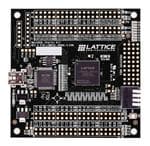


 工商网监
湘ICP备2023018690号
工商网监
湘ICP备2023018690号
