HDR-60 Base Board – Revision B
User’s Guide
April 2014
Revision: EB70_01.2
�HDR-60 Base Board – Revision B
Introduction
The HDR-60 Base Board provides a low-cost evaluation and demonstration platform to evaluate, test and debug
image signal processing user designs or IP, including High Dynamic Range (HDR) cores targeted for the
LatticeECP3™-70 FPGA. The HDR-60 Base Board and NanoVesta Head Board have been designed to work
together as part of the HDR-60 Video Camera Development Kit. Connections are available on the HDR-60 Base
Board for the A-1000 HDRI sensor from Aptina, scalable to future sensors from Aptina, and adaptable to sensors
from other manufacturers by redesigning the add-on NanoVesta Head Board. The HDR-60 Base Board features a
LatticeECP3-70 FPGA in the 484-ball fpBGA package. The LatticeECP3 I/Os are connected to a rich variety of
both generic and application-specific interfaces described later in this document.
Important: This document (including the schematics in Appendix A) describes the HDR-60 Base Board marked as
Revision B. This marking can be seen on the silkscreen of the printed circuit board, under the Lattice Semiconductor logo. The following are the changes from Revision A to Revision B.
• Added R136 and R137
• Installed R130 and R131
• Moved DVI_DDC_SCL signal to U2 pin D22
• Moved DVI_DDC_SDA signal to U2 pin G19
• Moved DVI_HPD signal to U2 pin C22
The LatticeECP3 is a third-generation device utilizing reconfigurable SRAM logic technology optimized to deliver
high-performance features such as an enhanced DSP architecture, high-speed SERDES and high-speed source
synchronous interfaces in an economical FPGA fabric. The LatticeECP3 devices also provide popular building
blocks such as LUT-based logic, distributed and embedded memory, Phase Locked Loops (PLLs), Delay Locked
Loops (DLLs), and advanced configuration support, including encryption, multi-boot capabilities and TransFR™
field upgrade features. The LatticeECP3 SERDES dedicated PCS functions, high jitter tolerance and low transmit
jitter allow the SERDES plus PCS blocks to be configured to support an array of popular data protocols including
PCI Express, SMPTE, Ethernet (XAUI, GbE, and SGMII), SATA I/II, OBSAI and CPRI. Transmit Pre-emphasis and
Receive Equalization settings make the SERDES suitable for transmission and reception over various forms of
media.
For a full description of the LatticeECP3 FPGA, including data sheet, technical notes and more, see the Lattice
web site at www.latticesemi.com/products/fpga/ecp3.
Some common uses for the HDR-60 Base Board include:
• Security/surveillance and automotive camera applications
• Evaluation of the Helion NanoVesta Head Board and other camera sensors
• Applications using Aptina Head Boards
• Evaluation of Helion IONOS Imaging Pipeline IP cores
• Ethernet IP camera applications
• Evaluation of Teradek H.264 compression modules
Features
Key features of the HDR-60 Base Board include:
• SPI serial Flash device included for low-cost, non-volatile configuration storage
• DDR2 SDRAM: 16-bit data over a 32M address space
• Tri-speed (10/100/1000 Mbit) Ethernet PHY with RJ-45 (includes 12 core magnetics)
2
�HDR-60 Base Board – Revision B
• Built-in USB 2.0 download to LatticeECP3
• Can be configured for a flywire ispDOWNLOAD™ cable connection
• HiSPi and parallel video data path connections with selectable VCCIO (1.8 V/2.5 V/3.3 V)
• Connectors for Aptina standard Head Board with USB 2.0 interface
• Connector for Teradek Capella H.264 codec board
• Test point connections to 19 I/O pins for prototyping
• Two MEMS and two crystal oscillators
• HDMI/DVI output using four channels (one quad) of differential SERDES
• 5.0 V, 3.3 V, 2.5 V, 1.8 V, 1.2 V voltages are generated from a single 12 V power source
• ispVM™ System programming support
General Description
The heart of the HDR-60 Base Board is the LatticeECP3 FPGA. The devices and connectors attached to the
LatticeECP3 provide a means to investigate applications developed for High Dynamic Range image signal processing. The board also provides several different interconnections and support devices that permit it to be used
for a variety of purposes. The HiSPi and parallel video input, DDR2 memory, Tri-speed Ethernet PHY, and HDMI
output are useful for applications using Lattice IP cores. A modest number of test points were added around the
board for general purpose LatticeECP3 I/O usage. The SPI memory showcases the fail-safe capabilities of the
LatticeECP3. Figure 1 is the block diagram for the HDR-60 Video Camera Development Kit.
Figure 1. HDR-60 Video Camera Development Kit Block Diagram
27 MHz
Teradek MPEG
Ethernet
Bank 6
Bank 7
25MHz
Bank 0
Aptina
Head Board
Refclk
Ch3
HDMI
Quad SERDES
Ch2
A
Ch1
LatticeECP3
-70EA
484 fpBGA
Ch0
Bank 1
Bank 3
Bank 2
NanoVesta
Head Board
DDR2 SDRAM
3
�HDR-60 Base Board – Revision B
Initial Setup and Handling
The following is recommended reading prior to removing the evaluation board from the static shielding bag and
may or may not apply to your particular use of the board.
CAUTION: The devices on the board can be damaged by improper handling.
The devices on the evaluation board contain fairly robust ESD (Electro Static Discharge) protection structures
within them, able to withstand typical static discharges (see the “Human Body Model” specification for an example
of ESD characterization requirements). Even so, the devices are static sensitive to conditions that exceed their
designed in protection. For example: higher static voltages, as well as lower voltages with lower series resistance
or larger capacitance than the respective ESD specifications can potentially damage or degrade the devices on the
evaluation board.
As such, it is recommended that you wear an approved and functioning grounded wrist strap at all times while handling the evaluation board when it is removed from the static shielding bag. If you will not be using the board for a
while, it is best to put it back in the static shielding bag. Please save the static shielding bag and packing box for
future storage of the board when it is not in use.
When reaching for the board, it is recommended that you first touch the ground plane of the board (for example, the
metal shielding of the HDMI connector). This will neutralize any static voltage difference between your body and the
board prior to any contact with signal I/O.
CAUTION: To minimize the possibility of ESD damage, the first and last electrical connections to the board should
always be from test equipment chassis ground to the ground plane of the board.
Before connecting signals or power to the board, attach a cable from chassis ground on grounded test equipment
to the ground plane of the board. Connecting the board ground to test equipment chassis ground will decrease the
risk of ESD damage to the I/O on the board as the initial connections to the board are made. Likewise, when
unplugging cables from the evaluation board, the last connection unplugged, should be the chassis GND connection to the evaluation board GND. If you have a signal source that is floating with respect to chassis GND, attempt
to neutralize any static charge on that signal source prior to attaching it to the evaluation board.
If you are holding or carrying the board when it is not in a static shielding bag, please keep one finger on the ground
plane of the board, for example the metal shielding of the HDMI connector. This will keep the board at the same
voltage potential as your body until you can pick up the static shielding bag and put the board back in it.
Electrical, Mechanical, and Environmental Specifications
The nominal board dimensions are 203.2 mm x 42 mm (8.000” x 1.654”). Additional mechanical board dimension
information is included on the mechanical drawing shown in Appendix A, Figure 24. On the physical board itself,
connectors include pin 1 indictors as either an arrow, or triangle point near pin 1 on the outer layer silk screen. The
environmental specifications are as follows:
• Operating temperature: 0 °C to 55 °C
• Storage temperature: -40 °C to 75 °C
• Humidity: Autoscan Options > Custom Scan as
shown in Figure 4.
15
�HDR-60 Base Board – Revision B
Figure 4. Setting the ispVM Custom Scan Option
5. Select Options > Cable and I/O Port Setup. For the Cable Type, select USB2, then click OK.
6. Push the Scan button. You should now see the LFE3-95/70 device listed in the New Scan Configuration Setup
window. In the device list, left-click on the LatticeECP3 device to select it. If offered other selections, select
LFE3-70EA. See Figure 5.
Figure 5. ispVM New Scan Configuration Setup
7. Click Edit > Edit Device to edit the device. A Device Information window will be opened. Click the Select button and select the package type 484-ball fpBGA as shown in Figure 6, then click OK.
Figure 6. LatticeECP3 Package Size Selection
8. Check that the Device Access Options drop-down menu control selects the JTAG 1532 Mode. Check that the
Operation drop-down menu selects Fast Program.
9. Click the data file Browse button and select the path to the LatticeECP3 “.BIT” bitstream file as shown in
Figure 7, then click OK.
16
�HDR-60 Base Board – Revision B
Figure 7. Bitstream Ready to Download into LatticeECP3 SRAM
10. Click Project >Download or the green Go button to download the bitstream into the LatticeECP3 device (U2).
A small window will appear as shown in Figure 8. It will take about 12 seconds to download the bitstream for a
PC with USB 2.0 ports. When the LatticeECP3 has loaded in correctly, the ispVM status window will report
“Operation Successful” as shown in Figure 9.
Figure 8. Bitstream Downloading into LatticeECP3
Figure 9. Bitstream Download Operation Successful
LatticeECP3 SRAM Configuration Using SPI Flash and USB Cable at J12
The LatticeECP3 SRAM can be configured easily using the ispVM System software to program the on-board SPI
Flash via a standard USB cable connected to the upper USB port at J12. The LatticeECP3 device is SRAM-based,
so it must remain powered on to retain its configuration when programming the SRAM. The on-board SPI Flash
retains its programmed bitstreams when power is off, and can quickly load programmed bitstreams into the
LatticeECP3 device when power is applied.
1. Attach a ground connection from test equipment chassis ground to the ground plane of the board, for example
on the metal HDMI connector.
17
�HDR-60 Base Board – Revision B
2. Connect the USB-A to USB-A cable from your PC’s USB connector to the upper USB port on J12 on the HDR60 Base Board.
3. Connect the 12 V wall power adaptor cable to J10 and check to see that the wall power adapter is plugged in to
a 120 VAC source.
4. Start the ispVM System software. Select the menu items Options > Autoscan Options > Custom Scan.
5. Select Options > Cable and I/O Port Setup. For the Cable Type, select USB2, then click OK.
6. Push the Scan button. You should now see the LFE3-95/70 device listed in the New Scan Configuration Setup
window. In the device list, left-click on the LatticeECP3 device to select it. If offered other selections, select
LFE3-70EA.
7. Click Edit > Edit Device to edit the device. A Device Information window will be opened. Click the Select button and select the package type 484-ball fpBGA, then click OK.
8. Click the Device Access Options drop-down menu control and select SPI Flash Background Programming.
A SPI Serial Flash Device window will open.
9. Push the Select button and select the Vendor as Numonyx, the device as SPI-M25P64 and the package 16lead SOIC as shown in Figure 10. Push the OK button.
Figure 10. SPI Flash Device Selection
10. Click the data file Browse button and select the path to the LatticeECP3 “.BIT” bitstream file. Push the Load
From File button and then click OK to complete the SPI Flash device selection as shown in Figure 11. Again
click OK to exit the Device Information menu. The bitstream is now set up for downloading into the SPI Flash
as shown in Figure 12.
18
�HDR-60 Base Board – Revision B
Figure 11. SPI Flash Device Setup Complete
Figure 12. Bitstream Ready to Download into SPI Flash
11. Click Project > Download or the green Go button to download the bitstream into the SPI Flash device (U9),
the bitstream download progress indictor will pop up as shown in Figure 13. When using the built-in USB download cable, it will take about two minutes to erase, program and verify the bitstream loaded properly into the
SPI Flash for a PC with USB 2.0 ports. After the SPI Flash contents have been verified, the ispVM status window will report “Operation Successful” as shown in Figure 14.
Figure 13. Bitstream Download Progress Indicator
19
�HDR-60 Base Board – Revision B
Figure 14. SPI Flash Download Operation Successful
12. Unpower the HDR-60 Base Board for a few seconds then power it back up. The design will load into the
LatticeECP3 (U2) from the external SPI Flash (U9) in two seconds, and the “DONE” LED (LED3) will light up.
References
• HDR-60 Video Camera Development Kit web page
• DS1021, LatticeECP3 Family Data Sheet
• HB1009, LatticeECP3 Family Handbook
• QS010, HDR-60 Video Camera Development Kit QuickSTART Guide
• EB63, NanoVesta Head Board User’s Guide
• TN1177, LatticeECP3 sysIO Usage Guide
• TN1169, LatticeECP3 sysCONFIG Usage Guide
20
�HDR-60 Base Board – Revision B
Ordering Information
Description
Ordering Part Number
China RoHS Environment-Friendly
Use Period (EFUP)
HDR-60 Video Camera Development Kit
(Contains: HDR-60 Base Board with LatticeECP3
FPGA pre-loaded with Image Signal Processing (ISP)
Demo, NanoVesta Head Board with Aptina A-1000
LFE3-70EAHDR60-DKN
720p HDR Sensor and Sunex lens, two USB cables,
HDMI cable with HDMI-to-DVI adapter, 12 V AC
adapter power supply, QuickSTART Guide)
HDR-60 Video Camera Base Board
(Contains: HDR-60 Base Board with LatticeECP3
FPGA pre-loaded with Image Signal Processing (ISP)
Demo, two USB cables, HDMI cable with HDMI-to-DVI
LFE3-70EAHDR60-EVN
adapter, 12 V AC adapter power supply, QuickSTART
Guide)
Note: Does not include NanoVesta Head Board.
Technical Support Assistance
e-mail:
techsupport@latticesemi.com
Internet: www.latticesemi.com
Revision History
Date
Version
Change Summary
August 2012
01.0
Initial release.
March 2013
01.1
Added HDR-60 Video Camera Base Board in Ordering Information.
April 2014
01.2
Updated references to BNC connector (J11) and Delta filter (U8) to indicate these are unpopulated on most boards. Ethernet-over-BNC is an
unsupported feature of this board.
Updated Technical Support Assistance information.
© 2014 Lattice Semiconductor Corp. All Lattice trademarks, registered trademarks, patents, and disclaimers are as
listed at www.latticesemi.com/legal. All other brand or product names are trademarks or registered trademarks of
their respective holders. The specifications and information herein are subject to change without notice.
21
�22
A
B
C
D
5
(Sheet 9)
Teradek MPEG
Encoder, USB
(Sheet 4)
1000Base-T
PHY/RJ45
HDR-60 Base Board Block Diagram
5
A
1
4
4
(Sheet 9)
Bank6
(Sheet 5)
DVI
Quad
A
(Sheet 5)
SerDes
3
(Sheet 7)
Bank3
Bank2
(Sheet 4)
Lattice
ECP3-70
484 ball
Bank7
(Sheet 4)
(Sheet 6)
Bank8
Bank1
(Sheet 8)
Bank0
(Sheet 8)
(Sheet 8)
(Sheet 8)
(top view)
Nanovesta
Head Board
Aptina
Head Board
3
(Sheet 7)
2
(Sheet 2, 3)
Voltage
Regulators
DDR2 16 Bit
(Sheet 4)
Nanovesta
Head Board
(Sheet 6)
Built In USB
2.0 Download
Programming
2
Date:
Size
C
Title
1
Wednesday, September 21, 2011
Sheet
1
HDR-60 Base Board Schematic
Project
Block Diagram
of
10
B
Rev
Lattice Semiconductor Corporation
5555 N.E. Moore Court
Hillsboro, Oregon. 97124
Rev B, 484 ball, -70
1
A
B
C
D
HDR-60 Base Board – Revision B
Appendix A. Schematic
Figure 15. Block Diagram
�A
B
C
1uF
EN
VIN
1
54_9K
22pF
5
1_2V, +1.2 V, 1A
SW
EN
4
VCC_CORE, +1.2 V, 1.35 A
1_8V, +1.8 V, 1.1 A
SW
3_3V, +3.3 V, 1.35 A
LDO
EN
PP7
5_0V, +5.0 V, 1.2 A
22uF
C210
NV_VDD, +1.8v/+2.5v/+3.3v, 1.1 A
SW
EN
5_0v
+5.0 v
1.2 A
SW
EN
SW
10ms RC
Power Supply Block Diagram
10_0K
R122
R123
C207
CDRH4D15/SNP-2R2NC
MBRM130LT3G
L5
2.2uH
D9
0.1uF
C205
D10 CMDSH-4E
2
Vout = 0.78*(R123/R122+1) = 5.06v
FB
SW
4
1
Ramp voltage at EN pin provides soft start
0.1uF
C209
6
100K
5
R124
U15
LT3503EDCB#PBF
C206
(5A fused)
12_0V
63V
10uF
C208
+
12_0V
1
2
D
1
2
3
GND
BOOST
PAD_GND
2
7
1
2
Voltage Regulators
C76
HEADER 3
J4
R51
D3
DFLS220L
L3
4.7uH
C77
22uF,6.3V
Male Power Jack 2.1mm
3
PJ-032A
3
POWER INPUT
+11v to +18v
3_3V
2
R42
51k
C64
R52
10_0K
J10
C81
F1251CT-ND
F1
R47
51k
C70
24
2
1
8
7
22
23
R48
63.4k
12_0V
C68
C78
D8
1N4448W
R43
34k
22
23
24
2
C5
10uF,25V
5A Fast-Blo SMT Socketed Fuse
12_0VIN
1
3_3V
C66
C69
1
8
7
C80
10uF,25V
D5
1N4448W
Vout = 0.8*(R53/R5+1) = 2.52 v
22_1K-0603SMT
Vout = 0.8*(R54/R52+1) = 1.21 v
PP4
C73
R56
R5
8_06K-0603SMT10_0K
R53
21_5K
D2
DFLS220L
L1
6.8uH
R54
5_11K
22uF,6.3V
C85
VCC_CORE
22uF,6.3V
C82
+1.2 v
1.35 A 1.2v/ms
Short 2-3: 3.298v
PP2
1
2
3
1.2v/ms
22uF,6.3V
Short 1-2: 1.806v
22uF,6.3V
C79
NV_VDD
+2.5 v
1.1 A
3
1
2
2
4
1
2
1
2
1
2
R44
51k
2
RT/SYNC
PG1
VC1
TRACK/SS1
FB1
SW1
BOOST1
21
R50
51k
RT/SYNC
PG1
VC1
TRACK/SS1
FB1
SW1
BOOST1
SHDN
1
2
1
21
SHDN
GND1
GND2
GND3
GND4
2
9
VIN1
GND5
25
9
VIN1
3
4
5
6
GND1
GND2
GND3
GND4
3
4
5
6
GND5
25
11
20
19
17
18
Date:
Size
B
Title
PG2
VC2
TRACK/SS2
FB2
SW2
BOOST2
C63
C75
C71
D6
1N4448W
C67
D7
1N4448W
3_3V
R45
11.5k
R46
35.7k
PP1
D1
DFLS220L
3_3V
R6
10k
1.2v/ms
R55
12.4k
PP3
D4
DFLS220L
L2
6.8uH
C8
22uF,6.3V
C4
22uF,6.3V
1_8v
C84
22uF,6.3V
C7
22uF,6.3V
+1.8v
1.1 A
3_3v
+3.3 v
1.35 A
Wednesday, September 21, 2011
1
Sheet
2
of
10
B
Rev
Lattice Semiconductor Corporation
5555 N.E. Moore Court
Hillsboro, Oregon. 97124
Vout = 0.8*(R55/R6+1) = 1.79 v
R49
51k
C72
C83
HDR-60 Base Board Schematic
Project
1.2v/ms
L4
4.7uH
1
Vout = 0.8*(R46/R45+1) = 3.28 v
R41
51k
C65
C74
Voltage Regulators
20
19
17
18
11
12
U11
LT3508EUF
12_0V
PG2
VC2
TRACK/SS2
FB2
SW2
BOOST2
12
U10
LT3508EUF
12_0V
10
VIN2
GND6
GND7
GND8
GND9
13
14
15
16
2
1
2
1
10
1
2
1
2
VIN2
GND6
GND7
GND8
GND9
13
14
15
16
1
2
1
23
2
5
A
B
C
D
HDR-60 Base Board – Revision B
Figure 16. Voltage Regulators
�A
B
C
1
16
BYP1
ADJ1
VOUT1
VOUT1_3
EN
U4
5
8
9
7
6
10
COUT1
10uF
10uF
6.3V
0805
COUT2
R13
L11
M10
E8
U17
U14
N13
AB16
N21
G11
K10
C19
T13
K11
P18
AA11
V7
M3
L10
V9
H15
F6
L13
F17
1
2
3
4
5
6
7
8
9
10
11
12
13
14
15
16
17
18
19
20
21
22
23
24
+1.2 v
500 mA
FB1
PP6
BLM41PG600SN1
FB4
BLM41PG600SN1
+ C182
+ C178
+ C179
C41
C46
C42
GND
ECP3_70EA_BGA484
U2L
GND
4
73
72
71
70
69
68
67
66
65
64
63
62
61
60
59
58
57
56
55
54
53
52
51
50
XRES
N15
F2
U10
E14
N10
H8
AB22
W16
R5
M12
H18
AA16
V14
Y16
AA12
C11
E21
P2
T12
AA9
V15
M7
W20
M11
H10
302 mA max
VCCA
100 mA max
R90
10k1%
C153
C145
C131
PCSA_VCCOB
28 mA max
PCSA_VCCIB
C126
C47
C158
C147
C177
C165
3
TP23
TP24
VCC_CORE
C142
C163
C160
TP25
TP26
+ C154
3_3V
FB10
BLM41PG600SN1 C113
3_3V
C156
C146
100NF-0402SMT
C137
100NF-0402SMT
1NF-0402SMT
FB2
BLM41PG600SN1
100NF-0402SMT
10NF-0402SMT
1_2v
+1.2 v
500 mA
PP5
1
2
0.46 v drop at 500 mA max
2.3v minimum input voltage
0.01uF
CBYP2
CIN2
1uF
25V
0805
LT3029EDE
BYP2
ADJ2
VOUT2
VOUT2_6
EN2
3_3v
ECP3 Symbol Pins:
* True LVDS Output
^ DQS
Density shown as -70
0.01uF
CBYP1
4
3
15
3_3v
14
13
VIN1
VIN1_13
12
11
VIN2
VIN2_11
NC
GND
GND_PAD
2
5
17
CIN1
1uF
25V
0805
1
2
GND
22UF-16V-TANTBSMT
22UF-16V-TANTBSMT
22UF-16V-TANTBSMT
1UF-16V-0805SMT
1UF-16V-0805SMT
1UF-16V-0805SMT
100NF-0402SMT
100NF-0402SMT
100NF-0402SMT
2
C168
+
2
C161
C134
C162
C128
C133
C155
C136
C143
C25
C139
C159
C152
100NF-0402SMT
10NF-0402SMT
D
1UF-16V-0805SMT
Core Power
3
C144
100NF-0402SMT
1NF-0402SMT
22UF-16V-TANTBSMT
100NF-0402SMT
1NF-0402SMT
1UF-16V-0805SMT
Date:
Size
B
Title
C170
100NF-0402SMT
4
22UF-16V-TANTBSMT
10NF-0402SMT
10NF-0402SMT
100NF-0402SMT
10NF-0402SMT
10NF-0402SMT
10NF-0402SMT
10NF-0402SMT
10NF-0402SMT
N11
K13
B9
G12
V2
K8
M16
Y4
N12
AA7
U13
AA10
AA15
D3
M13
AB1
AA13
T10
U9
L12
AA18
K12
R10
K2
Y7
98
97
96
95
94
93
92
91
90
89
88
87
86
85
84
83
82
81
80
79
78
77
76
75
74
10NF-0402SMT
1NF-0402SMT
VCCA
10NF-0402SMT
ECP3_70EA_BGA484
VCCAUX_M8
VCCAUX_R11
VCCAUX_H11
VCCAUX_M15
VCCAUX_R12
VCCAUX_H12
VCCAUX_L8
VCCAUX_L15
VCCA_V10
VCCA_V13
VCCA_U12
VCCA_U11
U2K
ECP3_70EA_BGA484
VCCPLL_L_K9
VCCPLL_L_N9
VCCPLL_R_K14
VCCPLL_R_N14
U2M
ECP3_70EA_BGA484
1
2
3
4
5
6
7
8
9
10
11
12
13
14
15
16
U2J
1
Wednesday, September 21, 2011
1
Sheet
3
HDR-60 Base Board Schematic
Project
M8
R11
H11
M15
R12
H12
L8
L15
V10
V13
U12
U11
K9
N9
K14
N14
J11
J9
P11
P12
J14
J13
M14
M9
P9
L9
P14
P10
J12
J10
L14
P13
VCC
of
10
B
Rev
Lattice Semiconductor Corporation
5555 N.E. Moore Court
Hillsboro, Oregon. 97124
VCCPLL
C149
C141
C129
10NF-0402SMT
Core Power
C148
10NF-0402SMT
1NF-0402SMT
1NF-0402SMT
1NF-0402SMT
25
26
27
28
29
30
31
32
33
34
35
36
37
38
39
40
41
42
43
44
45
46
47
48
49
24
T11
R8
B17
A1
R15
AA14
V8
P16
U6
N8
U21
J21
K15
L20
H13
L16
A22
J5
V16
W7
AA8
B13
B5
AB7
L7
10NF-0402SMT
5
A
B
C
D
HDR-60 Base Board – Revision B
Figure 17. Core Power
GND
�A
BANK 7
5
ECP3 Symbol Pins:
* True LVDS Output
^ DQS
Density shown as -70
TP2
TP1
R96
4_7K
R0402
C173
1uF
C0603
C26
3_3V
4_7K
C200
1uF, X5R, 6.3V
R119
4
1
2
GTXCLK
VCC
OUT
4
3
D7
D6
F10
D8
E10
F1
F2
33
3_3V
P_25MHz
3
100 FBGA
REGOUT
C181 C44
50 ohm ODT
10uF/6V3/X7R
F5
E4
n.c.
H4
B1
PHY_LOWPWR
RESETN
125MHz
LED1
LED2
LED3
LED4
n.c.
PHY_A0
PHY_A1
PHY_A2
PHY_A3
PHY_A4
G7
G6
H6
G10
A3
A4
C1
E6
E7
E8
E9
F6
F7
F8
F9
G2
G4
G5
H2
H3
H7
H10
J10
J9
K10
K9
K1
K2
K4
K3
K5
K6
K8
K7
R0402
R35
R0603 R32
R0603 R31
R29
DNI
R0603
Ferrites are all 0.45 ohm, 200ma, 0603
R100 DNI
R0603
R19
GMII default
4_7K
R0603
150
150
150
0R
0R
13
15
11
9
10
7
8
4
5
2
3
TP1+
TP1CT1
NC4
LED2_GRN_K
LED2_ORN_K
LED1_YEL_K
TRD4+
TRD4-
TRD3+
TRD3-
TRD2+
TRD2-
TRD1+
TRD1-
R24
DNI
R0402
R105
4_7K
R0402
R107
4_7K
R0603
R25
DNI
R0402
R21
DNI
R0603
R23
4_7K
R0402
3_3V
2
All high speed signals use 50 ohm traces
Date:
Size
B
Title
12
14
3_3V
C48
XTALVDD
C185 C186
AVDDL
PLLVDD
C183 C45
C184
Wednesday, September 21, 2011
1
Sheet
4
HDR-60 Base Board Schematic
of
10
B
Rev
Lattice Semiconductor Corporation
5555 N.E. Moore Court
Hillsboro, Oregon. 97124
2
FB16
Z-600 ohm / 74279265
1000Base-T PHY/RJ45
Project
2
3
4
100NF-0603SMT
C215
2
FB14
Z-600 ohm / 74279265
REGOUT 1
J11
1
BNC
LED3
1
1
2
FB5
Z-600 ohm / 74279265
REGOUT 1
AVDD
LED1_A
LED2_A
J12A
LED[1..4] powers up to: 1101 to set for
auto-negotiate, full duplex, 10/100/1000Base-T
R22
DNI
R0402
R103
4_7K
R0402
LED3 = Activity (Yellow ON)
8
7
6
5
C54
100NF-0603SMT
MTP1+
MTP1NC6
NC5
U8
LFB0001-R
0862-1J1T-43-F
1
2
3
4
LED[21] = Link speed
00: 1000Base-T (Orange & Green ON)
01: 100Base-T (Orange ON)
10: 10Base-T (Green ON)
11: no link
LED1 R0402 R33
LED2 R0402 R34
R30
DNI
R0603
100NF-0603SMT
C201
TDR0_P0
TDR0_M0
TRD outputs are all 100 ohm matched length diff pairs to
RJ45 connector. Place TDR(0) resistor common ends together.
2
PHY should power down when not in use
LOWPWR
NRESET
TVCOI
CLK125
LED[1]
LED[2]
LED[3]
LED[4]
NC3
NC4
NC21
NC46
NC47
NC48
NC49
NC56
NC57
NC58
NC59
NC62
NC64
NC65
NC72
NC73
NC77
PHYA[0]
PHYA[1]
PHYA[2]
PHYA[3]
PHYA[4]
TRD[0]+
TRD[0]TRD[1]+
TRD[1]TRD[2]+
TRD[2]TRD[3]+
TRD[3]-
3_3V
C180
+1.2v
DVDD
Z-600 ohm / 74279265
Z-600 ohm / 74279265
1
2
1
2
C43
FB3
FB13
100NF-0603SMT
3
BCM54810
R18
1_24K
R0402
Place resistor near osc
Place osc near U3
R0402 R115
TCK
TDI
TDO
TMS
NTRST
XTALI
XTALO
MDIO
MDC
GTXCLK
CRS
COL
TXC
TX_EN
TX_ER
TXD[0]
TXD[1]
TXD[2]
TXD[3]
TXD[4]
TXD[5]
TXD[6]
TXD[7]
RXC
RX_DV
RX_ER
RXD[0]
RXD[1]
RXD[2]
RXD[3]
RXD[4]
RXD[5]
RXD[6]
RXD[7]
DSC1001-CE-25.000
DI
DSC1001-CE-25-000
EN
GND
Y4
R20
1_24K
R0402
n.c.
P_25MHz
F4
E3
A7
E5
D5
4_7K
C6
CRS
COL
A8
TXC
A9
TX_EN
A2
TX_ER
RXC
C7
C8
B6
B7
B8
B9
B10
A10
R0402 R99
MDIO
MDC
BLM21AG601SN1D
A1
B2
RX_ER
RX_DV
TXD0
TXD1
TXD2
TXD3
TXD4
TXD5
TXD6
TXD7
SW PUSHBUTTON-SPST
SW1
GSRN
R16
301K
R0402
D4
D3
C3
C4
C5
B5
B4
B3
RXD0
RXD1
RXD2
RXD3
RXD4
RXD5
RXD6
RXD7
U3
C199
0.1uF
FB20
3_3V
C50
6
5
2
FB17
Z-600 ohm / 74279265
1
100NF-0603SMT
Z-600 ohm / 74279265
1
2
REGSUPPLY
FB15
C49 C187
BIASVDD
C51
AVDDL
PLLVDD
XTALVDD
100NF-0603SMT
741X083472JP
8
3_3V
7
4_7K
R0402
4_7K
R17
100R
R0402
R98
RN4
1
2
3
4
AVDD
C194
3_3V
10uF/6V3/X7R
4
100NF-0603SMT
C52
33uF/6V3
TX and RX traces are all matched length
125MHz
RX_DV
RXC
RXD1
RXD0
TXC
3_3V
C114
C31
C112
C151
C167
3_3V
C169
ECP3_70EA_BGA484
1NF-0402SMT
J8
K7
L6
MDIO
1NF-0402SMT
VCCIO7_J8
VCCIO7_K7
VTT7
1
ECP3_GSRN
TP5
TP6
PHY_LOWPWR
MDC
TXD5
TXD6
TXD4
TX_EN
TXD0
TXD3
TXD7
TXD2
TXD1
TX_ER
RXD5
CRS
RESETN
RXD7
RXD2
RXD4
COL
RXD6
RXD3
RX_ER
GTXCLK
PHY_A0
PHY_A1
PHY_A2
PHY_A3
PHY_A4
10NF-0402SMT
B
E3
D4
E5
E4
B2
C2
F5
F4
D2
D1
G4
G5
E2
F3
H4
J4
B1
C1
H5
H6
G3
G2
E1
F1
G1
H1
J7
J6
H2
H3
J3
K3
J2
J1
K4
K5
K1
L1
L5
K6
100NF-0603SMT
C
PL8A
PL8B
PL10A*
PL10B*
PL11A*
PL11B*
PL13A^
PL13B^
PL14A
PL14B
PL16A*
PL16B*
PL26A
PL26B
PL28A*
PL28B*
PL29A*
PL29B*
PL31A^
PL31B^
PL32A
PL32B
PL34A*/VREF1_7
PL34B*/VREF2_7
PL35A
PL35B
PL37A*/LUM0_GDLLT_IN_A
PL37B*/LUM0_GDLLT_IN_B
PL38A*/LUM0_GDLLT_FB_A
PL38B*/LUM0_GDLLT_FB_B
PL40A^
PL40B^
PL41A
PL41B
PL43A*/PCLKT7_0
PL43B*/PCLKC7_0
PL43E_A/LUM0_GPLLT_FB_A
PL43E_B/LUM0_GPLLT_FB_B
PL43E_C/LUM0_GPLLT_IN_A
PL43E_D/LUM0_GPLLT_IN_B
U2E
10NF-0402SMT
10uF/6V3/X7R
J1
D
100NF-0603SMT
10uF/6V3/X7R
C10
D1
D10
2
FB18
Z-600 ohm / 74279265
3_3V
10uF/6V3/X7R
G1
XTALVDD
E1
PLLVDD
J3
J4
AVDDL1
AVDDL2
J2
J8
AVDD1
AVDD2
GND1
GND2
GND3
GND4
GND5
GND6
GND7
C2
C9
D9
E2
J5
J6
J7
BIASVDD
H1
6
CT
1000Base-T PHY/RJ45
1
2
100NF-0603SMT
OVDD
OVDD_RGMII
F3
REGOUT
A6
A5
RDAC
RJ45 (1..8)
GND
1
G3
REGSUPPLY
RGMII_SEL[0]
RGMII_SEL[1]
H5
D2
10uF/6V3/X7R
10uF/6V3/X7R
10uF/6V3/X7R
DVDD1
DVDD2
DVDD3
TEST0
TEST1
TEST2
TEST3
H8
H9
G8
G9
100NF-0603SMT
100NF-0603SMT
25
100NF-0603SMT
5
A
B
C
D
HDR-60 Base Board – Revision B
Figure 18. 100Base-T PHY/RJ45
�A
B
C
DVI_DDC_SCL
DVI_HPD
DVI_DDC_SDA
100R
DNI
R132
100R
R131
R130
5
W15
W12
W11
W8
W14
W13
W10
W9
Y15
Y14
Y12
Y13
Y11
Y10
Y8
Y9
AB15
AB14
AB12
AB13
AB11
AB10
AB8
AB9
V12
V11
5_0V
ECP3_70EA_BGA484
SERDES
Quad A
PCSA_VCCIB0
PCSA_VCCIB1
PCSA_VCCIB2
PCSA_VCCIB3
PCSA_VCCOB0
PCSA_VCCOB1
PCSA_VCCOB2
PCSA_VCCOB3
ECP3 Symbol Pins:
* True LVDS Output
^ DQS
Density shown as -70
{6}
U2F
PCSA_HDINP0
PCSA_HDINN0
PCSA_HDINP1
PCSA_HDINN1
PCSA_HDINP2
PCSA_HDINN2
PCSA_HDINP3
PCSA_HDINN3
PCSA_HDOUTP0
PCSA_HDOUTN0
PCSA_HDOUTP1
PCSA_HDOUTN1
PCSA_HDOUTP2
PCSA_HDOUTN2
PCSA_HDOUTP3
PCSA_HDOUTN3
PCSA_REFCLKP
PCSA_REFCLKN
PCSA_VCCOB
PCSA_VCCIB
HPD
DDC_SCL
DDC_SDA
CEC_OUT
DVI_HDOUTP0
DVI_HDOUTN0
DVI_HDOUTP1
DVI_HDOUTN1
DVI_HDOUTP2
DVI_HDOUTN2
DVI_HDOUTP3
DVI_HDOUTN3
27K
D
4.7K
R135
DVI
4.7K
R134
26
R133
5
4
4
C219
1uF
C56
1uF
C220
1uF
C57
1uF
TMDSOUT_DATACLK-
TMDSOUT_DATACLK+
All high speed signals use 50 ohm traces
C221
1uF
C58
1uF
C218
1uF
C55
1uF
DVI signals are all matched length
3
3
TMDSOUT_DATA0+
TMDSOUT_DATA0-
NAME
NC
SCL
SDA
DDC/CEC GROUND
+5V POWER
15
16
17
18
TMDSOUT_DATA1-
TMDSOUT_DATA1+
2
TMDSOUT_DATA2-
TMDSOUT_DATA2+
HOT PLUG DETECT
CEC
14
19
TMDS CLOCK-
13
TMDS CLOCK SHIELD
11
12
TMDS CLOCK+
10
TMDS DATA0+
7
TMDS DATA0 SHIELD
TMDS DATA1-
6
TMDS DATA0-
TMDS DATA1 SHIELD
9
TMDS DATA1+
5
8
TMDS DATA2-
4
TMDS DATA2 SHIELD
TMDS DATA2+
3
2
1
PIN NO
2
Date:
Size
B
Title
J13
20
21
22
23
20
21
22
23
1M
100nF
Wednesday, September 21, 2011
1
Sheet
5
of
10
B
Rev
Lattice Semiconductor Corporation
5555 N.E. Moore Court
Hillsboro, Oregon. 97124
SHIELD
R36
C59
HDR-60 Base Board Schematic
Project
BLM41PG600SN1
5_0V
HDMI/DVI Output
10nF
C222
500254_1927
1
2
3
4
5
6
7
8
9
10
11
12
13
14
15
16
17
18
19
DVI
1
2
3
4
5
6
7
8
9
10
11
12
13
14
15
16
17
18
19
100nF
C60
FB21
1
A
B
C
D
HDR-60 Base Board – Revision B
Figure 19. DVI
�A
B
C
C61
100nF
C62
100nF
FLASH_DIS
5
ECP3 Symbol Pins:
* True LVDS Output
^ DQS
Density shown as -70
3_3V
R40
10k
3_3V
100nF
C53
5_0V
1
2
3
4
5
6
7
8
1
2
DI
M25P64
NHOLD
VCC
NC1
NC2
NC3
NC4
NS
Q
U9
5
6
ORG
C
D
NC8
NC7
NC6
NC5
VSS
NW
R38
10k
NW
R37
10k
USB1_Q
FPGA_MCLK
FPGA_SISPI
4
R39
10k
3_3V
USB1_SK
USB1_D
R126 27
R125 27
R110
1M
DI
USB1_CS
SPI0_Q
FPGA_CSSPI0N_DI
16
15
14
13
12
11
10
9
10k
DIN
QOUT
R116
VSS
3
U7
M93C46-WMN6TP
8
1
VCC
CS
7
2
CLK
N.C.
DI
R113 1K
0862-1J1T-43-F
VP
USBUSB+
GND
USB2_1
USB2_2
USB2_3
USB2_4
100nF
C195
12pF
6 MHz
12pF
DI
DI
ATS060SM-1 HC-49/US-SM
C189
Y2
(Upper USB, ispVM)
PROG
J12C
C216
4
C211
33pF
R137
1K
R27
1k5
R112
10k
100nF
EECS
EESK
EEDATA
TEST
XTOUT
XTIN
NOT_RSTOUT
USBDM
USBDP
NOT_RSTIN
3V3OUT
TXD_UART
RXD_UART
C37
C123
3_3V
DVI_DDC_SDA
SPI0_Q
FPGA_SISPI
3_3V
{5}
{5} DVI_HPD
DVI_DDC_SCL
FPGA_MCLK
FPGA_WRITEN
3
G16
H16
C18
B19
E18
E17
A20
B20
D18
D19
C21
D21
F19
F18
A21
B22
J16
H17
C22
D22
G17
G18
G19
G20
H19
H20
41
30
29
28
27
26
40
39
38
37
36
35
33
32
15
13
12
11
10
24
23
22
21
20
19
17
16
0R
0R
0R
0R
100nF
TXD_UART
RXD_UART
R106
R102
R104
R101
C188
3_3V
3
CFG0
CFG1
CFG2
BANK 8
ECP3_70EA_BGA484
VCCIO8_G16
VCCIO8_H16
PT140A
PT140B
PT142A
PT142B
PT143A
PT143B
PT145A
PT145B
H7
G7
G6
C3
C4
E20
E19
B21
F21
0R
R86
DONE
INITN
F20
PROGRAMN
D20
R11
2k2
3_3V
C20
USB_TCK
USB_TDI
USB_TDO
USB_TMS
PR5A
PR5B/DI/CSSPI0N/CSSPIN
PR7A/CS1N/HOLDN/CONT2N
PR7B/CSN/SN/CONT1N
PR8A/DOUT/CS0N/CSSPI1N
PR8B/MCLK
PR10A/WRITEN
PR10B/D0/SPIFASTN
PR11A/D1
PR11B/D2
PROGRAMN
PR13A/D3/SI
PR13B/D4/SO
INITN
PR14A/D5
PR14B/D6/SPID1
CCLK
PR16A/D7/SPID0
PR16B/BUSY/SISPI
DONE
U2G
NOT_PWREN
BCBUS0
BCBUS1
BCBUS2
BCBUS3
SI/WUB
BDBUS0
BDBUS1
BDBUS2
BDBUS3
BDBUS4
BDBUS5
BDBUS6
BDBUS7
ACBUS0
ACBUS1
ACBUS2
ACBUS3
SI/WUA
ADBUS0
ADBUS1
ADBUS2
ADBUS3
ADBUS4
ADBUS5
ADBUS6
ADBUS7
U5
FTD2232D
3_3V
TP15
FPGA_CSSPI0N_DI
FPGA_CS1N
FPGA_CSN
48
1
2
47
44
43
5
8
7
4
6
R109
330R 5_0V
C121
TP19
TP18
TP11
TP3
TP21
TP12
TP16
TP13
TP20
TP7
R65 R70 R71
4_7K 4_7K 4_7K
3_3V
2_2K
R136
DNI
R114
DI
C212
33pF
33nF
C190
100nF
C191
1NF-0402SMT
D
5_0V
C193
10NF-0402SMT
USB Download
4
46
AVCC
3
42
14
31
DVCC_3
DVCC_42
VCCIOA
VCCIOB
DGND_9
DGND_18
DGND_25
DGND_34
9
18
25
34
AGND
45
100NF-0603SMT
2
R12 10K
R10
2k2
1
R8
2k2
ECP3_70EA_BGA484
VCCJ
TCK
TDI
TDO
TMS
U2H
2
3_3V
LED2
LED3
green
Date:
Size
B
Title
VCC
NC
TCK
TMS
INITN GND
7
1
R13
R9
R7
DONE
INITN
PROGRAMN
1
Wednesday, September 21, 2011
1
Sheet
6
HDR-60 Base Board Schematic
Project
3_3V
100NF-0603SMT
of
10
B
Rev
Lattice Semiconductor Corporation
5555 N.E. Moore Court
Hillsboro, Oregon. 97124
2k2
2k2
3_3V
2k2
TMS
GND
TCK
DONE
INITn
+3.3V
TDO
TDI
PROGRAMn
HEADER 10
DNI
TDO
ispEN_N
TDI
DONE
J3
2
3
4
5
6
8
9
10
USB Download
LED1
red
R4
4_7k
red
R1
1_0k
Q1
MMBT3904
3_3V
R2
4_7k
R3
4_7k
3_3V
C6
100nF
3
27
2
C3
Local JTAG
header (ispVM)
5
A
B
C
D
HDR-60 Base Board – Revision B
Figure 20. USB Download
�A
B
C
100nf
C118
DDR2_VREF
DDR2_VTT
1k
1
5
LP2998
VREF
10nf
10nf
C110
8
5
6
7
100nF
BA0
BA1
A0
A1
A2
A3
A4
A5
A6
A7
A8
A9
A10/AP
A11
A12
47uF
+
C93
1_8V
IS43DR16320B
4
47uF
+ C13
DDR2_DM1
DDR2_DQ8
DDR2_DQ9
DDR2_DQ10
DDR2_DQ11
DDR2_DQ12
DDR2_DQ13
DDR2_DQ14
DDR2_DQ15
DDR2_DM0
DDR2_DQ0
DDR2_DQ1
DDR2_DQ2
DDR2_DQ3
DDR2_DQ4
DDR2_DQ5
DDR2_DQ6
DDR2_DQ7
F3
G8
G2
H7
H3
H1
H9
F1
F9
B3
C8
C2
D7
D3
D1
D9
B1
B9
DDR2_DQS1_P
DDR2_DQS1_N
DDR2_DQS0_P
DDR2_DQS0_N
DDR2_BA0
DDR2_BA1
DDR2_A0
DDR2_A1
DDR2_A2
DDR2_A3
DDR2_A4
DDR2_A5
DDR2_A6
DDR2_A7
DDR2_A8
DDR2_A9
DDR2_A10
DDR2_A11
DDR2_A12
DDR2_CSN
DDR2_RASN
DDR2_CASN
DDR2_WEN
DDR2_CK_N
DDR2_CK_P
DDR2_CKE
B7
A8
F7
E8
L2
L3
M8
M3
M7
N2
N8
N3
N7
P2
P8
P3
M2
P7
R2
L8
K7
L7
K3
K8
J8
K2
3_3V
100nF
C10
VSSQ_A7
UDQS
VSSQ_B2 NOT_UDQS
VSSQ_B8
LDQS
VSSQ_D2 NOT_LDQS
VSSQ_D8
VSSQ_E7
LDM
VSSQ_F2
DQ0
VSSQ_F8
DQ1
VSSQ_H2
DQ2
VSSQ_H8
DQ3
DQ4
DQ5
VDD_A1
DQ6
VDD_E1
DQ7
VDD_J9
VDD_M9
UDM
VDD_R1
DQ8
DQ9
DQ10
VSS_A3
DQ11
VSS_E3
DQ12
VSS_J3
DQ13
VSS_N1
DQ14
VSS_P9
DQ15
VDDQ_A9
VDDQ_C1
VDDQ_C3
VDDQ_C7
VDDQ_C9
VDDQ_E9
VDDQ_G1
VDDQ_G3
VDDQ_G7
VDDQ_G9
VDDL
VSSDL
NOT_CS
NOT_RAS
NOT_CAS
NOT_WE
N.C.1
N.C.2
N.C.3
N.C.4
N.C.5
N.C.6
DDR2_VTT
A3
E3
J3
N1
P9
A1
E1
J9
M9
R1
A7
B2
B8
D2
D8
E7
F2
F8
H2
H8
A9
C1
C3
C7
C9
E9
G1
G3
G7
G9
J1
J7
A2
E2
L1
R3
R7
R8
C15
DDR2_VTT
VDDQ
AVIN
PVIN
VTT
100nf
C108
100nf
C103
VSENSE
NSD
GND
U12
C117
4
3
2
C109
1uf
22uF / 6V3
ECP3 Symbol Pins:
* True LVDS Output
^ DQS
Density shown as -70
3_3V
R59
FB8
BLM41PG600SN1
1uf
C104
C102
1_8V
22uF / 6V3
C101
1_8V
100nf
1uf
22uF / 6V3
FB9
BLM41PG600SN1
C111
C115
FB11
BLM41PG600SN1
10nf
100nf
C116
1_8V
C106
C107
NOT_CLK
CLK
CKE
VREF
C23 100nF
D
J2
U1
C96 100nF
DDR2_VREF
C21 100nf
ODT
C94 100nF
K9
C99 100nF
DDR2_ODT
DNI
R64
F_27MHz
R91
49_9R
R0402
R88
40_2R
R0402
DDR2_CK_N
DDR2_CK_P
50R
50R
R60
R61
10nf
C105
Place resistors near U2
F_27MHz
C24 100nF
4
C18 100nF
DDR2 Memory
10nf
C20
10nf
C22
10nf
C97
10nf
C95
10nf
C16
10nf
C19
10nf
C17
10nf
C98
28
C100 100nF
5
3
3
47uF
C88
+
10nf
100nf
47uF
C89
+
C92
C12
N16
P15
M17
P22
R21
N19
M19
R22
T22
N18
P19
T20
R20
P20
N20
U22
V22
R16
P17
Y22
W22
T21
U20
Y21
W21
R19
R18
V21
V20
R17
T17
AA22
AB21
T19
T18
U19
U18
AA21
Y20
W19
V19
AA20
AB20
U16
U15
AB17
AA17
T14
R14
AB18
AB19
W18
W17
Y17
Y18
V18
V17
AA19
Y19
T15
T16
1_8V
1_8V
DDR2_VTT
DDR2_A12
DDR2_WEN
DDR2_BA1
DDR2_A4
DDR2_A11
DDR2_RASN
DDR2_A1
DDR2_A8
DDR2_A0
DDR2_A7
DDR2_A5
DDR2_A6
DDR2_BA0
DDR2_CASN
DDR2_A3
DDR2_CK_P
DDR2_CK_N
DDR2_A10
DDR2_CKE
DDR2_CSN
DDR2_A9
DDR2_A2
DDR2_DQ6_r
DDR2_DQ4_r
DDR2_DQ5_r
DDR2_DQ7_r
DDR2_DQ0_r
DDR2_DQ3_r
DDR2_DQS0_P_r
DDR2_DQS0_N_r
DDR2_DQ2_r
DDR2_DQ1_r
DDR2_VREF
DDR2_DM0_r
DDR2_DQ12_r
DDR2_DQ9_r
DDR2_DQ14_r
DDR2_DQ15_r
DDR2_DQ13_r
DDR2_DQ10_r
DDR2_DQS1_P_r
DDR2_DQS1_N_r
DDR2_DQ8_r
DDR2_DQ11_r
DDR2_ODT
DDR2_DM1_r
BANK 3
10nf
C11
2
Place DQS resistors
close to ECP3
All high speed signals use 50 ohm traces
100nf
C14
ECP3_70EA_BGA484
VCCIO3_N16
VCCIO3_P15
VTT3
PR44A
PR44B
PR46A*/PCLKT3_0
PR46B*/PCLKC3_0
PR47A*
PR47B*
PR49A^
PR49B^
PR50A
PR50B
PR52A*/VREF1_3
PR52B*/VREF2_3
PR53A
PR53B
PR55A*
PR55B*
PR56A*
PR56B*
PR58A^
PR58B^
PR59A
PR59B
PR61A*
PR61B*
PR61E_A/RLM1_GPLLT_FB_A
PR61E_B/RLM1_GPLLT_FB_B
PR61E_C/RLM1_GPLLT_IN_A
PR61E_D/RLM1_GPLLT_IN_B
PR89A
PR89B
PR91A*
PR91B*
PR92A*
PR92B*
PR94A^
PR94B^
PR95A
PR95B
PR97A*
PR97B*
PB133A
PB133B
PB134A
PB134B
PB136A
PB136B
PB137A
PB137B
PB139A
PB139B
PB140A
PB140B
PB142A
PB142B
PB143A
PB143B
PB145A
PB145B
U2I
2
R85
R81
R75
R76
R14
R15
R74
R68
R77
R69
R63
R72
R66
R67
R78
R62
R73
R84
Date:
DDR2 Memory
RN2
1
2
3
4
5
6
7
8
33R
33R
33R
33R
33R
33R
33R
33R
33R
33R
33R
33R
33R
33R
33R
33R
33R
33R
33R
33R
33R
33R
DDR2_DQS1_P_r
DDR2_DQS1_N_r
DDR2_DQS0_P_r
DDR2_DQS0_N_r
DDR2_DM0_r
DDR2_DM1_r
DDR2_DQ0_r
DDR2_DQ1_r
DDR2_DQ2_r
DDR2_DQ3_r
DDR2_DQ4_r
DDR2_DQ5_r
DDR2_DQ6_r
DDR2_DQ7_r
DDR2_DQ8_r
DDR2_DQ9_r
DDR2_DQ10_r
DDR2_DQ11_r
DDR2_DQ12_r
DDR2_DQ13_r
DDR2_DQ14_r
DDR2_DQ15_r
DDR2_VTT
DDR2_VTT
Wednesday, September 21, 2011
1
Sheet
7
HDR-60 Base Board Schematic
Project
1
2
3
4
5
6
7
8
DDR2_VTT
of
10
B
Rev
Lattice Semiconductor Corporation
5555 N.E. Moore Court
Hillsboro, Oregon. 97124
R83
R82
Size
B
RN3
100 OHM ARRAY
DI
16
15
14
13
12
11
10
9
DDR2_DQS1_P R0402
DDR2_DQS1_N R0402
Title
1
2
3
4
5
6
7
8
100 OHM ARRAY
DI
16
15
14
13
12
11
10
9
R79
R80
R0402
R0402
DDR2_DM0
DDR2_DM1
RN1
100 OHM ARRAY
DI
16
15
14
13
12
11
10
9
DDR2_DQS0_P R0402
DDR2_DQS0_N R0402
R0402
R0402
R0402
R0402
R0402
R0402
R0402
R0402
R0402
R0402
R0402
R0402
R0402
R0402
R0402
R0402
DDR2_DQ0
DDR2_DQ1
DDR2_DQ2
DDR2_DQ3
DDR2_DQ4
DDR2_DQ5
DDR2_DQ6
DDR2_DQ7
DDR2_DQ8
DDR2_DQ9
DDR2_DQ10
DDR2_DQ11
DDR2_DQ12
DDR2_DQ13
DDR2_DQ14
DDR2_DQ15
DDR2_ODT
DDR2_CASN
DDR2_CKE
DDR2_BA1
DDR2_BA0
DDR2_A10
DDR2_A7
DDR2_A11
DDR2_A8
DDR2_A12
DDR2_WEN
DDR2_CSN
DDR2_RASN
DDR2_A0
DDR2_A1
DDR2_A2
DDR2_A3
DDR2_A4
DDR2_A5
DDR2_A9
DDR2_A6
1
A
B
C
D
HDR-60 Base Board – Revision B
Figure 21. DDR2 Memory
C9 100nF
�A
B
C
C1
5_0V
SLVS_11N
SLVS_11P
SLVS_10N
SLVS_10P
5_0V
C2
5_0V
ECP3 Symbol Pins:
* True LVDS Output
^ DQS
Density shown as -70
5_0V
5
SLVS_0N
SLVS_0P
SLVS_6N
SLVS_6P
SLVS_2N
SLVS_2P
SLVS_7N
SLVS_7P
SLVS_1N
SLVS_1P
5_0V
5_0V
EXTCLK_FPGA
LINE_VALID
DOUT6
DOUT2
DOUT7
DOUT3
DOUT10
DOUT11
TRIGGER
RESET_BAR
OUTPUT_EN_BAR
STANDBY
1NF-0402SMT
SHIELD2
1
3
5
7
9
11
13
15
17
19
21
23
25
27
29
31
33
35
37
39
SHIELD1
PIN2
PIN4
PIN6
PIN8
PIN10
PIN12
PIN14
PIN16
PIN18
PIN20
PIN22
PIN24
PIN26
PIN28
PIN30
PIN32
PIN34
PIN36
PIN38
PIN40
2
4
6
8
10
12
14
16
18
20
22
24
26
28
30
32
34
36
38
40
R93
R87
R92
STANDBY
RESET_BAR
SADDR
2
4
6
8
10
12
14
16
18
20
22
24
26
28
30
32
34
36
38
40
100_R
100_R
100_R
100_R
TP4
SLVS_8N
SLVS_8P
SLVS_9N
SLVS_9P
TP8
TP10
TP17
DOUT9
TRIGGER
OUTPUT_EN_BAR
DOUT4
5_0V
TP22
HISPI_RESETN
HISPI_LED
SLVS_4N
SLVS_4P
SLVS_CN
SLVS_CP
SLVS_5N
SLVS_5P
SLVS_3N
SLVS_3P
RESERVED_1
HISPI_SDATA
HISPI_SCLK
VDDIO_rH
5_0V
DF12__-40DS-0.5V_RECEPTACLE
SHIELD_2
PIN2
PIN4
PIN6
PIN8
PIN10
PIN12
PIN14
PIN16
PIN18
PIN20
PIN22
PIN24
PIN26
PIN28
PIN30
PIN32
PIN34
PIN36
PIN38
PIN40
HiSPI
PIN1
PIN3
PIN5
PIN7
PIN9
PIN11
PIN13
PIN15
PIN17
PIN19
PIN21
PIN23
PIN25
PIN27
PIN29
PIN31
PIN33
PIN35
PIN37
PIN39
DNI
DNI
DNI
DNI
5_0V
PIXCLK
FRAME_VALID
DOUT4
DOUT0
DOUT5
DOUT1
DOUT8
DOUT9
SADDR
SCLK
SDATA
OSC_ENABLE
VDDIO_rP
4
VCCIO1_G13
VCCIO1_H14
SLVS_11P
SLVS_11N
SLVS_10P
SLVS_10N
SLVS_9P
SLVS_9N
SLVS_8P
SLVS_8N
SLVS_7P
SLVS_7N
SLVS_6P
SLVS_6N
HISPI_SDATA
RESERVED_1
SLVS_5P
SLVS_5N
SLVS_0P
SLVS_0N
SLVS_4P
SLVS_4N
SLVS_1P
SLVS_1N
SLVS_CP
SLVS_CN
SLVS_2P
SLVS_2N
SLVS_3P
SLVS_3N
BANK 2
3
3_3V
5_0V
3
All high speed signals use 50 ohm traces
C29
C32
C34
C30
C33
C127
ECP3_70EA_BGA484
VCCIO2_15
VCCIO2_K16
VTT2
PR26A
PR26B
PR28A*
PR28B*
PR29A*
PR29B*
PR31A^
PR31B^
PR32A
PR32B
PR34A*/VREF1_2
PR34B*/VREF2_2
PR35A
PR35B
PR37A*/RUM0_GDLLT_IN_A
PR37B*/RUM0_GDLLT_IN_B
PR38A*/RUM0_GDLLT_FB_A
PR38B*/RUM0_GDLLT_FB_B
PR40A^
PR40B^
PR41A
PR41B
PR43A*/PCLKT2_0
PR43B*/PCLKC2_0
PR43E_A/RUM0_GPLLT_FB_A
PR43E_B/RUM0_GPLLT_FB_B
PR43E_C/RUM0_GPLLT_IN_A
PR43E_D/RUM0_GPLLT_IN_B
U2C
C35
C135
NV_VDD
NV_VDD
J15
K16
L17
E22
F22
J17
J18
G21
G22
J19
J20
H21
H22
K17
K18
J22
K22
K20
K19
K21
L21
L18
L19
L22
M22
M21
M20
P21
N22
M18
N17
C132
C125
C36
C120
BANK 1
ECP3_70EA_BGA484
C138
G13
H14
PT74A
PT74B
PT76A/PCLKT1_0
PT76B/PCLKC1_0
PT77A
PT77B
PT79A^
PT79B^
PT80A
PT80B
PT82A
PT82B
PT83A
PT83B
PT85A
PT85B
PT86A
PT86B
PT88A^
PT88B^
PT89A
PT89B
PT91A
PT91B
PT128A
PT128B
PT130A
PT130B
PT131A
PT131B
PT133A^
PT133B^
PT134A
PT134B
PT136A/VREF1_1
PT136B/VREF2_1
U2B
C122
NV_VDD
NV_VDD
B11
B12
C12
PIXCLK
D12
A12
VDDIO_rP
A13
VDDIO_rH
E12
E13
C13
HISPI_RESETN
C14
HISPI_SCLK
D13
D14
A14
B14
F13
F14
R94
0402 33_R A15
B15
E16
E15
OSC_ENABLE
C15
SDATA
D15
SCLK
G15
SADDR
G14
DOUT9
A16
DOUT4
B16
FRAME_VALID
F15
STANDBY
OUTPUT_EN_BAR F16
A17
RESET_BAR
B18
TRIGGER
C17
DOUT11
C16
DOUT6
A18
LINE_VALID
A19
EXTCLK_FPGA
D16
D17
U2-J22 and U2-K22 are routed
as a matched length diff pair
Place 100 ohm resistors as close as possible to ECP3 pins
R89
5_0V
FRAME_VALID
DF12(4.0)-40DP-0.5V_HEADER
SHIELD_2
PIN1
PIN3
PIN5
PIN7
PIN9
PIN11
PIN13
PIN15
PIN17
PIN19
PIN21
PIN23
PIN25
PIN27
PIN29
PIN31
PIN33
PIN35
PIN37
PIN39
SHIELD_1
SHIELD_1
J1
SHIELD2
1
3
5
7
9
11
13
15
17
19
21
23
25
27
29
31
33
35
37
39
SHIELD1
Parallel
1NF-0402SMT
1NF-0402SMT
J2
4
1NF-0402SMT
1NF-0402SMT
5
10NF-0402SMT
D
1NF-0402SMT
10NF-0402SMT
10NF-0402SMT
{9} CYP_SDA
{9} CYP_SCL
BLM41PG600SN1
FB7
BLM41PG600SN1
FB6
C87
100nF
R58
4_7K
C90
100nF
R57
4_7K
ECP3_SHIP_DATA
HEAD_SHIP_DATA
CYP_SDA
3_3V
ECP3_SHIP_CLK
HEAD_SHIP_CLK
CYP_SCL
3_3V
C91
100nF
Aptina
2
4
6
8
10
12
14
16
18
20
22
24
26
J6
J5
HEADER 3
1
2
3
HEADER 3
1
2
3
100nF
1
2
3
4
5
6
7
8
9
10
11
12
13
J8
HEAD_MCLK
HEAD_SP5
HEAD_SENSOR_RESETN
HEAD_SHIP_DATA
HEAD_SP6
HEAD_DOUT1
HEAD_DOUT3
HEAD_DOUT5
HEAD_DOUT7
HEAD_DOUT9
2
PINHD-1X13-FEMALE-ROUND
1
2
3
4
5
6
7
8
9
10
11
12
13
C86
PINHD-2X13-FEMALE-ROUND
1
3
5
7
9
11
13
15
17
19
21
23
25
HEAD_DOUT10
HEAD_DOUT11
HEAD_DOUT12
HEAD_DOUT13
HEAD_DOUT14
HEAD_DOUT15
HEAD_SP0
HEAD_SP1
HEAD_SP2
HEAD_GSHT_CTL
HEAD_TRIGGER
HEAD_SYS_3_3V
HEAD_LINE_VALID
HEAD_SP7
HEAD_FRAME_VALID
HEAD_SHIP_CLK
HEAD_VBUS_OUT
HEAD_PIXCLK
HEAD_DOUT0
HEAD_DOUT2
HEAD_DOUT4
HEAD_DOUT6
HEAD_DOUT8
J7
2
1
Wednesday, September 21, 2011
Sheet
8
HDR-60 Base Board Schematic
Project
Head Board
of
10
B
Rev
Lattice Semiconductor Corporation
5555 N.E. Moore Court
Hillsboro, Oregon. 97124
C174
C175
C40
C176
C39
Date:
Size
C
BANK 0
ECP3_70EA_BGA484
VCCIO0_G10
VCCIO0_H9
PT2A
PT2B
PT4A/VREF1_0
PT4B/VREF2_0
PT5A
PT5B
PT7A^
PT7B^
PT8A
PT8B
PT10A
PT10B
PT11A
PT11B
PT13A
PT13B
PT14A
PT14B
PT56A
PT56B
PT58A
PT58B
PT59A
PT59B
PT61A^
PT61B^
PT62A
PT62B
PT64A
PT64B
PT65A
PT65B
PT67A
PT67B
PT68A
PT68B
PT70A^
PT70B^
PT71A
PT71B
PT73A/PCLKT0_0
PT73B/PCLKC0_0
U2
U2A
C150
G10
H9
C5
B4
E6
D5
C6
B6
F8
G9
B3
A2
D6
D7
A3
A4
F7
G8
A5
A6
C8
C7
F9
E9
C9
C10
D9
D10
B7
A7
D8
E7
B8
A8
F10
E10
A9
B10
E11
D11
A10
A11
F11
F12
C157
3_3V
3_3V
Title
HEAD_DOUT14
HEAD_DOUT15
HEAD_PIXCLK
ECP3_SHIP_CLK
HEAD_DOUT8
HEAD_DOUT9
HEAD_DOUT10
HEAD_DOUT11
HEAD_DOUT12
HEAD_DOUT13
HEAD_DOUT6
HEAD_DOUT7
HEAD_DOUT0
HEAD_DOUT1
HEAD_DOUT2
HEAD_DOUT3
HEAD_DOUT4
HEAD_DOUT5
HEAD_LINE_VALID
HEAD_FRAME_VALID
HEAD_SENSOR_RESETN
ECP3_SHIP_DATA
HEAD_MCLK
HEAD_SP0
HEAD_SP1
HEAD_SP2
HEAD_GSHT_CTL
HEAD_TRIGGER
HEAD_SP5
HEAD_SP6
HEAD_SP7
1
1NF-0402SMT
100NF-0603SMT
100NF-0603SMT
1NF-0402SMT
100NF-0603SMT
10NF-0402SMT
10NF-0402SMT
10uF/6V3/X7R
100NF-0603SMT
HRS-DF12A-(3.0)-40D*-0.5V**
10uF/6V3/X7R
10NF-0402SMT
100NF-0603SMT
29
100NF-0603SMT
HRS-DF12A(3.0)-40D*-0.5V**
10uF/6V3/X7R
Head Board
A
B
C
D
HDR-60 Base Board – Revision B
Figure 22. Head Board
�5
C166
C164
C172
C28
C27
C171
3_3V
C38
ECP3_70EA_BGA484
BANK 6
10uF/6V3/X7R
3_3V
100NF-0603SMT
N7
P8
M6
10NF-0402SMT
A
VCCIO6_N7
VCCIO6_P8
VTT6
100NF-0603SMT
AA3
AB2
10NF-0402SMT
B
(spare)
(spare)
MG_VID00
MG_VID01
MG_VID02
MG_VID03
MG_VID04
MG_VID05
MG_VID06
MG_VID07
MG_VID0_PIXCLK
VGPIO1
MG_HSYNC
VGPIO2
VIDEO_SDA
VGPIO3
MG_LRCLK_IN
MG_IDAT0
MG_IDAT1
2
4
6
8
10
12
14
16
18
20
22
24
26
28
30
32
34
36
38
40
BOSS1
PIN2
PIN4
PIN6
PIN8
PIN10
PIN12
PIN14
PIN16
PIN18
PIN20
PIN22
PIN24
PIN26
PIN28
PIN30
PIN32
PIN34
PIN36
PIN38
PIN40
BOSS1
10NF-0402SMT
PIN1
PIN3
PIN5
PIN7
PIN9
PIN11
PIN13
PIN15
PIN17
PIN19
PIN21
PIN23
PIN25
PIN27
PIN29
PIN31
PIN33
PIN35
PIN37
PIN39
FITTING1
J9
1
3
5
7
9
11
13
15
17
19
21
23
25
27
29
31
33
35
37
39
FITTING1
MG_VSYNC
MG_FIELD
VIDEO_SCL
MG_VID08
MG_VID09
MG_VID10
MG_VID11
MG_VID12
MG_VID13
MG_VID14
MG_VID15
MG_VID1_PIXCLK
3
3_3V
C204
Y3
2
DI
CT
GND
NMR
C202
12pF
DI
DI
R118 0R
R28
RDY0
RDY1
R120
3_3V
3_3V
4
5
R117 1M DNI
NRESET
VDD
12pF
24 MHz
DI
ATS24ASM-1 HC-49/US-SM
C197
1
1
2
3
U14
TPS3836L30
2
10K
DI
1M
4
ECP3 Symbol Pins:
* True LVDS Output
^ DQS
Density shown as -70
1
2
3
4
U13
24LC64I/SN
8
7
6
5
A0 VCC
A1
WP
A2 SCL
VSS SDA
R111
2_2K
R0402
CYP_SCL
CYP_SDA
R108
2_2K
R0402
3_3V
3
All high speed signals use 50 ohm traces
C192
10NF
CYP_SCL
CYP_SDA
2
77
11
10
79
22
84
3_3V
AGND_19
AGND_12
AVCC_9
AVCC_16
DMINUS
DPLUS
SCL
SDA
IFCLK
BKPT
TXD1
RXD1
TXD0
RXD0
T0
T1
T2
RESEVED
RDY0/SLRD
RDY1/SLRW
RDY2
RDY3
RDY4
RDY5
CLKOUT
XTALIN
XTALOUT
WAKEUP
INT4
INT5
RESET
CTL0
CTL1
CTL2
CTL3
54
55
56
51
52
76
13
14
15
Wednesday, September 21, 2011
1
Sheet
9
HDR-60 Base Board Schematic
Project
PA0
PA1
PA2
PA3
PA4
PA5
PA6
PA7
67
68
69
70
71
72
73
74
31
32
FD0
FD1
FD2
FD3
FD4
FD5
FD6
FD7
FD8
FD 9
FD10
FD11
FD12
FD13
FD14
FD15
34
35
36
37
44
45
46
47
80
81
82
83
95
96
97
98
57
58
59
60
61
62
63
64
1M
R121
of
10
B
Rev
Lattice Semiconductor Corporation
5555 N.E. Moore Court
Hillsboro, Oregon. 97124
NC_13
NC_14
NC_15
RD
WR
CTL0/FLAGA
CTL1/FLAGB
CTL2/FLAGC
CTL3
CTL4
CTL5
PA0/INT0
PA1/INT1
PA2/SLOE
PA3/WU2
PA4/FIFOADR0
PA5/FIFOADR1
PA6/PKTEND
PA7/FLAGD/SLCS
PB0/FD0
PB1/FD1
PB2/FD2
PB3/FD3
PB4/FD4
PB5/FD5
PB6/FD6
PB7/FD7
PD0/FD8
PD1/FD9
PD2/FD10
PD3/FD11
PD4/FD12
PD5/FD13
PD6/FD14
PD7/FD15
PC0/GPIFADR0
PC1/GPIFADR1
PC2/GPIFADR2
PC3/GPIFADR3
PC4/GPIFADR4
PC5/GPIFADR5
PC6/GPIFADR6
PC7/GPIFADR7
FN_HI
86
87
88
89
90
91
92
93
3_3V
3_3V
C198
C203
PE0/T0OUT
PE1/T1OUT
PE2/T2OUT
PE3/RXD0OUT
PE4/RXD1OUT
PE5/INT6
PE6/T2EX
PE7/GPIFADR8
U6
1
Teradek MPEG Encoder
19
12
9
16
18
17
29
30
26
28
42
43
40
41
23
24
25
27
3
4
5
6
7
8
100
Date:
Size
B
Title
TP9
5_0V
MG_MCLK_IN
MG_HSYNC
MG_BCLK_IN
MG_VSYNC
PA0
MG_SPDIF
PA1
R26
MG_VID00
3_3V
3_3V
MG_VID01
10k
MG_VID02
5_0V
BOSS2
FITTING2
MG_VID03
BOSS2
FITTING2
MG_VID04
MG_VID05
DF17(4.0)-40DP-0.5V(5?)
MG_VID0_PIXCLK
PA2
R129
IFCLK
MG_VID06
DNI
MG_VID07
C217
VGPIO1
VGPIO2
100nF
(spare)
CTL1
CYP_SCL
(spare)
CYP_SDA
CTL2
J12B
USB1_1
F_27MHz
R0402 R97
49_9R
R128 0
VP USB1_2
(spare)
CTL3
CYP
USB- USB1_3
MG_IDAT0
Place resistor near pin T3 of U1
USB+ USB1_4
MG_IDAT1
(Lower USB)
GND
VIDEO_SDA
R127 0
C213
C214
VGPIO3
0862-1J1T-43-F
PA4
DNI
DNI
VIDEO_SCL
MG_LRCLK_IN
MG_FIELD
MG_SPDIF
MG_VID08
MG_VID09
MG_VID10
FB12
FB19
MG_VID11
3_3V
3_3V
MG_VID12
BLM21AG601SN1D
BLM21AG601SN1D
R95
Y1
1
4
MG_VID13
C196
VCC 3
2 EN
MG_VID1_PIXCLK
F_27MHz
C130
2.2uF
F_27MHz
GND OUT
PA5
0.1uF
6.3v
4_7K
MG_VID14
0603
DSC1001-AC2-027.0000
C140
MG_VID15
1uF, X5R, 6.3V
DI
Place Y1 near U2
PA6
Route signal F_27MHz to R97 first, then to the DDR2 clock input resistors
CTL0
FD0
FD1
FD2
FD3
FD4
FD5
FD6
FD7
FD8
FD9
FD10
FD11
FD12
FD13
FD14
FD15
CYP_SCL
CYP_SDA
RDY0
RDY1
MG_MCLK_IN
IFCLK
PA3
PA7
MG_BCLK_IN
1NF-0402SMT
C
AB3
AB4
W4
Y5
AA4
AA5
W5
W6
AB5
AB6
V6
U7
Y6
AA6
U8
T8
R9
T9
L3
L2
L4
M4
M2
M1
M5
N6
N2
N1
N4
P4
N3
P3
N5
P6
P1
R1
P5
R6
R3
R2
U1
U2
T2
T1
T3
U3
P7
V1
W1
R7
T7
V3
W3
R4
T5
W2
Y1
T4
U4
AA1
Y2
T6
U5
Y3
AA2
V4
V5
1NF-0402SMT
D
PB2A
PB2B
PB4A
PB4B
PB5A
PB5B
PB7A
PB7B
PB8A
PB8B
PB10A
PB10B
PB11A
PB11B
PB13A
PB13B
PB16A
PB16B
PL44A
PL44B
PL46A*/PCLKT6_0
PL46B*/PCLKC6_0
PL47A*
PL47B*
PL49A^
PL49B^
PL50A
PL50B
PL52A*/VREF1_6
PL52B*/VREF2_6
PL53A
PL53B
PL55A*
PL55B*
PL56A*
PL56B*
PL58A^
PL58B^
PL59A
PL59B
PL61A*
PL61B*
PL61E_A/LLM1_GPLLT_FB_A
PL61E_B/LLM1_GPLLT_FB_B
PL61E_C/LLM1_GPLLT_IN_A
PL61E_D/LLM1_GPLLT_IN_B
PL82B*
PL83A*
PL83B*
PL85A^
PL85B^
PL86A
PL86B
PL88A*
PL88B*
PL89A
PL89B
PL91A*
PL91B*
PL92A*
PL92B*
PL94A^
PL94B^
PL95A
PL95B
RESERVE_AA3
PL97A*
RESERVE_AB2
PL97B*
10NF-0402SMT
5_0V
3_3V
C124
C119
Hirose DF17 Series
U2D
1
2
100NF-0603SMT
Teradek MPEG Encoder
4
100NF-0603SMT
85
78
53
66
49
38
33
20
1
VCC_85
VCC_78
VCC_53
VCC_66
VCC_49
VCC_38
VCC_33
VCC_20
VCC_1
CY7C68013A-100AXC
GND_99
GND_94
GND_75
GND_39
GND_65
GND_50
GND_48
GND_21
GND_2
30
99
94
75
39
65
50
48
21
2
100NF-0603SMT
5
A
B
C
D
HDR-60 Base Board – Revision B
Figure 23. Teradek MPEG Encoder
�Title
Lattice Semiconductor Corporation
5555 N.E. Moore Court
Hillsboro, Oregon. 97124
1
31
Date:
1
Wednesday, September 21, 2011
Sheet
10
HDR-60 Base Board Schematic
Project
Mechanical Drawing
of
10
B
Rev
A
A
Size
C
B
B
5
C
2
2
C
3
3
D
4
4
D
Mechanical Drawing
5
HDR-60 Base Board – Revision B
Figure 24. Mechanical Drawing
�HDR-60 Base Board – Revision B
Appendix B. Silkscreen
32
�HDR-60 Base Board – Revision B
Appendix C. Programming Using JTAG Flywire Connections
LatticeECP3 Configuration Using JTAG Flywire Connections
The HDR-60 Base Board includes a provision for the flywire connected programming header J3. The pins for the J3
header are not installed, as typical use of the board will be through the USB download. In the instance where a
user of the board would like to use a flywire JTAG connection rather than the built-in USB download at J12, the user
will need to first acquire and install the header pins for J3. The pinout for J3 is provided in Table 16.
Important Note: The board must be un-powered when connecting, disconnecting, or reconnecting an ispDOWNLOAD cable or USB cable. Always connect an ispDOWNLOAD cable’s GND pin (black wire), before connecting
any other JTAG pins. Failure to follow these procedures can in result in damage to the LatticeECP3 FPGA and render the board inoperable.
Table 16. JTAG Flywire Programming Header J3
J3 Pin
JTAG Signal
1
3_3V
2
TDO
3
TDI
4
NC
5
NC
6
TMS
7
GND
8
TCK
9
NC
10
NC
Requirements
• PC with Lattice ispVM System programming software version 17.9 (or later), installed with appropriate drivers
(USB driver for USB cable, Windows NT/2000/XP parallel port driver for ispDOWNLOAD cable). Note: An option
to install these drivers is included as part of the ispVM System setup.
• Any ispDOWNLOAD or Lattice USB cable (pDS4102-DL2x, HW7265-DL3x, HW-USB-2x, etc.).
For a complete discussion of the LatticeECP3’s configuration and programming options, refer to the LatticeECP3
sysCONFIG Usage Guide.
The remainder of this JTAG flywire download procedure is identical to the download procedures described previously in the sections of this document: “LatticeECP3 SRAM Configuration Using a Standard USB Cable at J12”
and “LatticeECP3 SRAM Configuration Using SPI Flash and USB Cable at J12”. However, instead of the programming signals arriving at J12, they arrive at J3, and in step 5 of those procedures, where it says to select USB2,
instead select the Lattice ispDOWNLOAD flywire connected cable type you are attaching to the J3 header pins.
33
�HDR-60 Base Board – Revision B
Appendix D. Known Issues
The following resistors should not be populated by default: R87, R89, R92 and R93. The location of these resistors
is on the bottom side of the HDR-60 Base Board Revision B (reverse side of the LatticeECP3-70). These resistors
may have been installed on some boards and may cause issues for custom designs that use the signals connected
to these resistors.
34
�
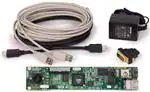


 工商网监
湘ICP备2023018690号
工商网监
湘ICP备2023018690号
